

Page 1

AN994
Application note
L638xE application guide
Introduction
STMicroelectronics’ L638xE is a versatile, high-voltage gate driver family of devices.
Developed using BCD offline technology, the L6384E, L6385E, L6386E, L6387E and
L6388E devices can operate with high voltage rails up to 600 V. The gate drivers provide all
the functions and current capability necessary for high- and low-side power MOSFETs and
IGBTs.
The devices can be used in all types of applications where high-voltage shifted control is
necessary; they have a relatively high driver current capability and are provided with an
internal patented circuitry that replaces the external bootstrap diode. This feature is
achieved by means of a high voltage DMOS, synchronously driven with the low-side gate
driver.
February 2009 Rev 7 1/25
www.st.com
Page 2

Contents AN994
Contents
1 L6384E . . . . . . . . . . . . . . . . . . . . . . . . . . . . . . . . . . . . . . . . . . . . . . . . . . . . 4
2 L6385E . . . . . . . . . . . . . . . . . . . . . . . . . . . . . . . . . . . . . . . . . . . . . . . . . . . . 7
3 L6386E . . . . . . . . . . . . . . . . . . . . . . . . . . . . . . . . . . . . . . . . . . . . . . . . . . . 10
4 L6387E . . . . . . . . . . . . . . . . . . . . . . . . . . . . . . . . . . . . . . . . . . . . . . . . . . . 13
5 L6388E . . . . . . . . . . . . . . . . . . . . . . . . . . . . . . . . . . . . . . . . . . . . . . . . . . . 15
6 Bootstrap driver . . . . . . . . . . . . . . . . . . . . . . . . . . . . . . . . . . . . . . . . . . . 17
6.1 C
selection and charging . . . . . . . . . . . . . . . . . . . . . . . . . . . . . . . . . 17
BOOT
7 Application examples . . . . . . . . . . . . . . . . . . . . . . . . . . . . . . . . . . . . . . . 20
8 Revision history . . . . . . . . . . . . . . . . . . . . . . . . . . . . . . . . . . . . . . . . . . . 24
2/25
Page 3

AN994 List of figures
List of figures
Figure 1. L6384E internal block diagram . . . . . . . . . . . . . . . . . . . . . . . . . . . . . . . . . . . . . . . . . . . . . . . 5
Figure 2. L6384E - schematic diagram of the evaluation circuit . . . . . . . . . . . . . . . . . . . . . . . . . . . . . 5
Figure 3. L6384E - PCB and component layout of the evaluation circuit. . . . . . . . . . . . . . . . . . . . . . . 6
Figure 4. L6385E - internal block diagram . . . . . . . . . . . . . . . . . . . . . . . . . . . . . . . . . . . . . . . . . . . . . . 8
Figure 5. L6385E - schematic diagram of the evaluation circuit . . . . . . . . . . . . . . . . . . . . . . . . . . . . . 8
Figure 6. L6385E - PCB and component layout of the evaluation circuit. . . . . . . . . . . . . . . . . . . . . . . 9
Figure 7. L6386E - internal block diagram . . . . . . . . . . . . . . . . . . . . . . . . . . . . . . . . . . . . . . . . . . . . . 11
Figure 8. L6386E - schematic diagram of the evaluation circuit . . . . . . . . . . . . . . . . . . . . . . . . . . . . 11
Figure 9. L6386E - PCB and component layout of the evaluation circuit. . . . . . . . . . . . . . . . . . . . . . 12
Figure 10. L6387E - internal block diagram . . . . . . . . . . . . . . . . . . . . . . . . . . . . . . . . . . . . . . . . . . . . . 14
Figure 11. L6388E internal block diagram . . . . . . . . . . . . . . . . . . . . . . . . . . . . . . . . . . . . . . . . . . . . . . 16
Figure 12. External bootstrap diode: principle schematic . . . . . . . . . . . . . . . . . . . . . . . . . . . . . . . . . . 18
Figure 13. Internal bootstrap diode: principle schematic . . . . . . . . . . . . . . . . . . . . . . . . . . . . . . . . . . . 18
Figure 14. External charge pump. . . . . . . . . . . . . . . . . . . . . . . . . . . . . . . . . . . . . . . . . . . . . . . . . . . . . 19
Figure 15. L6384E µC 3-phase motor control . . . . . . . . . . . . . . . . . . . . . . . . . . . . . . . . . . . . . . . . . . . 20
Figure 16. L6384E dimmable lamp ballast. . . . . . . . . . . . . . . . . . . . . . . . . . . . . . . . . . . . . . . . . . . . . . 21
Figure 17. L6384E half bridge converter . . . . . . . . . . . . . . . . . . . . . . . . . . . . . . . . . . . . . . . . . . . . . . . 21
Figure 18. L6385E horizontal deflection stage. . . . . . . . . . . . . . . . . . . . . . . . . . . . . . . . . . . . . . . . . . . 22
Figure 19. L6385E 2-switch forward converter . . . . . . . . . . . . . . . . . . . . . . . . . . . . . . . . . . . . . . . . . . 22
Figure 20. L6385E asymmetrical half bridge . . . . . . . . . . . . . . . . . . . . . . . . . . . . . . . . . . . . . . . . . . . . 23
Figure 21. L6386E h-bridge with cycle-by-cycle control . . . . . . . . . . . . . . . . . . . . . . . . . . . . . . . . . . . 23
3/25
Page 4
L6384E AN994
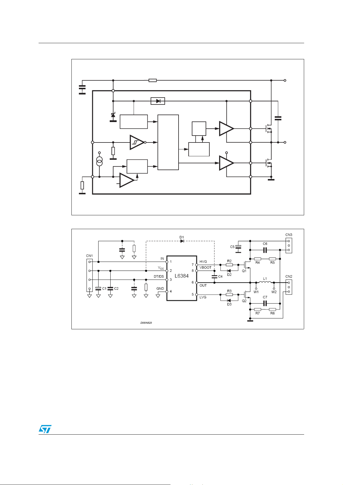
1 L6384E
The L6384E (depicted in Figure 1) is a half-bridge driver with an externally-adjustable dead
time and shut-down function. To disable the driver, the control pin (DT/SD at pin 3) must be
pulled down to below 0.5 V. The dead time can be set from 0.5 µs to 2.7 µs by placing a
resistor between pin 3 and ground. Available in both Minidip and SO-8 packages, this driver
can be used in motor controls, resonant converters and lighting applications. Figure 2 and
Figure 3 show the schematic diagram of the evaluation circuit and the layout of the test PCB.
Table 1. L6384E pin description
N. Name Typ. Function
1 IN
2 V
3 DT/SD I
4 GND Ground.
5 LVG O
6 OUT O
(1)
I Logic input. In phase with HVG and in opposition to LVG. Compatible with the VCC voltage.
CC
Supply input voltage. Includes an internal clamp (typically 15.6 V). Also has a UVLO feature
(typical threshold value V
ccth1
= 12 V, V
High impedance pin with double function. When pulled to a voltage lower than V
0.5 V) the device is shut down. A voltage higher than V
ccth2
= 10 V).
(typically
sets the dead time between the high
dt
dt
side and low side gate driver. The dead time value can be set by forcing a certain voltage level on
the pin or by connecting a resistor between pin 3 and ground. Care must be taken to avoid spikes
on pin 3 that could cause an undesired shut down of the IC. For this reason, the connection of the
components between pin 3 and ground must be as short as possible. This pin cannot be left
floating for the same reason. The pin must not be pulled through a low impedance to V
because of the drop on the current source that feeds R
.
dt
Low-side driver output. The output stage can deliver a 400 mA source and a 650 mA sink (typical
values). The circuit guarantees 0.3 V maximum on the pin (at I
= 10 mA) with V
sink
CC
lower than the turn-on threshold. This removes the need for the bleeder resistor connected
between the gate and the source of the external MOSFET normally used to hold the pin low. The
gate driver ensures low impedance in SD conditions as well.
Upper driver floating reference. Attention should be paid to the layout design of the power stage
so as to limit below-ground spikes on this pin.
CC
> 3 V and
High-side driver output. The output stage can deliver a 400 mA source and a 650 mA sink (typical
values). The circuit guarantees 0.3 V maximum between this pin and Vout (at I
> 3 V and lower than the turn-on threshold. This removes the need for the bleeder resistor
7HVG O
V
CC
connected between the gate and the source of the external MOSFET normally used to hold the
pin low. The gate driver ensures low impedance in SD conditions as well.
Bootstrap supply voltage. This is the upper driver floating supply. The bootstrap capacitor
8V
BOOT
connected between this pin and pin 6 can be fed by an internal structure named "bootstrap
driver" (a patented structure). This structure can replace the external bootstrap diode.
1. The pull-down internal resistor is typically some hundred kΩs.
4/25
= 10 mA) with
sink
Page 5
AN994 L6384E
Figure 1. L6384E internal block diagram
H.V.
V
CC
2
BOOTSTRAP DRIVER
V
8
BOOT
V
CC
HVG
DRIVER
DT/SD
UV
DETECTION
R S
1
IN
V
CC
Idt
3
Vthi
DEAD
TIME
LOGIC
LEVEL
SHIFTER
LVG
DRIVER
Figure 2. L6384E - schematic diagram of the evaluation circuit
E
C
BOOT
HVG
7
OUT
6
LVG
5
GND
4
LOAD
AM03415v1
5/25
Page 6
L6384E AN994
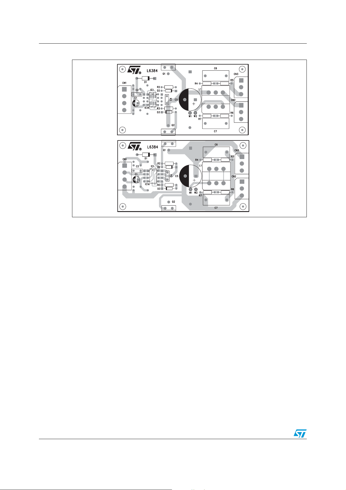
Figure 3. L6384E - PCB and component layout of the evaluation circuit
Top view
Bottom view
AM03413v1
6/25
Page 7
AN994 L6385E
2 L6385E
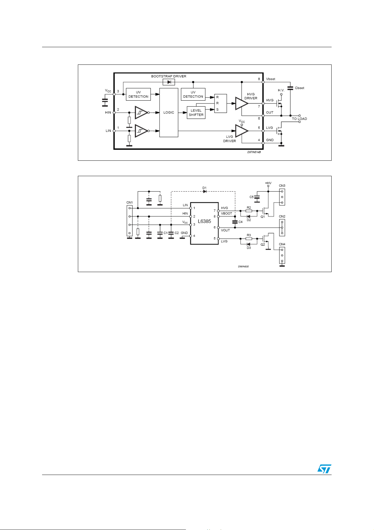
The L6385E (shown in Figure 4) is a high- and low-side configurable driver. It can control
the high- and low-side outputs (HVG and LVG) seperately, through the two related logic
inputs HIN and LIN. This device is provided with an undervoltage detection function in both
the low voltage V
packages, this driver has been specifically designed for power supplies and motion control
applications.
Figure 5 and Figure 6 show the schematic diagram of the evaluation circuit and the layout of
the relevant PCB.
Table 2. L6385E pin description
N. Name Type Function
1 LIN
2 HIN
3
4 GND Ground.
5 LVG O
6 OUT O
7 HVG O
(1)
I Low-side driver logic input. Compatible with the VCC voltage (V
(1)
I High-side driver logic input. Compatible with the VCC voltage (V
VCC Supply input voltage with UVLO (typically V
Low-side driver output. The output stage can deliver a 400 mA source and a 650 mA sink
(typical values). The circuit guarantees 0.3 V maximum on the pin (at Isink = 10 mA) with
V
CC
resistor connected between the gate and the source of the external MOSFET normally
used to hold the pin low. The gate driver ensures low impedance in SD conditions as well.
High-side driver floating reference. Attention should be paid to the layout design of the
power stage so as to limit below-ground spikes on this pin.
High-side driver output. The output stage can deliver a 400 mA source and a 650 mA sink
(typical values). The circuit guarantees 0.3 V maximum between this pin and Vout (at Isink
= 10 mA) with V
the bleeder resistor connected between the gate and the source of the external MOSFET
normally used to hold the pin low.
supply and high-voltage bootstrapped supply. Delivered in 8-pin
CC
ccth1
= 9.6 V, V
ccth2
= 1.5 V, V
il Max
= 1.5 V, V
il Max
= 8.3 V).
ih Min
ih Min
= 3.6 V)
= 3.6 V)
> 3 V and lower than the turn-on threshold. This removes the need for the bleeder
> 3 V and lower than the turn-on threshold. This removes the need for
CC
Bootstrap supply voltage. This is the floating supply of the high-side driver. Includes a
8 V
BOOT
UVLO function (typically, V
between this pin and pin 6 can be fed by an internal structure named "bootstrap driver" (a
BSth1
patented structure). This structure can replace the external bootstrap diode.
1. The pull-down internal resistor is typically some hundred kΩs.
= 9.5 V, V
= 8.2 V). The bootstrap capacitor connected
BSth2
7/25
Page 8
L6385E AN994
Figure 4. L6385E - internal block diagram
Figure 5. L6385E - schematic diagram of the evaluation circuit
E
8/25
Page 9

AN994 L6385E
Figure 6. L6385E - PCB and component layout of the evaluation circuit
Top view
Bottom view
AM03414v1
9/25
Page 10
L6386E AN994
3 L6386E
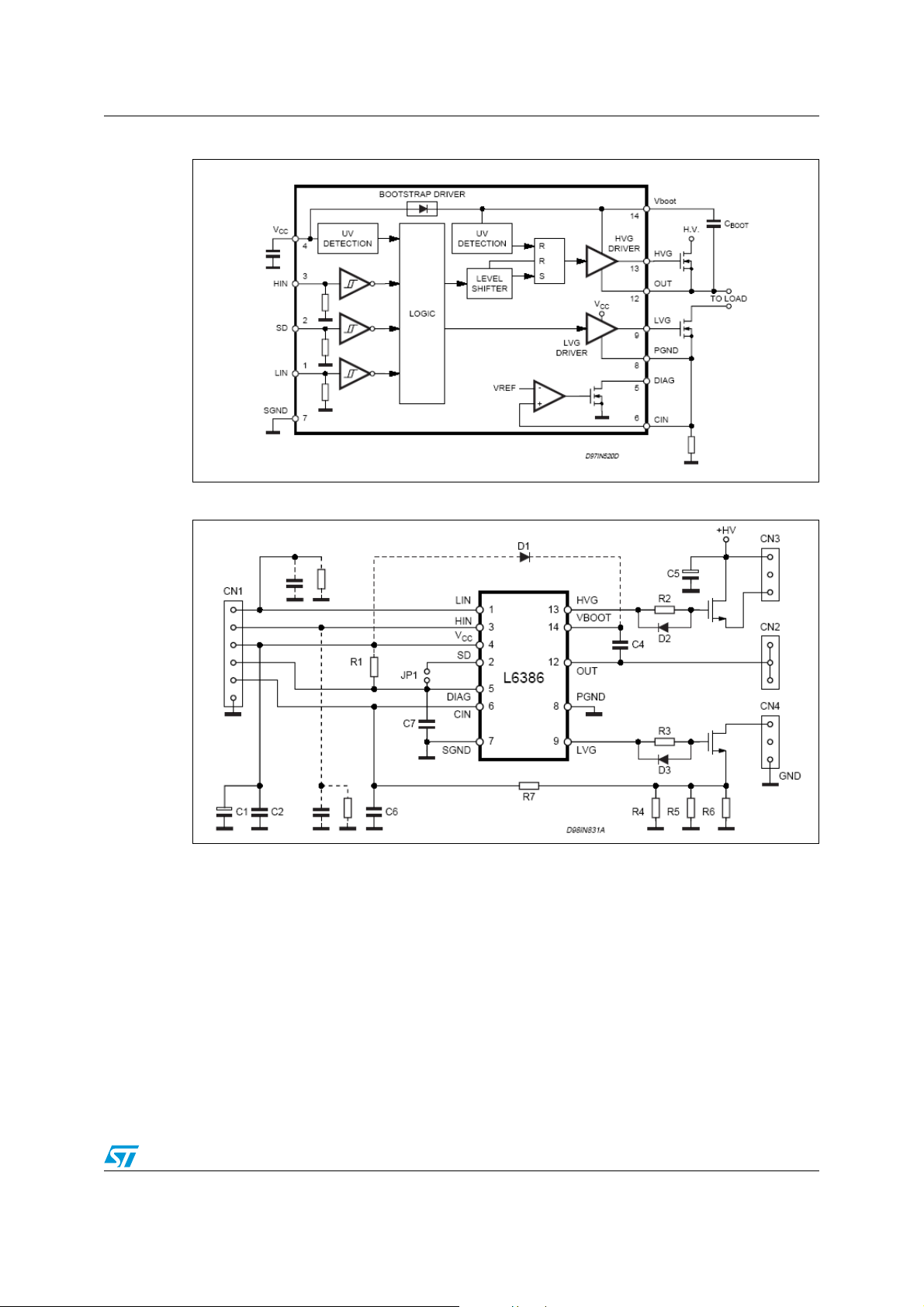
The L6386E (shown in Figure 7) is a configurable driver based on the structure of the
L6385E, with added functions. This device is available in DIP14 or SO-14 packages.
The added shutdown function (active low) and the current sense comparator (0.5-V
threshold) with diagnostic output, make this device particularly suitable for motion control
applications with cycle-by-cycle current feedback. The DIAG and CIN pins can be used to
stop the device (by acting on the SD pin). Figure 8 and Figure 9 show the schematic
diagram of the evaluation circuit and the layout of the relevant PCB.
Table 3. L6386E pin description
N. Name Type Function
1 LIN
2 SD
3 HIN
4
5 DIAG O Diagnostic output: open drain.
6 CIN I Comparator input.
(1)
I Lower driver logic input. Compatible with the V
(1)
(1)
VCC Supply input voltage with UVLO (typically V
Shut-down logic input. Compatible with the V
I
suggested resistor value is 5 to 10 kΩ. (V
il Max
I Low-side driver logic input. Compatible with the VCC voltage.
voltage (V
CC
voltage. If it needs to be pulled up, the
CC
= 1.5 V, V
ccth1
= 12 V, V
ih Min
ccth2
il Max
= 3.6 V).
= 10 V).
= 1.5 V, V
ih Min
= 3.6 V).
7 SGND Ground reference for logic signals.
8 PGND Power ground reference for the low voltage gate driver.
Low-side driver output. The output stage can deliver a 400 mA source and a 650 mA sink
(typical values). The circuit guarantees 0.3 V maximum on the pin (at I
V
9 LVG O
> 3 V and lower than the turn-on threshold. This removes the need for the bleeder
CC
resistor connected between the gate and the source of the external MOSFET normally
used to hold the pin low. The gate driver ensures low impedance in SD conditions as well.
10, 11 N.C. Not connected.
12 OUT O
High-side floating driver. Attention should be paid to the layout design of the power stage
so as to limit below-ground spikes on this pin.
High-side driver output. The output stage can deliver a 400 mA source and a 650 mA sink
(typical values). The circuit guarantees 0.3 V maximum between this pin and Vout (at
13 HVG O
= 10 mA) with V
I
sink
for the bleeder resistor connected between the gate and the source of the external
> 3 V and lower than the turn-on threshold. This removes the need
CC
MOSFET normally used to hold the pin low. The gate driver ensures low impedance in SD
conditions as well.
Bootstrapped supply voltage. This is the floating supply of the high-side driver. Includes a
14 V
BOOT
UVLO function (typically, V
between this pin and pin 12 can be fed by an internal structure named "bootstrap driver" (a
Bth1
= 11.9V, V
= 9.9 V). The bootstrap capacitor connected
Bth2
patented structure). This structure can replace the external bootstrap diode.
1. The pull-down internal resistor is typically some hundred kΩs.
= 10 mA) with
sink
10/25
Page 11
AN994 L6386E
Figure 7. L6386E - internal block diagram
Figure 8. L6386E - schematic diagram of the evaluation circuit
E
11/25
Page 12
L6386E AN994
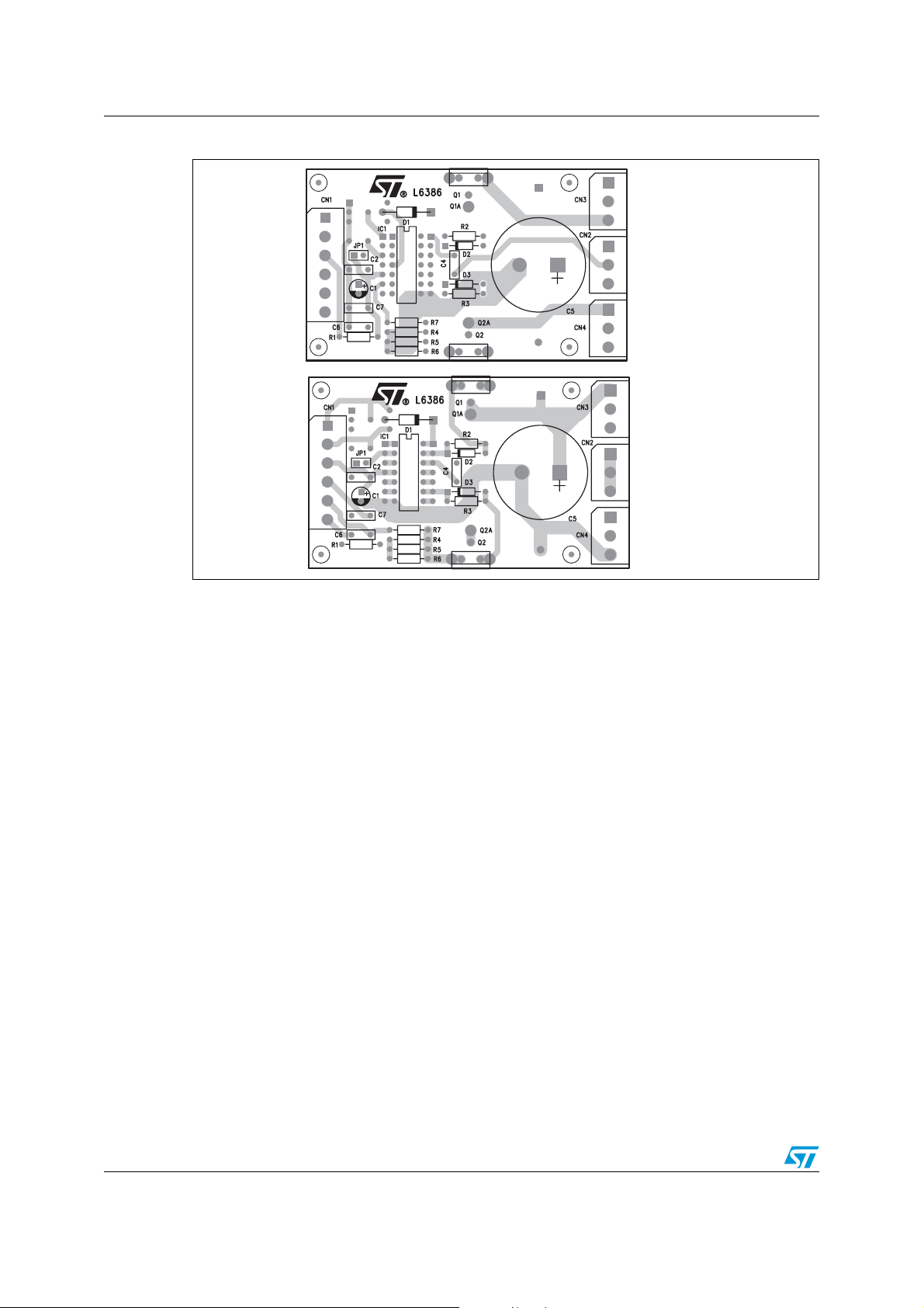
Figure 9. L6386E - PCB and component layout of the evaluation circuit
Top view
Bottom view
AM03417v1
12/25
Page 13

AN994 L6387E
4 L6387E
The L6387E (shown in Figure 10) is based on the structure of the L6385E. It has two
separate inputs and also includes an interlocking function to avoid both power switches from
being unintentionally switched on at the same time (see Ta bl e 5 ).
The V
turn-on and turn-off thresholds have been lowered to 6 and 5.5 V respectively
CC
(typical). There is no UVLO on the upper driving section.
The L6387E can be evaluated using the L6385E board.
Table 4. L6387E pin description
N. Name Type Function
1 LIN
2 HIN
3
4 GND Ground.
5 LVG O
6 OUT O
7 HVG O
(1)
I Low-side driver logic input. Compatible with VCC voltage (V
(1)
I High-side driver logic input. Compatible with VCC voltage (V
V
Supply input voltage (with very low UVLO: V
CC
ccth1
Low-side driver output. The output stage can deliver a 400 mA source and a 650 mA sink
(typical values). The circuit guarantees 0.3 V maximum on the pin (at I
V
> 3 V and lower than the turn-on threshold. This removes the need for the bleeder
CC
resistor connected between the gate and the source of the external MOSFET normally
used to hold the pin low.
High-side driver floating reference. Attention should be paid to the layout design of the
power stage so as to limit below-ground spikes on this pin.
High-side driver output. The output stage can deliver a 400 mA source and a 650 mA sink
(typical values). The circuit guarantees 0.3 V maximum between this pin and Vout (at
= 10 mA) with V
I
sink
> 3 V and lower than the turn-on threshold. This removes the need
CC
for the bleeder resistor connected between the gate and the source of the external
MOSFET normally used to hold the pin low.
= 6 V and V
il Max
il Max
ccth2
= 1.5 V, V
= 1.5 V, V
= 5.5 V)
sink
= 3.6 V).
ih Min
= 3.6 V).
ih Min
= 10 mA) with
Bootstrap supply voltage. This is the floating supply of the high-side driver. The bootstrap
8 V
BOOT
capacitor connected between this pin and pin 6 can be fed by an internal structure named
"bootstrap driver" (a patented structure). This structure can replace the external bootstrap
diode.
1. The pull-down internal resistor is typically some hundred kΩs.
13/25
Page 14

L6387E AN994
Figure 10. L6387E - internal block diagram
Table 5. Truth table
INPUT HIN 0 0 1 1
LIN 0 1 0 1
OUTPUT HVG 0 0 1 0
LVG 0 1 0 0
14/25
Page 15

AN994 L6388E
5 L6388E
The L6388E (see Figure 11) is based on the structure of the L6385E. It has two separate
inputs that are 3.3-V compatible, a fixed dead time of approximately 320 ns and an
interlocking function to avoid both power switches from being unintentionally switched on at
the same time (seeTa b le 5 ).
The UVLO thresholds of V
CC
and V
are the same as for the L6385E.
BOOT
The L6388E can be evaluated using the L6385E board.
Table 6. L6388E pin description
N. Name Type Function
1 LIN
2 HIN
3 V
4 GND Ground
5 LVG O
6 VOUT O
7HVG O
(1)
I Low-side driver logic input. Compatible with the VCC voltage (V
(1)
I High-side driver logic input. Compatible with the VCC voltage (V
CC
Supply input voltage with UVLO (typical V
= 9.6 V and typical V
ccth1
Low-side driver output. The output stage can deliver a 400 mA source and a 650 mA sink
(typical values). The circuit guarantees 0.3 V maximum on the pin (at I
3 V and lower than the turn-on threshold. This removes the need for the bleeder resistor
connected between the gate and the source of the external MOSFET normally used to hold the
pin low.
High-side driver floating reference. Attention should be paid to the layout design of the power
stage so as to limit below-ground spikes on this pin.
High-side driver output. The output stage can deliver a 400 mA source and a 650 mA sink
(typical values). The circuit guarantees 0.3 V maximum between this pin and V
mA) with V
>3 V and lower than the turn-on threshold. This removes the need for the bleeder
CC
resistor connected between the gate and the source of the external MOSFET normally used to
hold the pin low.
il Max
il Max
= 1.1 V, V
= 1.1 V, V
= 8.3 V).
ccth2
= 10 mA) with V
sink
ih Min
ih Min
out
= 1.8 V).
= 1.8 V).
(at I
sink
CC
= 10
>
Bootstrap supply voltage. This is the high-side driver floating supply (with UVLO: typical V
8V
BOOT
= 9.5 V, V
fed by an internal structure named "bootstrap driver" (a patented structure). This structure can
= 8.2 V). The bootstrap capacitor connected between this pin and pin 6 can be
BSth2
replace the external bootstrap diode.
1. The pull-down internal resistor is typically some hundred kΩs.
BSth1
15/25
Page 16

L6388E AN994
Figure 11. L6388E internal block diagram
16/25
Page 17

AN994 Bootstrap driver
6 Bootstrap driver
A bootstrap circuitry is required to supply the high voltage section. This function is normally
accomplished by a high-voltage fast recovery diode (see Figure 12). In the L638xE, a
patented integrated structure replaces the external diode. This structure is comprised of a
high-voltage DMOS—driven synchronously with the low-side driver (LVG)—with a diode in
series, as shown in Figure 13.
An internal charge pump (also shown in Figure 13) provides the DMOS driving voltage. The
diode connected in series to the DMOS has been added to avoid current flowing in the
opposite direction.
6.1 C
To choose the proper C
capacitor. This capacitor C
The ratio between the capacitors C
loss. It must be:
For example, if Q
would be 300 mV. If HVG needs to be supplied for a long time, the C
to take into account the leakage losses.
Another example: HVG’s steady state consumption is lower than 200 µA (which is the case
for L6385E, L6386E and L6388E, whereas for L6384E and L6387E it is lower than 100 µA).
Therefore, if HVG t
capacitor means a voltage drop of 1 V.
The internal bootstrap driver provides great advantages; it avoids use of the external fast
recovery diode (which usually has a high leakage current). This type of structure can only
work if V
of C
charge the capacitor.
BOOT
selection and charging
value the external MOSFET can be seen as an equivalent
BOOT
is related to the total gate charge of the MOSFET.
EXT
Q
C
EXT
and C
EXT
C
BOOT
is 30 nC and V
gate
is 5 ms, C
on
is close to GND (or lower) and while the LVG is ON. The charging time (T
OUT
is the time it takes for both conditions to be fulfilled and must be long enough to
BOOT
BOOT
is 10 V, C
gate
has to supply 1 µC to C
gate
-------------- -=
V
gate
is proportional to the cyclical voltage
BOOT
>>>C
EXT
is 3 nF. With C
EXT
. This charge on a 1-µF
EXT
= 100 nF the drop
BOOT
selection also has
BOOT
charge
)
The bootstrap driver introduces a voltage drop due to the DMOS R
(typical for L638xE
DS(on)
is 125 Ω). At low frequencies this drop is negligible, but when the frequency is increased it
must be taken into account.
The following equation is useful to compute the drop on the bootstrap DMOS.
Q
gate
-------------------
V
dropIch eargRDS on()Vdrop
Q
is the gate charge of the external power MOSFET, R
gate
bootstrap DMOS, and T
is the charging time of the bootstrap capacitor.
charge
17/25
=→⋅=
T
ch earg
R
DS on()
is the ON resistance of the
DS(on)
Page 18

Bootstrap driver AN994
For example, using a power MOSFET with a total gate charge of 30 nC, the drop on the
bootstrap DMOS is about 1 V if T
charge
is 5 µs.
In fact:
30 nC
-------------- -
V
drop
V
must be taken into consideration when the voltage drop on C
drop
5 µs
125 Ω 0.8 V≈⋅=
is calculated. If the
BOOT
drop is too high or the circuit topology does not provide for a sufficient charging time (like the
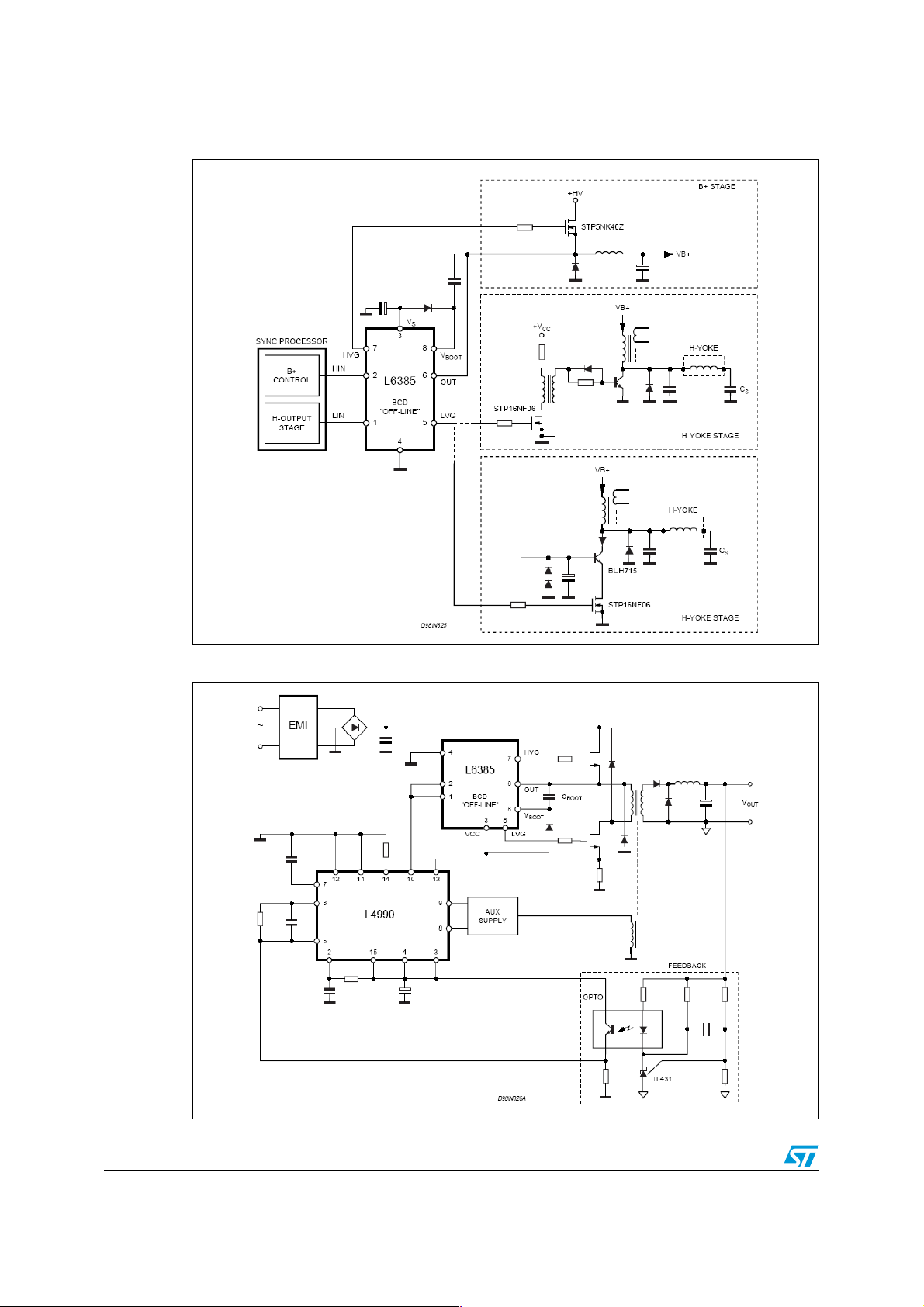
examples shown in Figure 18, Figure 19 and Figure 20), an external diode can be used.
This is the reason why the external diode D1 is dotted in Figure 2, Figure 5 and Figure 8.
When operating at very low frequencies, the high-side ON time can be very long. The
C
voltage can drop because of the steady state consumption of the HGV. To avoid
BOOT
having to use extremely large capacitors (> 1 to 2 µF), an external charge pump can be
added (see Figure 14 as an example). The diodes are signal diodes because the high
voltage drops on C1 and C2. It is mandatory that the diodes have a low parasitic
capacitance because C1 and C2 have to be greater than the diodes’ capacitance. The
oscillator has to balance the consumption of the high-voltage side and the minimum
frequency is fixed by the values of C1 and C2 (with C1 and C2 = 33 pF -> f > 250-300 kHz).
Additionally, the oscillator has to be able to sustain the dV/dt of the OUT pin.
Figure 12. External bootstrap diode: principle
schematic
Figure 13. Internal bootstrap diode: principle
schematic
18/25
Page 19

AN994 Bootstrap driver
Figure 14. External charge pump
HV
VBOOT
Cboot
200nF
LOAD
L638x
HVG
OUT
E
LVG
GND
330pF
VCC
C1
33pF
HCF4069UB
C2
33pF
Cx
19/25
Page 20

Application examples AN994
7 Application examples
This section provides several application suggestions that highlight the versatility and
flexibility of this family of high- and low-side drivers. Their simplicity and compactness make
these devices a cost-effective solution.
For further information on these ICs, refer to the following documents.
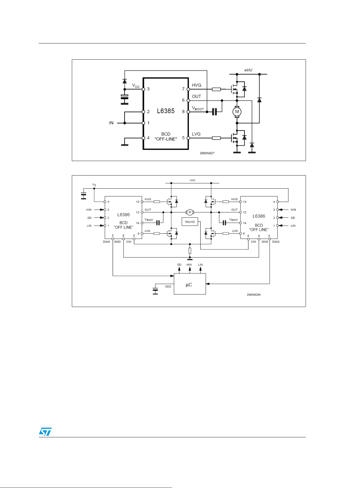
● AN1263: "Using the internal bootstrap current capability of the L638xE in driving a six
transistor inverter bridge".
● AN1299: "L638xE tricks and tips".
Figure 15. L6384E µC 3-phase motor control
E
E
E
20/25
Page 21

AN994 Application examples
Figure 16. L6384E dimmable lamp ballast
E
Figure 17. L6384E half bridge converter
E
21/25
Page 22
Application examples AN994
Figure 18. L6385E horizontal deflection stage
E
Figure 19. L6385E 2-switch forward converter
E
22/25
Page 23
AN994 Application examples
Figure 20. L6385E asymmetrical half bridge
E
Figure 21. L6386E h-bridge with cycle-by-cycle control
E
E
23/25
Page 24

Revision history AN994
8 Revision history
Table 7. Document revision history
Date Revision Changes
09-Sep-2004 6 Minor text changes
Added: Section 5: L6388E
17-Feb-2009 7
– L6384 replaced by L6384E, L6385 replaced by L6385E, L6386
replaced by L6386E, L6387 replaced by L6387E, L6388 replaced
by L6388E, L638x replaced by L638xE.
24/25
Page 25

AN994
Please Read Carefully:
Information in this document is provided solely in connection with ST products. STMicroelectronics NV and its subsidiaries (“ST”) reserve the
right to make changes, corrections, modifications or improvements, to this document, and the products and services described herein at any
time, without notice.
All ST products are sold pursuant to ST’s terms and conditions of sale.
Purchasers are solely responsible for the choice, selection and use of the ST products and services described herein, and ST assumes no
liability whatsoever relating to the choice, selection or use of the ST products and services described herein.
No license, express or implied, by estoppel or otherwise, to any intellectual property rights is granted under this document. If any part of this
document refers to any third party products or services it shall not be deemed a license grant by ST for the use of such third party products
or services, or any intellectual property contained therein or considered as a warranty covering the use in any manner whatsoever of such
third party products or services or any intellectual property contained therein.
UNLESS OTHERWISE SET FORTH IN ST’S TERMS AND CONDITIONS OF SALE ST DISCLAIMS ANY EXPRESS OR IMPLIED
WARRANTY WITH RESPECT TO THE USE AND/OR SALE OF ST PRODUCTS INCLUDING WITHOUT LIMITATION IMPLIED
WARRANTIES OF MERCHANTABILITY, FITNESS FOR A PARTICULAR PURPOSE (AND THEIR EQUIVALENTS UNDER THE LAWS
OF ANY JURISDICTION), OR INFRINGEMENT OF ANY PATENT, COPYRIGHT OR OTHER INTELLECTUAL PROPERTY RIGHT.
UNLESS EXPRESSLY APPROVED IN WRITING BY AN AUTHORIZED ST REPRESENTATIVE, ST PRODUCTS ARE NOT
RECOMMENDED, AUTHORIZED OR WARRANTED FOR USE IN MILITARY, AIR CRAFT, SPACE, LIFE SAVING, OR LIFE SUSTAINING
APPLICATIONS, NOR IN PRODUCTS OR SYSTEMS WHERE FAILURE OR MALFUNCTION MAY RESULT IN PERSONAL INJURY,
DEATH, OR SEVERE PROPERTY OR ENVIRONMENTAL DAMAGE. ST PRODUCTS WHICH ARE NOT SPECIFIED AS "AUTOMOTIVE
GRADE" MAY ONLY BE USED IN AUTOMOTIVE APPLICATIONS AT USER’S OWN RISK.
Resale of ST products with provisions different from the statements and/or technical features set forth in this document shall immediately void
any warranty granted by ST for the ST product or service described herein and shall not create or extend in any manner whatsoever, any
liability of ST.
ST and the ST logo are trademarks or registered trademarks of ST in various countries.
Information in this document supersedes and replaces all information previously supplied.
The ST logo is a registered trademark of STMicroelectronics. All other names are the property of their respective owners.
© 2009 STMicroelectronics - All rights reserved
STMicroelectronics group of companies
Australia - Belgium - Brazil - Canada - China - Czech Republic - Finland - France - Germany - Hong Kong - India - Israel - Italy - Japan -
Malaysia - Malta - Morocco - Singapore - Spain - Sweden - Switzerland - United Kingdom - United States of America
www.st.com
25/25
 Loading...