

Page 1

AN993
Application note
Electronic ballast with PFC using L6574 and L6561
Introduction
Dedicated ICs for lamp ballast applications are now replacing the old solutions based on
bipolar transistors driven by a saturable pulse transformer.
The L6574 is a high-performance ballast driver, designed using 600-V BCD offline
technology, which ensures all the features needed to properly drive and control a fluorescent
bulb. It is provided with built-in VCO start-up sequence circuitry, protections, and an
operation amplifier for implementing a closed-loop control of the lamp current.
July 2009 Doc ID 5656 Rev 10 1/27
www.st.com
Page 2

Contents AN993
Contents
1 Half bridge converter for electronic lamp ballast . . . . . . . . . . . . . . . . . . 4
1.1 Lamp requirements . . . . . . . . . . . . . . . . . . . . . . . . . . . . . . . . . . . . . . . . . . 4
2 L6574 ballast driver . . . . . . . . . . . . . . . . . . . . . . . . . . . . . . . . . . . . . . . . . . 5
3 Device block description . . . . . . . . . . . . . . . . . . . . . . . . . . . . . . . . . . . . . 8
3.1 Preheating and ignition section . . . . . . . . . . . . . . . . . . . . . . . . . . . . . . . . . 8
3.2 Control section . . . . . . . . . . . . . . . . . . . . . . . . . . . . . . . . . . . . . . . . . . . . . 12
3.3 Bootstrap section . . . . . . . . . . . . . . . . . . . . . . . . . . . . . . . . . . . . . . . . . . . 13
3.3.1 C
selection and charging . . . . . . . . . . . . . . . . . . . . . . . . . . . . . . . . . 13
boot
4 Description of the demonstration application . . . . . . . . . . . . . . . . . . . 15
4.1 Power factor section . . . . . . . . . . . . . . . . . . . . . . . . . . . . . . . . . . . . . . . . . 17
4.2 Ballast section . . . . . . . . . . . . . . . . . . . . . . . . . . . . . . . . . . . . . . . . . . . . . 17
4.3 Preheating and ignition sequence . . . . . . . . . . . . . . . . . . . . . . . . . . . . . . 18
4.4 Current feedback loop . . . . . . . . . . . . . . . . . . . . . . . . . . . . . . . . . . . . . . . 18
4.5 Start-up and supply . . . . . . . . . . . . . . . . . . . . . . . . . . . . . . . . . . . . . . . . . 19
4.6 Safety circuitry . . . . . . . . . . . . . . . . . . . . . . . . . . . . . . . . . . . . . . . . . . . . . 20
5 Design tips . . . . . . . . . . . . . . . . . . . . . . . . . . . . . . . . . . . . . . . . . . . . . . . . 21
5.1 Inductance and capacitor evaluation . . . . . . . . . . . . . . . . . . . . . . . . . . . . 21
6 Dimming the lamp . . . . . . . . . . . . . . . . . . . . . . . . . . . . . . . . . . . . . . . . . . 24
6.1 Dimming level and lamp turn-on . . . . . . . . . . . . . . . . . . . . . . . . . . . . . . . . 25
7 Revision history . . . . . . . . . . . . . . . . . . . . . . . . . . . . . . . . . . . . . . . . . . . 26
2/27 Doc ID 5656 Rev 10
Page 3

AN993 List of figures
List of figures
Figure 1. Half bridge topology . . . . . . . . . . . . . . . . . . . . . . . . . . . . . . . . . . . . . . . . . . . . . . . . . . . . . . . 4
Figure 2. Internal block diagram of the L6574 . . . . . . . . . . . . . . . . . . . . . . . . . . . . . . . . . . . . . . . . . . . 5
Figure 3. Connection of a typical application . . . . . . . . . . . . . . . . . . . . . . . . . . . . . . . . . . . . . . . . . . . . 6
Figure 4. Startup timing diagram and EN2 function . . . . . . . . . . . . . . . . . . . . . . . . . . . . . . . . . . . . . . . 8
Figure 5. Timing block . . . . . . . . . . . . . . . . . . . . . . . . . . . . . . . . . . . . . . . . . . . . . . . . . . . . . . . . . . . . . 9
Figure 6. Timing oscillator block . . . . . . . . . . . . . . . . . . . . . . . . . . . . . . . . . . . . . . . . . . . . . . . . . . . . . 9
Figure 7. Cpre voltage and frequency shifting . . . . . . . . . . . . . . . . . . . . . . . . . . . . . . . . . . . . . . . . . . 11
Figure 8. Operating frequency at Cf = 470 pF . . . . . . . . . . . . . . . . . . . . . . . . . . . . . . . . . . . . . . . . . . 11
Figure 9. Controls timing diagram . . . . . . . . . . . . . . . . . . . . . . . . . . . . . . . . . . . . . . . . . . . . . . . . . . . 12
Figure 10. Startup timing diagram and EN2 function . . . . . . . . . . . . . . . . . . . . . . . . . . . . . . . . . . . . . . 13
Figure 11. External bootstrap diode connection . . . . . . . . . . . . . . . . . . . . . . . . . . . . . . . . . . . . . . . . . 14
Figure 12. L6574 integrated bootstrap diode connection. . . . . . . . . . . . . . . . . . . . . . . . . . . . . . . . . . . 14
Figure 13. Demonstration application circuit . . . . . . . . . . . . . . . . . . . . . . . . . . . . . . . . . . . . . . . . . . . . 15
Figure 14. PCB and components layouts . . . . . . . . . . . . . . . . . . . . . . . . . . . . . . . . . . . . . . . . . . . . . . 16
Figure 15. Current feedback loop . . . . . . . . . . . . . . . . . . . . . . . . . . . . . . . . . . . . . . . . . . . . . . . . . . . . 19
Figure 16. Cpre waveform (Ch1) and amplifier output (Ch2) . . . . . . . . . . . . . . . . . . . . . . . . . . . . . . . . 19
Figure 17. Open load safety circuit . . . . . . . . . . . . . . . . . . . . . . . . . . . . . . . . . . . . . . . . . . . . . . . . . . . 20
Figure 18. Extra voltage safety circuit . . . . . . . . . . . . . . . . . . . . . . . . . . . . . . . . . . . . . . . . . . . . . . . . . 20
Figure 19. Simplified schematic of the lamp . . . . . . . . . . . . . . . . . . . . . . . . . . . . . . . . . . . . . . . . . . . . 21
Figure 20. Preheating transfer function . . . . . . . . . . . . . . . . . . . . . . . . . . . . . . . . . . . . . . . . . . . . . . . . 22
Figure 21. Operating transfer function . . . . . . . . . . . . . . . . . . . . . . . . . . . . . . . . . . . . . . . . . . . . . . . . . 23
Figure 22. Iterative process . . . . . . . . . . . . . . . . . . . . . . . . . . . . . . . . . . . . . . . . . . . . . . . . . . . . . . . . . 23
Doc ID 5656 Rev 10 3/27
Page 4
Half bridge converter for electronic lamp ballast AN993
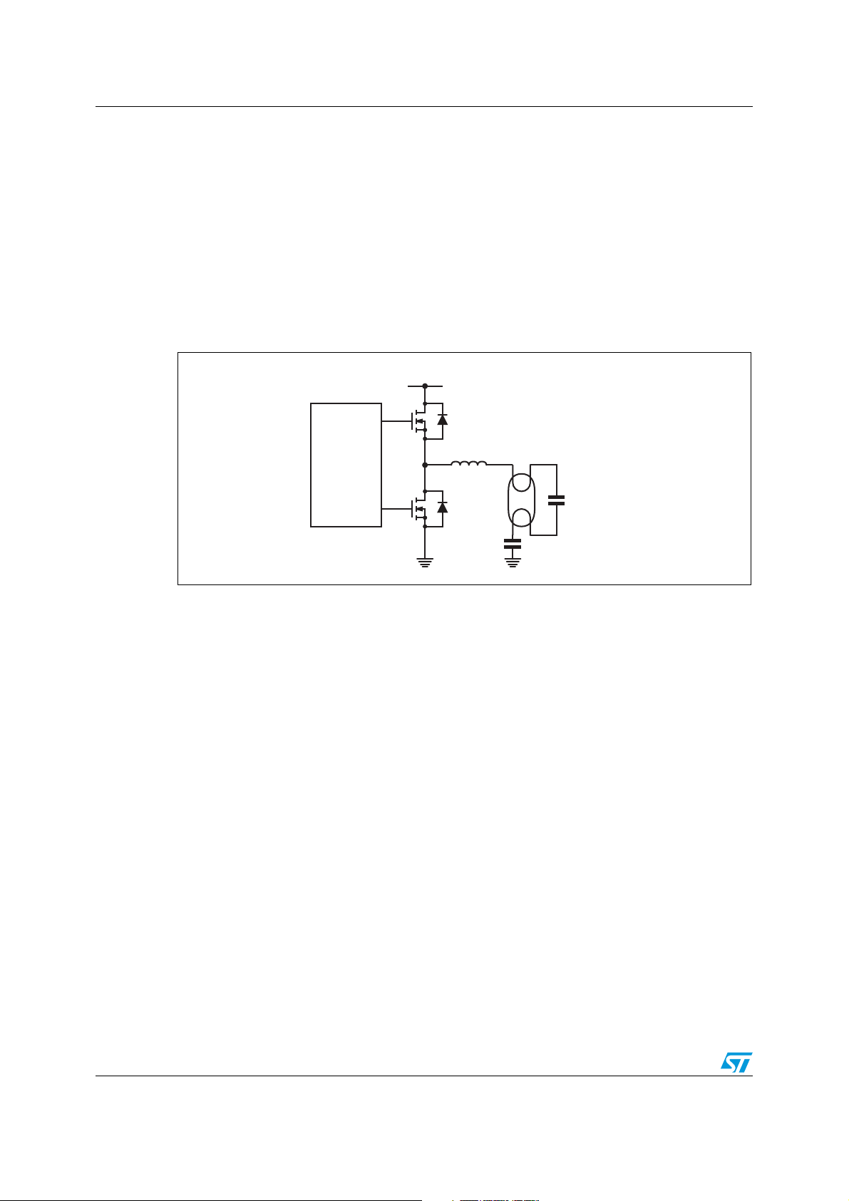
1 Half bridge converter for electronic lamp ballast
Voltage-fed, series-resonant half-bridge inverters are currently used for fluorescent lamps
(Figure 1). This topology facilitates operation in zero voltage switching (ZVS) resonant
mode, dramatically reducing the transistor switching losses and the electromagnetic
interference.
To design a cost-effective, compact and smart electronic lamp ballast, a dedicated IC could
be used to drive directly the power MOSFETs of the half bridge. Such controllers require a
high voltage capability for the high-side floating transistor driver.
Figure 1. Half bridge topology
HV
DRIVER
1.1 Lamp requirements
To prolong lamp life and to ensure efficient ignition of the lamp, the cathodes must be
preheated. In fact, the preheating of the filaments allows an easy strike of the lamp, reducing
the ignition voltage. During the preheating time, the lamp is characterized by a high
impedance and the current flows only in the filaments. The resistance value of the filaments
strictly depends on the type of lamp. Typically, these filaments present an initial low value (a
few Ohms) that will increase by four to five times during the preheating phase.
After the preheating phase, the lamp must be ignited by increasing the voltage across it. The
ignition voltage value also depends on the type of lamp, and it increases with the aging of
the lamp. For a typical TL 58 W, the ignition voltage value is not much less than 1000 V.
When a simple inverter with a constant switching frequency is used, external circuitry is also
necessary (for example, a PTC or discrete timer). However, with ST’s L6574 smart
controller, both the preheating and ignition functions are achieved by using simple resistors
and a capacitor, which set all the start-up procedures.
L
RES
C
RES
AM01309v1
4/27 Doc ID 5656 Rev 10
Page 5
AN993 L6574 ballast driver
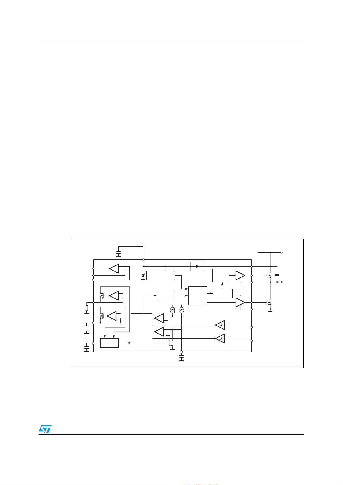
2 L6574 ballast driver
The L6574, whose internal block diagram is shown in Figure 2, is an IC intended to drive two
power MOSFETs or IGBTs in half-bridge topology, ensuring all the features needed to
properly drive and control a fluorescent bulb. Moreover, by varying the switching frequency,
it is possible to modulate the current in the lamp and as a consequence, the output power as
well. The device is available in DIP16 and SO16N packages.
The L6574 has the following distinctive features.
● High voltage rail up to 600 V
● dV/dt immunity ± 50 V/ns in full temperature range
● Driver current capability (250 mA source and 450 mA sink)
● Switching times 80/40 ns rise fall with 1 nF load
● CMOS shutdown input
● Under-voltage lock-out
● Preheat and frequency shifting timing
● Sense operational amplifier for closed-loop control or protection features
● High-accuracy current-controlled oscillator
● Integrated bootstrap diode
● Clamping on VS
● SO16, DIP16 package.
Figure 2. Internal block diagram of the L6574
H.V.Bus
Cboot
LOAD
OPOUT
OPIN-
OPIN+
Rign
Rpre
Cf
VS
OP AMP
5
6
7
4
2
3
Imin
Imax
VCO
+
-
REF
V
V
REF
12
CONTROL
LOGIC
UV
DETECTION
DEAD
TIME
+
-
+
-
Ifs
Vthpre
Ipre
BOOTSTRAP
1
Cpre
DRIVER
DRIVING
LOGIC
HVG
DRIVER
LEVEL
SHIFTER
DRIVER
+
-
+
-
LVG
V
VTHE
THE
16
Vboot
HVG
15
14
OUT
V
S
11
LVG
10
GND
8
EN1
9
EN2
AM01310v1
Doc ID 5656 Rev 10 5/27
Page 6
L6574 ballast driver AN993
Figure 3. Connection of a typical application
+
HVBus
CSupply
Ref.
Table 1. Description of device pins
Number Name Function
Preheat timing capacitor. The capacitor C
shift time, according to the relations: t
1.5 s/ ∝F, KFS= 0.15s/∝F). This feature is obtained by charging C
1 C
pre
is charged up to 3.5 V (preheat timing comparator threshold). During tSH, the current
currents. During t
depends on the value of R
way t
Figure 5).
Maximum oscillation frequency setting. The resistance connected between this pin
2 R
pre
and ground sets the f
the end of the start-up procedure, the effect current drown from R
voltage at this pin is fixed at V
3 CF
4 R
ign
5 OPout
Oscillator frequency setting. The capacitor C
and f
Minimum oscillation frequency setting. The resistance connected between this pin
and ground sets the f
Out of the operational amplifier. To implement a feedback control loop this pin can be
connected to the R
6 OPin- Inverting input of the operational amplifier.
7 OPin+ Non-inverting Input of the operational amplifier.
D1
D2
R1
Rpre.
C1
C2
R3
pre
is always set at 0.1t
SH
. In normal operation this pin shows a triangular wave.
ING
CSnub
D3
12
2
7
6
L6574
5
410
Rign.
3
Cf
R2
CBoot
15
16
14
11
8
9
1
Cpre
C3
R4
pre
= K
pre
Qh
Rgh
Ql
Rgl
R5
D4
Rcs
sets the preheating and the frequency
· C
pre
and tSH= KFS· C
pre
, this current is independent of the external components, so C
(that is, on the difference between f
pre
. In steady state the voltage at pin 1 is 5 V (see
pre
value, fixing the difference between f
pre
=2 V.
REF
, along with to R
F
value. The voltage at this pin is fixed at V
ign
pin by means of appropriate circuitry.
ign
L_ballast
R6
R7
LAMP
pre
Cb
Cres
R9
C4
R8
pre
with two different
pre
and f
pre
and f
ign(fpre
is over. The
pre
and R
pre
=2 V.
REF
(typ. K
ign
, sets f
ign
AM01311v1
=
pre
). In this
> f
). At
ign
pre
pre
6/27 Doc ID 5656 Rev 10
Page 7

AN993 L6574 ballast driver
Table 1. Description of device pins (continued)
Number Name Function
Enable 1. This pin (active high), forces the device into a latched shutdown state (like
in undervoltage conditions). There are two ways of resuming normal operation: the
8 EN1
9 EN2
10 GND Ground.
11 LVG
12 VS Supply voltage. This pin is connected to the supply filter capacitor (15.6 V typical).
13 N.C.
14 OUT
first is by reducing the supply voltage below the undervoltage threshold and then
increasing it again until the valid supply is recognized; the second is by activating the
EN2 input (see Figure 9). The Enable 1 is specifically designed for strong faults (for
example, in case of lamp disconnection).
Enable 2. EN2 input (active high) restarts the start-up procedure (preheating and
ignition sequence). This feature is useful if the lamp does not turn on after the first
ignition sequence (see Figure 10).
Low-side driver output. This pin must be connected to the low-side power MOSFET
gate of the half bridge. A resistor connected between this pin and the power
MOSFET gate can be used to reduce the peak current.
Not connected. This pin sets a distance between the pins related to the high-voltage
side and those related to the low-voltage side.
High-side driver floating reference. This pin must be connected close to the source of
the high-side power MOSFET or IGBT.
High-side driver output. This pin must be connected to the high-side power MOSFET
15 HVG
gate of the half bridge. A resistor connected between this pin and the power
MOSFET gate can be used to reduce the peak current.
Bootstrapped supply voltage. The bootstrap capacitor must be connected between
16 VBOOT
this pin and OUT. A patented integrated circuit replaces the external bootstrap diode
by means of a high-voltage DMOS, synchronously driven with the low-side power
MOSFET.
Doc ID 5656 Rev 10 7/27
Page 8
Device block description AN993
3 Device block description
The preheating control section and the bootstrap section are tightly linked to the
application’s design. This chapter describes their workings and usage.
3.1 Preheating and ignition section
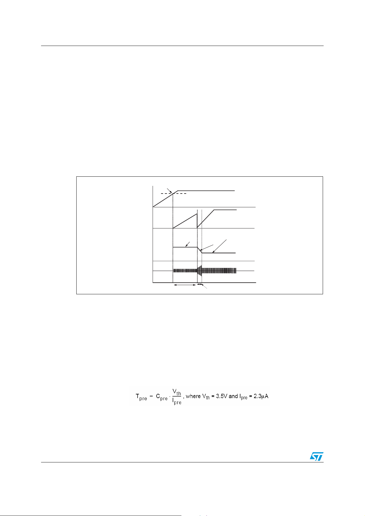
The L6574’s turn-on sequence is divided into three phases: the preheating phase, the
ignition phase and the normal operation phase (Figure 4). The preheating phase is
characterized by the highest oscillation frequency (f
phase, the frequency shifts from f
period T
Figure 4. Startup timing diagram and EN2 function
sh
.
Power-O.K.
VSupply
max
to f
(which is the normal operating frequency) in a
min
) for a period T
max
. During the ignition
pre
V(Cpre)
Osc.
freq.
IL
T
K= C
●
pre
T
●
IGN
⋅
0.1= T
⋅
pre
pre
preheating
f
MAX
T
PRE
steady state operation
ignition
fMIN
Time
All the above-mentioned parameters are set by carefully selecting a few external
components. T
During the preheating phase (T
current I
pre,
The voltage across C
and Tsh are set by means of the capacitor C
pre
the capacitor C
pre)
is charged by means of a constant
pre
that is connected to pin 1.
pre
which is generated internally and does not depend on any external components.
increases linearly up to the "preheating threshold" at which the
pre
preheating phase terminates.
Equation 1
AM01312v1
8/27 Doc ID 5656 Rev 10
Page 9
AN993 Device block description
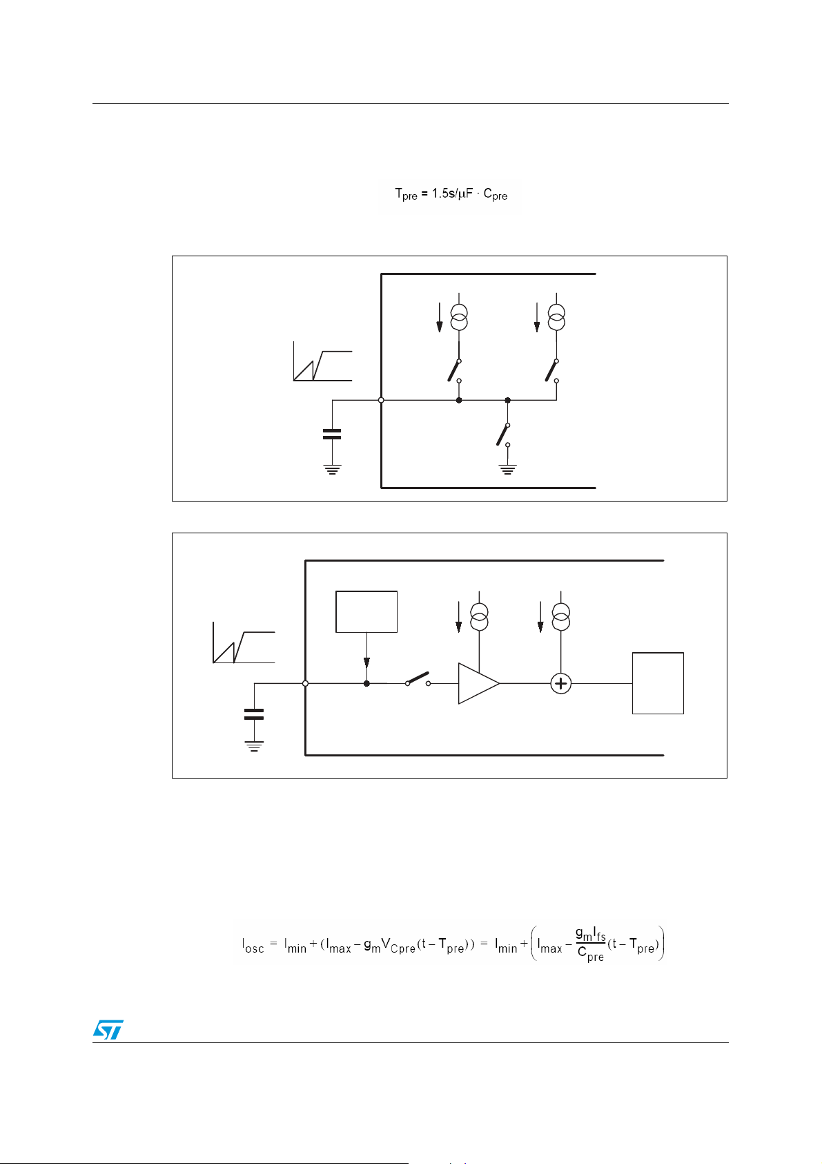
That is to say:
Equation 2
Figure 5. Timing block
Ifs Ipre
Cpre
Figure 6. Timing oscillator block
TIMING
DISCHARGE
IminImax
Iosc
AM01313v1
CSOmg
Cpre
AM01314v1
After the preheating time, the capacitor C
by the current I
, generating a second voltage ramp which feeds a transconductance
fs
is first quickly discharged and then recharged
pre
amplifier, as shown in Figure 6 (the switch is closed). Thus, this voltage signal is converted
into a growing current which is subtracted from I
f
to f
max
. The current that drives the oscillator to set the frequency during this shifting is
min
to produce the frequency shifting from
max
equal to:
Equation 3
Doc ID 5656 Rev 10 9/27
Page 10

Device block description AN993
Where:
Equation 4
R
and R
ign
At the end of the preheating time (t = T
are the resistors connected to pin 4 and pin 2.
pre
), the L6574 oscillates at f
pre
max
, set by:
Equation 5
This means that the preheating frequency depends on both R
At the end of the frequency shifting (t = T
+ Tsh), the second term of Equation 3
pre
decreases to zero and the switching frequency is set only by I
Equation 6
Since the second term of Equation 3 is equal to zero, we have:
Equation 7
Note that there is no fixed voltage threshold across C
(that is, the end of the frequency shifting): T
depends on C
sh
in which the ignition phase finishes
pre
pre
(Equation 7). This fact is also verified in Figure 7. By making T
current has been designed to be a fraction of I
, therefore:
max
Equation 8
and R
pre
(that is, R
min
, I
max
independent of I
sh
.
ign
, gm, and Ifs
ign
).
, the Ifs
max
In this way, the frequency shifting time depends only on the capacitor C
of the kfs constant (frequency shift timing constant) is 0.15 s/µF, that is:
Equation 9
So when choosing C
The frequencies f
capacitor C
R
, then with R
ign
(oscillator frequency setting -> capacitor at pin 3). f
f
pre
and f
min
the Δf = f
pre
, both T
max
and Tsh are set.
pre
depend on the resistors R
- f
max
min
Simplified equations can be used.
10/27 Doc ID 5656 Rev 10
is set.
pre
and R
min
. The typical value
pre
, but also on the
ign
is set by choosing Cf and
Page 11

AN993 Device block description
Equation 10
Equation 11
These equations fit well with the measured values, especially in the frequency range of 30 to
100 kHz. Figure 8 shows a comparison between the measured and computed data of f
(at C
= 470 pF).
f
Figure 7. C
V(Cpre)
freq
voltage and frequency
pre
shifting
preheating
ignition
time
Figure 8. Operating frequency at Cf =
470 pF
120
100
80
(kHz)
min
f
60
40
measured values
computed values
min
20
time
AM01315v1
40 60 80 100 120
R
(kΩ)
ign
AM01316v1
To summarize:
Table 2. Parameter dependencies
Parameter Set by choosing...
T
C
pre
Tsh C
Δf = f
If R
is not connected at pin 2, there is no Δf, so f
pre
Furthermore, there is no I
charged only once by I
When C
is discharged, no Ifs current is present to recharge it. If R
pre
the preheating and ignition phases, pin 1(C
few µA (1/6 IR
phase.
pre
). If R
- f
max
f
min
pre
R
max
R
and f
, that is to say there is no Ifs current. In this case, C
max
max
= 2.3 µA up to 3.5 V (Figure 7 shows the first voltage rise only).
pre
) is at 4.8 to 5 V with a current capability of a
is not connected, C
pre
is at GND level in the normal operation
pre
min
pre
pre
pre
and Cf
ign
have the same value.
is
pre
is connected after
pre
Doc ID 5656 Rev 10 11/27
Page 12

Device block description AN993
3.2 Control section
The L6574 has two control functions, EN1 and EN2. Both functions are active high. To fully
understand how these functions work, refer to Figure 9 and Figure 10.
● EN1 (latched enable) is dedicated to stopping all device functions and is usually
activated when a strong fault is detected (for example, when the lamp is disconnected).
This status can be cancelled in two different ways: either by reducing the supply voltage
below its minimum threshold, or by activating the second control pin EN2 (EN2
overrides EN1). When the device restarts, the start-up sequence is reactivated.
● EN2 (repeating startup) is dedicated to restarting the preheating and ignition
procedure; it is normally activated when the application fails to ignite the lamp. When
EN2 is activated the starting procedure restarts. The L6574 operates to the maximum
frequency all the while that EN2 remains active.
Figure 9. Controls timing diagram
VSupply
LVG
HVG
EN1
EN2
Latched enable
Forced restart
Time
AM01318v1
12/27 Doc ID 5656 Rev 10
Page 13

AN993 Device block description
Figure 10. Startup timing diagram and EN2 function
VSupply
V(Cpre)
EN2
IL
f
MAX
3.3 Bootstrap section
Bootstrap circuitry is needed to supply the high-voltage section. This function is normally
accomplished by a high-voltage fast-recovery diode (Figure 11). In the L6574, a patented
integrated structure replaces the external diode. It is realized by means of a high-voltage
DMOS, driven synchronously with the low-side driver (LVG), with a diode connected in
series, as shown in Figure 12. An internal charge pump (Figure 12) provides the DMOS
driving voltage.
The diode connected in series to the DMOS has been added to avoid it being unintentionally
turned on.
preheating
T
PRE
ignition
f
MIN
IGN(TSH
T
preheating
Foult-ignition
)
ignition
Time
AM01317v1
3.3.1 C
selection and charging
boot
To choose the proper C
This capacitor C
is related to the total gate charge of the MOS.
ext
value, the external MOS can be seen as an equivalent capacitor.
boot
Equation 12
The ratio between the capacitors C
has to be:
Equation 13
For example, if Q
is 30 nC and V
gate
would be 300 mV.
Doc ID 5656 Rev 10 13/27
ext
gate
and C
is proportional to the cyclical voltage loss. It
boot
is 10 V, C
is 3 nF. With C
ext
= 100 nF, the drop
boot
Page 14

Device block description AN993
If the HVG needs to be supplied for a long period of time, the C
selection also has to take
boot
into account the leakage losses.
The internal bootstrap driver has great advantages: the external fast-recovery diode can be
avoided (it usually has great leakage current). This structure can only work if V
GND (or lower) and if in the meanwhile the LVG is on. The charging time (T
C
is the time in which both conditions are fulfilled and it has to be long enough to charge
boot
out
charge
is close to
) of the
the capacitor.
The bootstrap driver introduces a voltage drop due to the DMOS R
(typical value at
DS(on)
25°C is 150 Ω). At low frequencies, this drop can be neglected, but must be taken into
account when the frequency is increased.
The following equation is useful to compute the drop on the bootstrap DMOS.
Equation 14
Q
gate
V
dropIch eargRDS on()Vdrop
where Q
is the gate charge of the external power MOSFET, R
gate
of the bootstrap DMOS, and T
is the charging time of the bootstrap capacitor.
charge
-----------------------
=→=
T
ch earg
R
DS on()
DS(on)
is the on resistance
For example: using a power MOSFET with a total gate charge of 30 nC, the drop on the
bootstrap DMOS is about 1 V if the T
is 5 µs. In fact:
charge
Equation 15
V
has to be taken into account when the voltage drop on C
drop
is calculated: if this drop
boot
is too high or if the charging time is insufficient, an external diode can be used.
Figure 11. External bootstrap diode
V
S
connection
D
BOOT
HVG
LVG
V
V
BOOT
OUT
H.V.
C
BOOT
TO LOAD
AM01319v1
Figure 12. L6574 integrated bootstrap
diode connection
V
V
BOOT
OUT
H.V.
C
BOOT
TO LOAD
EX_D99IN1056
AM01320v1
V
S
HVG
LVG
14/27 Doc ID 5656 Rev 10
Page 15

AN993 Description of the demonstration application
4 Description of the demonstration application
The design has been developed to drive a TL fluorescent lamp up to 58 W. It is composed of
two sections: the PFC, using the L6561 controller, and the ballast, based on the L6574 (see
Figure 13 and Figure 14). The application is provided with a current feedback that can be
used to control the power (and, if necessary, the dimming function) by varying the switching
frequency during normal burning of the lamp. The application is also provided with a safety
circuitry that gets activated when an open load or faulty ignition of the lamp is detected.
Figure 13. Demonstration application circuit
C18
8.2nF
1600V
5
1
C17
250V
100nF
4
C11
680pF 630V
C12
100nF
C19
R21
100nF
22
R24
15
390k
Q2
1612
2
L2_2.1mH
R22
STP4NB50/
STP4NK50Z
14
7
22
11
6
R26
Q3
STP4NB50/
L6574
2
750k
STP4NK50Z
8
5
R27
LAMP
750k
9
D5
R23 1k
10
1
3
4
1N4148
R29
6.8k
R25
R20
20K
C15
6.8k
C13
C12
R28
C16
RS_2
330nF
F
μ
1
470pF
3.9k
0.47
0.68
F
μ
R19 10k
D4
C9
82k
STP5NK50Z
D1
8.2nF
F
μ
C6
22
450V
Q1_STP6NB50/
R9
750K
1N4148
4
L6561/2
3
R10
1
2
R17 47
R14 10
D2 STTH1L06
T1 1.2mH (E25*13*7)
Bridge B1
Fuse
C10
14V
DZ1
F
μ
C7
D3
4.7
1N4148
5
NTC
C5
R5
R6
68K
R4
R1
750k
4.7nF
25V
100nF
120K
120K
R2
750k
R15 10k
R12
R7 22
7
8
5
6
C1
400V
330nF
1N4148
P1
750K
C4 680nF
R16
100k
4.7K
R8 10k
R18
100k
C8
R13
R11
SENSE
RS_1
C3 220nF
R3
100nk
1.5k
9.53K
C2
10k
D99IN1064
10nF
AM01321v1
Doc ID 5656 Rev 10 15/27
Page 16

Description of the demonstration application AN993
Figure 14. PCB and components layouts
41mm
Component layer
Solder layer
190mm
AM01322v1
16/27 Doc ID 5656 Rev 10
Page 17

AN993 Description of the demonstration application
4.1 Power factor section
Even if the PFC stage is not strictly necessary for electronic ballast applications, in this
design it has been introduced for the following reasons.
The PFC stage is necessary if the ballast input power is higher than 25 W. This provides
many benefits.
The front-end stage of conventional off-line converters, typically made up of a full wave
rectifier bridge with a capacitor filter, gets an unregulated DC bus from the AC mains.
Therefore, the instantaneous line voltage will be below the voltage on the capacitor most of
the time, which means that the rectifiers will only conduct for a small portion of each line’s
half-cycle. The current drawn from the mains will then be a series of narrow pulses whose
amplitude will be 5-10 times higher than the resulting DC value.
Lots of drawbacks result from this: much higher peak and RMS current drawn from the line,
distortion of the AC line voltage, overcurrents in the neutral line of the 3-phase systems, all
contributing to a poor utilization of the power system's energy capability.
This energy capability can be measured in terms of either total harmonic distortion (THD),
as norms provides for, or power factor (PF), intended as the ratio between the real power
(the one transferred to the output) and the apparent power (RMS line voltage times RMS
line current) drawn from the mains, which is more immediate. A traditional input stage with a
capacitive filter has a low PF (0.5-0.7) and a high THD (> 10%).
The new European norms and the international standard requirements have spurred the
design of high-power factor ballasts and are starting to impose a limit on the input current
harmonic content. For these reasons, power factor correctors (PFC) are now being widely
diffused in consumer and industrial lighting. With a high power factor switching preregulator, interposed between the input rectifier bridge and the bulk filter capacitor, the
power factor is improved (by up to 0.99). The current capability is increased, while the bulk
capacitor peak current and the harmonic disturbances are reduced.
The L6561/2 is an IC intended to control PFC pre-regulators by using the transition mode
technique and is optimized for lamp ballast applications.
The operation is summarized below (for more information, see AN966). The AC mains
voltage, that can range from 85 V to 265 V, is rectified by a diode bridge and delivered to the
boost converter.
The boost converter consists of a boost inductor (T1), a controlled power switch (Q1), a
catch diode (D2), an output capacitor (C6) and, obviously, control circuitry (see Figure 3).
The PFC section has been designed to supply a 400 V DC and a power of 60 W.
4.2 Ballast section
The regulated voltage is delivered to the ballast section. The ballast is based on the highperformance L6574, an offline half bridge driver designed using 600-V BCD technology. It
adds to the fully-integrated half-bridge driver topology a built-in voltage controlled oscillator
(VCO), a preheating start-up procedure and an operational amplifier dedicated to the
feedback loop. To avoid cross-conduction of the power MOSFETs or IGBTs, the internal
logic ensures a minimum dead time.
Doc ID 5656 Rev 10 17/27
Page 18

Description of the demonstration application AN993
The load consists of a series resonant circuit (L2-C18) with the lamp connected across the
capacitor (C18). This topology allows operation in zero voltage switching mode, to reduce
the transistor switching losses and the electromagnetic interference generated by the output
wiring of the lamp.
The blocking capacitor (C17) allows a zero average lamp current. In steady state the voltage
across these capacitors is as high as half the high voltage bus, approximately 200 V.
4.3 Preheating and ignition sequence
The turn-on sequence can be divided in three phases: preheating, ignition and normal lamp
burning. The preheating of the lamp filaments is achieved by a high switching frequency f
about 60 kHz, set by R
= R12+ P1 + R13 and CF = C12, to ensure that a current flows in
pre
the filaments without lamp ignition. In fact, the initial voltage applied across the lamp is
below the strike potential. The duration of the preheating period T
C
= C13. The choice of this time is strictly dependent on the type of lamp. In the
pre
application T
The ignition sequence begins after T
has been set to 1.5 sec.
pre
. The switching frequency decreases towards the
pre
i s s e t b y t he ca p ac i to r
pre
resonance point (L2-C18), increasing the voltage across the lamp and causing the ignition.
The time interval in which the frequency shifts, t
end of t
the frequency reaches 31 kHz (R18-C12), and the current feedback loop is then
sh
, amounts to tsh = t
sh
/10 = 150 ms. At the
pre
activated.
pre
,
4.4 Current feedback loop
The current control is achieved by varying the switching frequency of the VCO. Since
controlling the average current in the lamp means controlling the output power, it is quite
easy to perform the control function. The operational amplifier compares the low-pass
filtered half-bridge current with a reference, achieved by a portion of the voltage at pin 2
(V
= 2 V). This set-point could be changed by the trimmer P1 to perform the dimming
PIN2
function. The amplifier’s output is connected to the RING pin by D
necessary to prevent the switching frequency from decreasing to below the value set by
R18.
At start-up the voltage across R
the inverting input of the amplifier (pin 6) also stays low, while the non-inverting input (pin 7)
is set to a constant voltage (set-point) by the divider R
Therefore, the amplifier’s output (pin 5) remains high (5 V) until the lamp ignites, and D
off. In this condition, the L6574 oscillates at f
Once the lamp strikes on (after t
the feedback can regulate the lamp’s current.
and R16. The diode D4 is
4
(Figure 15) remains low until the lamp ignites. As such,
S2
, P1 and R13.
12
.
pre
and tsh), the average voltage across RS2 increases and
pre
4
is
18/27 Doc ID 5656 Rev 10
Page 19

AN993 Description of the demonstration application
Figure 15. Current feedback loop
Q3
STP4NB50
RS_2
0.68
R19 10k
C9 8.2nF
65
R16 100K R18 100K
D4
1N4148
7+
Figure 16. Cpre waveform (Ch1) and amplifier output (Ch2)
4.5 Start-up and supply
The start-up procedure is very important in an application that contains two different
sections.
-
RIGN
4
AM01323v1
AM01324v1
The ballast section starts before the PFC, avoiding any extra voltage at the output of the
PFC section, and so the L6561 dynamic OVP activation (see AN966). This behavior is
guaranteed under all conditions because the VS turn-on threshold of the L6574 is lower
than that of the L6561/2.
At start-up, the L6574 is powered by the resistor (R
+ R5). This resistor must be chosen so
4
as to ensure the "before start-up current" of both the L6561 and L6574.
When the ballast section is running, the charge pump (C11, R14, R17, D3 and DZ1)
enables supply to both devices. R17 and C10 enable reduction of noise at VCC.
Doc ID 5656 Rev 10 19/27
Page 20

Description of the demonstration application AN993
4.6 Safety circuitry
In normal operation the inductive load ensures a zero voltage switching mode, but if the
lamp is disconnected the switching losses in the power MOSFETs will increase
considerably. To prevent this occurrence, a safety circuitry has been designed. When the
lamp is connected the EN1 input (pin 8) of the L6574 is held close to ground by the series of
R
, the lamp filament and RS2. If the lamp is not present, EN1 is pulled up to VS by R24,
29
forcing the L6574 into a latched shutdown state. To resume normal operation, the ballast
must be turned off, and then on again.
A second alarm has been designed to protect the application against any extra voltages
which can arise if the lamp does not strike after the ignition sequence, for instance if the
lamp is old. A partition of this extra voltage is rectified and delivered to the EN2 input (pin 9)
of the L6574, restarting the start-up procedure (preheating and ignition sequences).
Figure 17. Open load safety circuit
+V
S
LAMP
8.2nF
1600V
D98IN816A
Figure 18. Extra voltage safety circuit
EN2 (PIN9)
R20
6.8K
R23 1k
C15
330nF
C19
R29
6.8K
D5 1N4148
L2 2.1mH
R24
390K
C16
.47uF
C17
100nF
250V
R26
750K
R27
750K
R28
3.9K
EN1 (PIN8)
R25
20K
LAMP
8.2nF
1600V
AM01325v1
C18
AM01326v1
20/27 Doc ID 5656 Rev 10
Page 21

AN993 Design tips
5 Design tips
5.1 Inductance and capacitor evaluation
To design an application with the L6574, a preliminary evaluation of the components can be
done by fixing the lamp type and its electrical characteristics only.
This evaluation is an "iterative" process because some assumptions have to be made that
need to be checked at the end of the process. Figure 19 shows a simplified schematic of the
load.
Figure 19. Simplified schematic of the lamp
L
L
r
lamp
C
rr
C
r
Cb
Cb
AM01327v1
In Figure 19 r is the lamp filament resistance, rr is the operating lamp equivalent resistance
when the lamp is off or during preheating. rr is an open circuit.
First of all, one has to evaluate a proper inductance value.
L has to provide the right current value to the lamp when it is already ignited and is working
("choke" inductance). Therefore, L depends on the current required by the lamp, that is to
say on the lamp’s operating wattage and voltage, on the operating frequency f
on the voltage across L and the lamp (V
inductance required to give a constant current to the lamp. V
voltage bus variations and to the ripple on the half battery capacitor (C
depends on the size of C
variation of V
. Taking into account all this data and hypothesis, one can assume that during
b
and a proper hypothesis has to be done on it to estimate the
b
). The greater the Vb variation, the greater the
b
variations are due to the high-
b
). The ripple
b
, but also
min
an operating condition most of the current flows into the lamp, not into C, and all the power
delivered to the system is delivered to the lamp. V
lamp and P
is the operating lamp wattage, so a good approximation to conduct the
lamp
is the operating voltage across the
lamp
choke inductance is:
Equation 16
The second step is the evaluation of the capacitance across the lamp (C).
Doc ID 5656 Rev 10 21/27
Page 22

Design tips AN993
When the lamp is not yet ignited, C has to allow a sufficient current to flow into the lamp
filament in order to preheat correctly. The power to be delivered to the lamp filaments (Pfil),
the preheating frequency, the lamp filament resistance r and the maximum voltage to be
applied across C without causing lamp ignition are constraints that help to evaluate the size
of the capacitor. By setting the current through the lamp filament and the maximum voltage
across the capacitor, one obtains a range of capacitor values.
Equation 17
These L, C
and C values have to be corrected to obtain standard and commercial
b
component values.
Using these values and lamp equivalent resistances, the transfer functions during the
preheating and operating conditions can be calculated.
The preheating transfer function allows you to see if, when moving towards the resonant
frequency (L-C), there is a frequency at which the voltage across the lamp enables its
ignition. This frequency has to be between f
max
and f
. The gain of the transfer function
min
depends on r also, but r changes greatly during the preheating phase (also 3 to 4 times) and
this must be taken into consideration (see Figure 20).
Figure 20. Preheating transfer function
V
lamp
V
in
F=F(L,C,r@25C)
F=F(L,C,r@Tpre)
freq
pre
1/2
∗π∗
sqrt(L∗C)
f
min
frequency shifting during T
f
sh
AM01328v1
The operating transfer function can be used to check if the operating voltage across the
lamp (at f = f
22/27 Doc ID 5656 Rev 10
) is similar to the one used to evaluate L (Figure 21).
min
Page 23

AN993 Design tips
Figure 21. Operating transfer function
V
lamp
V
in
freq
f = f(L,C,rr)
f
min
AM01329v1
If one of these conditions is not verified, the evaluation process has to be redone changing
the initial hypothesis (frequencies or assumption on the Cb ripple). If everything concords,
the values found can be used and a preliminary stage of design can be concluded. Further
experiments may be required and the initial assumptions may need to be verified to correctly
set the components and frequency values, and if necessary another evaluation process
reiterated with better assumptions.
The following flow chart can help the iteration process.
Figure 22. Iterative process
DATA:
operating lamp elec.characteristic
HVB
HYPOTHESIS:
fmin
Cb
DATA :
ignition and preheating lamp elec.characteristic
L evaluation
HYPOTHESIS:
fpre
C evaluation
Transfer preheating funct.
OK
Transfer operating funct.
OK
check on board
OK
AM01330v1
Doc ID 5656 Rev 10 23/27
Page 24

Dimming the lamp AN993
6 Dimming the lamp
The lamp is dimmed by changing the working frequency. The minimum working frequency
is:
Equation 18
To change the working frequency, one has to change the current that flows from pin 4. Using
the circuitry shown in Figure 15, the current that flows from pin 4 also depends on the
amplifier’s out pin (pin 5) voltage: if V5 > V4, there will be no current in R
frequency will be equal to f
lower than V4, the current that flows from pin 4 will go into R
parallel between R
D
.
4
and an equivalent resistor that depends on V5 and on the voltage of
18
. On the other hand, when the amplifier’s out voltage goes
min
and R18. Pin 4 sees the
16
Equation 19
4
4
and the
16
So the working frequency will be:
Equation 20
and the max f
is obtained when V5 = 0 V.
working
For example, we can calculate a maximum frequency of ~53 kHz (V4 = 2 V and assuming
Vdiode3 = 0.5 V).
The dimming level is set by changing the value of the P1 potentiometer, which causes the
amplifier’s positive reference to change from 20-30 mV to 110-120 mV. If R16 is lowered, the
maximum working frequency is increased and the dimming level lowered as well (the higher
the frequency, the lower the current in the lamp’s arc).
If one tries to dim the lamp towards a low power range (<20% of the electrical arc power) a
common effect is the presence of stationary waves along the lamp tube and/or some
flickering effects.
A common trick to get rid of these disturbances is to add a small continuous current flow
inside the lamp (a few mA). The easiest way to do this is to add a resistor in parallel to the
half battery capacitor (C17 in Figure 13 and Figure 18). For instance, one can add 50 kΩ
(I = 200 V/50 kΩ = 4 mA), which is already very effective. Of course, the resistor has to be
able to sustain the power dissipation caused by the current flow, so it is common to use
many resistors connected in parallel.
Remember that this is only a tip. It helps but is not enough, and should be used together
with the right frequency settings that must be chosen according to the type of lamp.
24/27 Doc ID 5656 Rev 10
Page 25

AN993 Dimming the lamp
6.1 Dimming level and lamp turn-on
During the start-up sequence the frequency always goes from f
max
to f
, regardless of the
min
dimming level, and it is only after this that the lamp’s turn-on frequency moves towards
higher frequencies. The delay during which f = f
allows the lamp to turn on, but has the
min
drawback of causing a "flash" that can be unpleasant. As the minimum length of this delay
depends on the type of lamp, it is better to set it as low as possible, finding the best
compromise.
The easiest way to set this delay is to act on the amplifier’s compensation, that is, on C9: the
higher C9, the longer the delay and the easier the lamp turn-on. Values up to 200 nF and
more are commonly used.
Doc ID 5656 Rev 10 25/27
Page 26

Revision history AN993
7 Revision history
Table 3. Document revision history
Date Revision Changes
21-Jun-2004 9 Changed: figure 12 to 17 and changed formula on the page 19
Document reformatted.
13-Jul-2009 10
English reviewed.
Modified: Equation 19 and Section 6.
26/27 Doc ID 5656 Rev 10
Page 27

AN993
Please Read Carefully:
Information in this document is provided solely in connection with ST products. STMicroelectronics NV and its subsidiaries (“ST”) reserve the
right to make changes, corrections, modifications or improvements, to this document, and the products and services described herein at any
time, without notice.
All ST products are sold pursuant to ST’s terms and conditions of sale.
Purchasers are solely responsible for the choice, selection and use of the ST products and services described herein, and ST assumes no
liability whatsoever relating to the choice, selection or use of the ST products and services described herein.
No license, express or implied, by estoppel or otherwise, to any intellectual property rights is granted under this document. If any part of this
document refers to any third party products or services it shall not be deemed a license grant by ST for the use of such third party products
or services, or any intellectual property contained therein or considered as a warranty covering the use in any manner whatsoever of such
third party products or services or any intellectual property contained therein.
UNLESS OTHERWISE SET FORTH IN ST’S TERMS AND CONDITIONS OF SALE ST DISCLAIMS ANY EXPRESS OR IMPLIED
WARRANTY WITH RESPECT TO THE USE AND/OR SALE OF ST PRODUCTS INCLUDING WITHOUT LIMITATION IMPLIED
WARRANTIES OF MERCHANTABILITY, FITNESS FOR A PARTICULAR PURPOSE (AND THEIR EQUIVALENTS UNDER THE LAWS
OF ANY JURISDICTION), OR INFRINGEMENT OF ANY PATENT, COPYRIGHT OR OTHER INTELLECTUAL PROPERTY RIGHT.
UNLESS EXPRESSLY APPROVED IN WRITING BY AN AUTHORIZED ST REPRESENTATIVE, ST PRODUCTS ARE NOT
RECOMMENDED, AUTHORIZED OR WARRANTED FOR USE IN MILITARY, AIR CRAFT, SPACE, LIFE SAVING, OR LIFE SUSTAINING
APPLICATIONS, NOR IN PRODUCTS OR SYSTEMS WHERE FAILURE OR MALFUNCTION MAY RESULT IN PERSONAL INJURY,
DEATH, OR SEVERE PROPERTY OR ENVIRONMENTAL DAMAGE. ST PRODUCTS WHICH ARE NOT SPECIFIED AS "AUTOMOTIVE
GRADE" MAY ONLY BE USED IN AUTOMOTIVE APPLICATIONS AT USER’S OWN RISK.
Resale of ST products with provisions different from the statements and/or technical features set forth in this document shall immediately void
any warranty granted by ST for the ST product or service described herein and shall not create or extend in any manner whatsoever, any
liability of ST.
ST and the ST logo are trademarks or registered trademarks of ST in various countries.
Information in this document supersedes and replaces all information previously supplied.
The ST logo is a registered trademark of STMicroelectronics. All other names are the property of their respective owners.
© 2009 STMicroelectronics - All rights reserved
STMicroelectronics group of companies
Australia - Belgium - Brazil - Canada - China - Czech Republic - Finland - France - Germany - Hong Kong - India - Israel - Italy - Japan -
Malaysia - Malta - Morocco - Philippines - Singapore - Spain - Sweden - Switzerland - United Kingdom - United States of America
www.st.com
Doc ID 5656 Rev 10 27/27
 Loading...