

Page 1
AN979
APPLICATION NOTE
DRIVING AN ANALOG KEYBOARD WITH THE ST7 ADC
By Microcontroller Division Applications
1 INTRODUCTION
The goal of this application note is to present a standard example of the us e of the Analog to
Digital Converter (ADC) of the ST7.
In this note, the ADC is used to convert a 16-key analog keyboard. The technique for the keyboard is to connect the keys by resistive dividers to one of the converter inputs. T he Application note is based on ST72F324 which has an embedded 10-bit ADC.
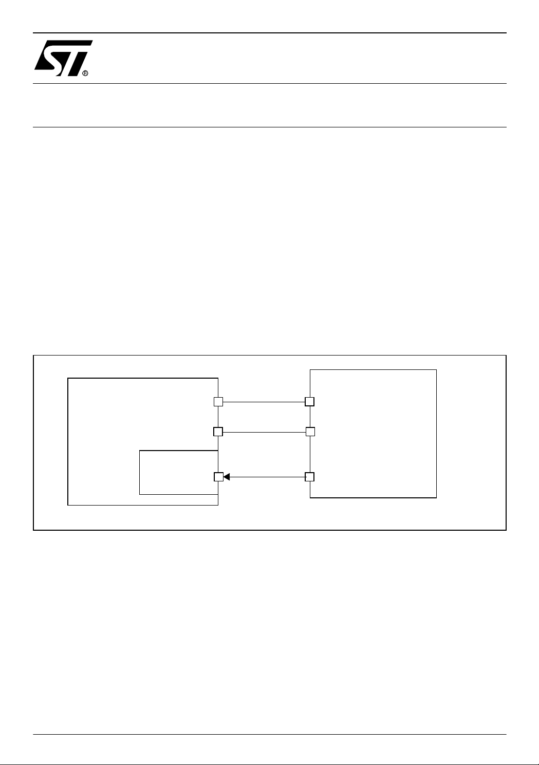
2 ST7 / KEYBOARD INTERFACE
Connect the analog keyboard to one of the analog inputs of the ST 7 and connect the high and
low voltage references as shown in Figure 1.
Figure 1. ST7 / keyboard interface set-up
KEYBOARD
ST7
ADC
V
DD
V
SS
analog
input
AINx
high voltage reference
low voltage reference
keyboard
output
3 ST72324 CONFIGURATION
The application has been tested with a ST72F324 configured as described below. Refer to the
datasheet for more details on configuring the ST72F324.
3.1 I/O CONTROL
Depending on the num ber of pins av ailable on the device p ackage , th e S T7 theor etically allows up to 16 multiplexed analog inputs to the ADC, but in practice, on the ST72F324 device,
there can be up to 12 analog inputs. They are alternate functions I/O Port D (PD0-PD5), Port
AN979/0303 1/14
1
Page 2
DRIVING AN ANALOG KEYBOARD WITH THE ST7 ADC
F (PF0, PF4), and Port C (PC0, PC1, PC5, PC7). The I/O port pins used by the ADC must be
configured as floating inputs to avoid conflicts in alternate function mode.
Refer to the Data Sheet for information on configuring the I/O ports.
3.2 ANALOG TO DIGITAL CONVER TER
The ST7 ADC is a 10-bit successive approximation converter, with internal sample and holdcircuitry.
3.2.1 ADC control
You control the ADC using the ADC Control Status Register (ADCCSR).
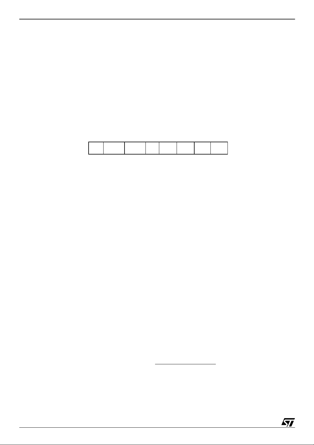
CH0CH1CH2CH30ADONSPEEDEOC
The EOC bit is the end of conversion bit:
- When this bit is set, the conversion is done and result can be read from the ADC
Data Registers (ADCDRL & ADCDRH).
- When the bit is reset, the conversion is not complete.
The SPEED bit:
- When this bit is set, f
ADC
- When this bit is reset, f
= f
ADC
CPU
= f
/ 2.
CPU
/ 4.
The ADON bit:
- Enable ADC and start conversion when this bit is set.
- Disable ADC and stop conversion when this bit is reset.
CH3-CH0 bits:
- They are used to s elect which analog i nput to convert. In the ST72324 there are 12
analog pins.
3.2.2 Characteristics
The conversion time is 15 ADC cycles including a sampling time of 4 ADC cycles.
The ADC is linear and the digital result of the conversion is given by the formula:
1023*Input Voltage
Digital Result =
Reference Voltage
3.2.3 Process
First the analog input pins must be configured as floating inputs (see Section 3.1).
2/14
Page 3
DRIVING AN ANALOG KEYBOARD WITH THE ST7 ADC
Then the analog channel to c onvert must be s elected using CH3-CH0 bits of ADCCSR regsister.
Then select the SPEED of conversion.
Setting the ADON bit will switch the converter on.
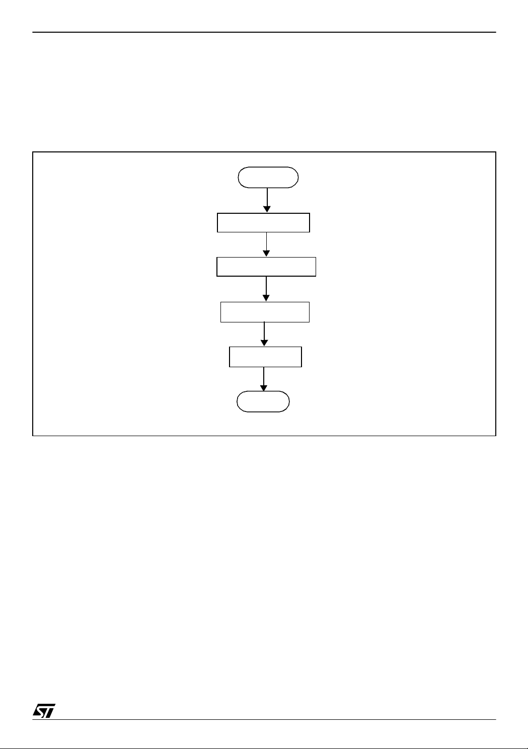
Figure 2. Flowchart: initialization of the ADC
KBD_init
I/O Initialization
Channel Selection
SPEED Selecti on
ADC ON
return
Once a conversion is done, the EOC bit is set by hardware. It will be r eset when the ADCDRH
register is read.
Once enabled, conversions will run continuously until the peripheral is disabled.
3/14
Page 4
DRIVING AN ANALOG KEYBOARD WITH THE ST7 ADC
Figure 3. Flowchart: conversion process
Conversion Process
KBD_init
no
EOC = 1 ?
yes
read ADCDRL
read ADCDRH
4 ANALOG KE YBOARD
4.1 PRINCIPLE
The purpose is to recognize a key when pressed. In an analog keyboard each key is associated with a voltage. The description of an analog keyboard is given by Figure 4.
Figure 4. Hardware description of a keyboard with 16 keys
V
DD
V
key
(Keyboard Value)
R
up
R
0
key 0
key 1
R
1
Σ
with R
is a pull-up resistor. So, when no key is pressed, V
R
up
4/14
>> R
j
up
R
13
R
14
key 14
key 15
is equal to VDD.
key
V
SS
Page 5

DRIVING AN ANALOG KEYBOARD WITH THE ST7 ADC
When ‘key i’ is pressed (where i is in the range 1 to 15), the resistor R
is connected to Vss.
i-1
Then we have a resistive divider
and V
is given by the formula:
key
V
key i
=
(V
DD
R
- VSS)
+
up
i - 1
Σ
j = 0
i - 1
Σ
j = 0
R
R
j
j
So the corresponding voltage of each key i s given by the values of the r esistor s. An equal distribution of voltage between V
To recognize a key, the user will measure V
and VSS is usually recommended.
DD
and will be able to decide which key was
key
pressed.
4.2 PRACTICAL LIMITATIONS
Theoretic ally, wi th an 10- bit ADC , 1023 key s can be decod ed. But po tenti al erro rs must be
taken into account. They can come from the power supply, the key resistivity, the resistor tolerance, the ADC conversion errors.
The resistor toleran ce is the m ain limitati on as us ually 5% tole rance res istors a re us ed. It i s
advised to use a 1% tolerance resistor for the pull-up. Changing this resistor greatly improves
the keyboard as the pull-up has an influence on every key.
The AD C t otal u nad justed e rr or (T UE ) for th e devi ce is spec ifi ed a s 4 LS B. S o, it h as t o be
taken into account to avoid any key decision error.
These parameters will reduce the number of keys that can be efficiently decoded.
5/14
Page 6
DRIVING AN ANALOG KEYBOARD WITH THE ST7 ADC
5 KEY DETECTI ON
The ST7 is a digital microcontroller. It uses its ADC to measure V
. It is then coded in 10 bits.
key
As the ADC is linear, the best decision is taken when the voltage levels of the keys follow an
equal distribution between V
In our application, a 16-key keyboard is used. So, the best associated V
and VSS.
DD
value of ‘key i’ is
key
given by:
(VDD - VSS) * i
V
=
key i
16
The problem is that you cannot choose the perfect values for the resistors. In our application,
the following resistor values were used (see Table 1):
Table 1. Exam ple of resistor values for 16 keys
Resistor Value (Ω) Resistor Value (Ω)
R
up
R0 68 R8 270
R1 75 R9 390
1K R7 220
R2 82 R10 560
R3 100 R11 820
R4 120 R12 1K2
R5 150 R13 2K7
R6 180 R14 75
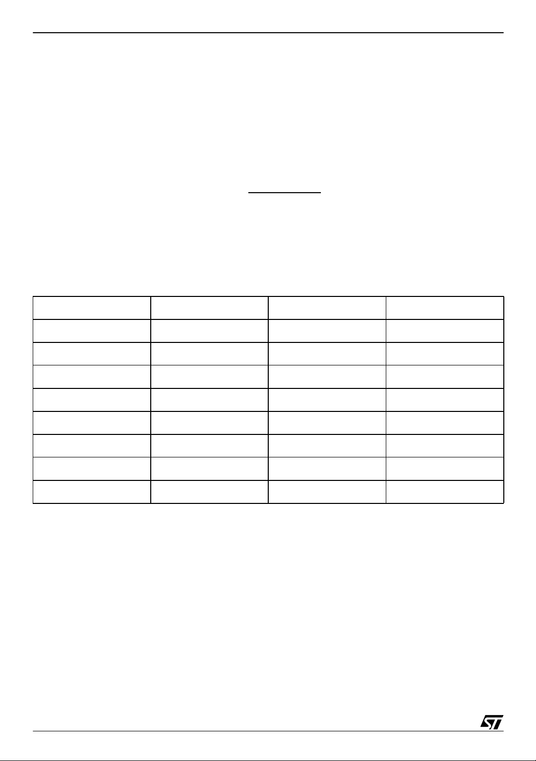
The digital values of the keys after conversion are given in Table 2.
When a key is pressed and after conversion, a decision must be taken on its value. Upper and
lower limits of the detection for each key must be defined. These values are the middle of two
subsequent typical values, which gives the best noise margin between keys.
The software uses the lower limits to make its decision. They are given in Table 2.
6/14
Page 7

Ta ble 2. Key Values
DRIVING AN ANALOG KEYBOARD WITH THE ST7 ADC
KEY
no key 0x3FF 0x3DF
‘F’ 0x3C0 0x38E ‘7’ 0x1C0 0x1A0
‘E’ 0x37E 0x35E ‘6’ 0x17 E 0x1 5E
‘D’ 0x33D 0x31D ‘5’ 0x13C 0x11C
‘C’ 0x303 0x2E3 ‘4’ 0x0FB 0x0DB
‘B’ 0x2C2 0x2A2 ‘3’ 0x0BC 0x09C
‘A’ 0x27E 0x25E ‘2’ 0x080 0x060
‘9’ 0x23D 0x 21D ‘1’ 0x041 0x021
‘8’ 0x200 0x1E 0 ‘0’ 0x000 0x000
typical digital
valu e
lower digi t al
limit of KEY
KEY
typical di gi t al
value
lower digital
limit o f KEY
7/14
Page 8

DRIVING AN ANALOG KEYBOARD WITH THE ST7 ADC
6 DRIVING AN ANALOG KE YBOARD WITH THE ST7 ADC
The complete software is provided in an attached zip file (in assembly & C using ST7 software
library version 1.1) to this application note. It is only an example. It is up to the user to adapt it
to the application.
6.1 GENERAL DE SCRIPTION
A 16-key keyboard is connected to the ST72F324 through the AIN0 pin on Port D.
A LED is connected to an output pin (PC0) to indicate to the user that a key is detected.
Figure 5. Application circuitry
output
LED
ST7
V
SS
V
DD
V
ADC
DD
analog
input
R
up
R
0
R
14
key 0
key 15
V
SS
The software uses a polling strategy. It makes conversions continuously (no wake-up
process).
First the software initializes the I/Os and the ADC.
When a conversion is done, the software decides if a key was pressed or not.
If not, it waits before analyzing the result of a new conversion.
If a key is pressed, it compares it with the former key to know if the key is stabilized. Then, a
LED is switched on.
8/14
Page 9

DRIVING AN ANALOG KEYBOARD WITH THE ST7 ADC
6.2 FLOWCHARTS
The main flowcharts of the application are given below in Figure 6, Figure 7 & Figure 8. The initialization routine is presented in Figure 2.
Figure 6. Flowchart: main program
MAIN
KBD_init
KBD_val
KBD_process
wait
9/14
Page 10

DRIVING AN ANALOG KEYBOARD WITH THE ST7 ADC
Figure 7. Flowchart: key detection
KBD_val
no
EOC = 1?
yes
disable interrupt
Y = ADCDRL (D1, D0)
A = ADCDRH (D9 - D2)
enable interrupt
Converted
yes
X = Offset for Lower
Digital Limit of Key ‘F’
Digital value (A,Y) >=
Specified Lower Digital
limit of Key ‘9’
no
X = Offset for Lower
Digi t a l Li mi t o f K e y ‘ 8 ’
Conv er te d
Digital value (A,Y) >=
Specified Lower Digital
limit of NO_KEY
Reduce the Offset
for Next Lower Key
yes
X = NO_KEY
no
+
Converted Digital
no
value (A,Y) >= Specified
Lower Digital limit of Key
(pointed by offset)
+
yes
X = Keyval
return
10/14
Page 11

DRIVING AN ANALOG KEYBOARD WITH THE ST7 ADC
Figure 8. Flowchart: key process
key_process
X = FF ?
no
X = Preval?
no
LED glows
Preval = X
return
yes
yes
11/14
Page 12

DRIVING AN ANALOG KEYBOARD WITH THE ST7 ADC
6.3 EXTENSION FOR WAKE UP
With the ST7, it is possible to generate a wake-up function. This can be achieved by a mod-ification of the circuit. T he pul l-up resistor mu st be c onnected to an ad ditional port pin. Dur ing
key poll ing, this p in is in o utput m ode and act ive h i gh, t hus s witchi ng V
to the pull-up re-
DD
sistor.
Figure 9. Keyboard with wake-up circuitry.
ST7
V
SS
I/0
R
ADC
analog
input
AINx
up
R
0
key 0
R
14
key 15
V
SS
During the wait for a key to be pressed, the I/O pin used for the pull-up is switched into a high
impedance state (e.g. open drain output mode). The pin used as the ADC input while polling
is switched to interrupt input with pull-up mode.
So if any key is presse d an interrupt will be ge nerated if the voltag e at this pin i s below th e
Schmitt trigger low level threshold. The serial resistors in the keyboard chain must not be too
high in this case, therefore the maximum number of key s i s reduced in comparison to normal
mode.
12/14
Page 13

DRIVING AN ANALOG KEYBOARD WITH THE ST7 ADC
6.4 SOFTWARE
All the source files in assembly code as well as in C code are given in the zip file with this application note. The C code uses software library (ST7 software library version 1.1).
The source files are for guidance only. STMicroelectronics shall not be held liable for any direct, indirect or consequential damages with respect to any claims arising from use of this s oftware.
13/14
Page 14

DRIVING AN ANALOG KEYBOARD WITH THE ST7 ADC
THE PRESENT NOTE WHICH IS FOR GUIDANCE ONLY AIMS AT PROVIDING CUSTOMERS WITH INFORMATION
REGARDING THE IR PRO DUCT S IN OR DER FO R THEM TO SAV E TIME . AS A RES ULT, STMIC ROEL ECTR ONI CS
SHALL NOT BE HELD LIABLE FOR ANY DIRECT, INDIRECT OR CONSEQUENTIAL DAMAGES WITH RESPECT TO
ANY CL AIM S AR IS IN G FR OM T HE CO N TENT OF S UC H A NO TE A ND /O R T HE U SE M AD E BY C US TO ME RS O F
THE INFORMATION CONTAINED HEREIN IN CONNECTION WITH THEIR PRODUCTS.”
Information furnished is believed to be accurate and reliable. However, STMicroelectronics assumes no responsibility for the consequences
of use of such information nor for any infringement of patents or other rights of third parties which may result from its use. No license is granted
by implic ation or otherwise under any patent or patent ri ghts of STM i croelectr oni cs. Spec i fications mentioned i n this publication are subje ct
to change without notice. This publication supersedes and replaces all information previously supplied. STMicroelectronics products are not
authorized for use as cri tical comp onents in life support dev i ces or systems wi thout the express written approv al of STMicroel ectronics.
The ST logo is a registered trademark of STMicroelectronics
2003 STMicroelectronics - All Rights Reserved.
STMicroelectronics Group of Compan i es
http://www.s t. com
Purchase of I
2
C Components by STMicroelectronics conveys a license under the Philips I2C Patent. Rights to use the se components in an
2
I
C system i s granted pro vi ded that the sy stem conforms to the I2C Standard Specification as defined by Philips.
Australi a - B razil - Canada - China - Finl and - France - Germany - Hong Kong - Ind ia - Israel - Italy - Japan
Malaysi a - M al ta - Morocco - Singapore - Spain - Sw eden - Switz erland - United Kingdom - U.S.A.
14/14
 Loading...