

Page 1

AN977
APPLICATION NOTE
GUIDELINES FOR UPGRADING FROM THE ST92F120
(0.50 µm) TO THE ST92F124/F150/F250 (0.35 µm)
by Microcontroller Division Applications
INTRODUCTION
Microcontroll ers for emb edd ed app licat ions tend to int egra te mo re a nd mo re p eriphe ral s as
well as larger memories. Providing the right products with the right features such as Flash, emulated EEPROM and a wide range of peripherals at the right cost is always a challenge. That
is why it is mandatory to shrink the microcontroll er die size regularly as soon as the technology
will allow it. This major step applies to the ST92F120.
The purpose of this document is to present the differences between the ST92F120 microcontroller in 0.50 micron technology versus the ST92F124/F150/F250 in 0.35 micron technology.
It provides some guidelines for upgrading applications for both its software and hardware aspects.
In the first part of this document, the differences between the ST92F120 and ST92F124/F150/
F250 devices are listed. In the second part, the modifications required for the application hardware and software are described.
AN977/0203 1/17
1
Page 2
GUIDELINES FOR UPGRADING FRO M THE ST92F120 (0.50 µm) TO TH E ST92F124...
1 UPGRADING FROM THE ST92F120 TO THE ST92F124/F150/F 250
ST92F124/F150/F250 microcontrollers using 0.35 micron technology are similar to ST92F120
microcon trollers using 0.50 mi cron tec hnolo gy, but s hrinki ng is used to add s ome ne w features and to improve th e p erforma nce s of ST 92F1 24/F15 0/F 250 d evic es. A lm ost a ll p eripherals keep the same features, which is why this document focuses only on the modified sections. If there is no difference between the 0.50 micron peripheral compared to the 0.35 one,
other than its technology and design methodology, the peripheral is not presented. The new
analog to digital converter (ADC) is the m ajor change. This ADC uses a single 16 channel A/
D converter with 10 bits resolution instead of two 8-channel A/D converters with 8-bit resolution. The new memory organization, ne w rese t and clock control unit, internal voltage regulators and new I/O buffers will almost be transparent changes for the application. The new peripherals are the Controller Area Network (CAN) and the asynchronous Serial Communication
Interface (SCI-A).
1.1 PINOUT
The ST92F124/F150/F250 was designed in order to be able to replace the ST92F120. Thus,
pinouts are nearly the same. The few differences are described below:
– Clock2 was remapped from port P9.6 to P4.1
– Analog input channels were remapped according to the table below.
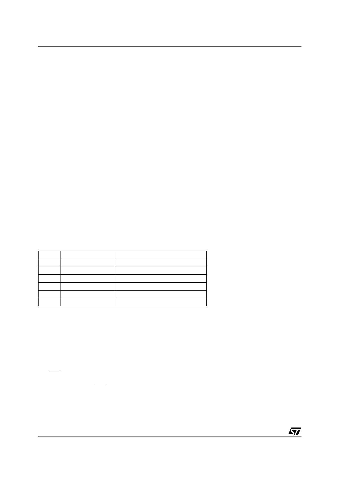
Table 1. Analog Input Channel Mapping
PIN ST92F120 Pinout ST92F124/F150/F250 Pinout
P8.7 A1IN0 AIN7
... ... ...
P8.0 A1IN7 AIN0
P7.7 A0IN7 AIN15
... ... ...
P7.0 A0IN0 AIN8
– RXCLK1(P9.3), TXCLK1/ CLKOUT1 (P9.2), DCD1 (P9.3), RTS1 (P9.5) were removed be-
cause SCI1 was replaced by SCI-A.
– A21(P9.7) down to A16 (P9.2) were added in order to be able to address up to 22 bits exter-
nally.
– 2 new CAN peripheral devices are available: TX0 and RX0 (CAN0) on ports P5.0 and P5.1
and TX1 and RX1 (CAN1) on dedicated pins.
1.2 RW
Under Reset state, RW
RESET STATE
is held high with an internal weak pull-up wher eas it was not on the
ST92F120.
2/17
2
Page 3
GUIDELINES FOR UPGRADING FROM THE ST92F120 (0.50 µm) TO THE ST92F124...
1.3 SCHMITT TRIGGERS
– I/O ports with Special Schmitt Triggers are no longer present on the ST92F124/F150/F250
but are replaced by I/O ports with High Hysteresis Schmitt Triggers. The related I/O pins are:
P6[5-4].
– Differences on the VIL and VIH. See Table 2.
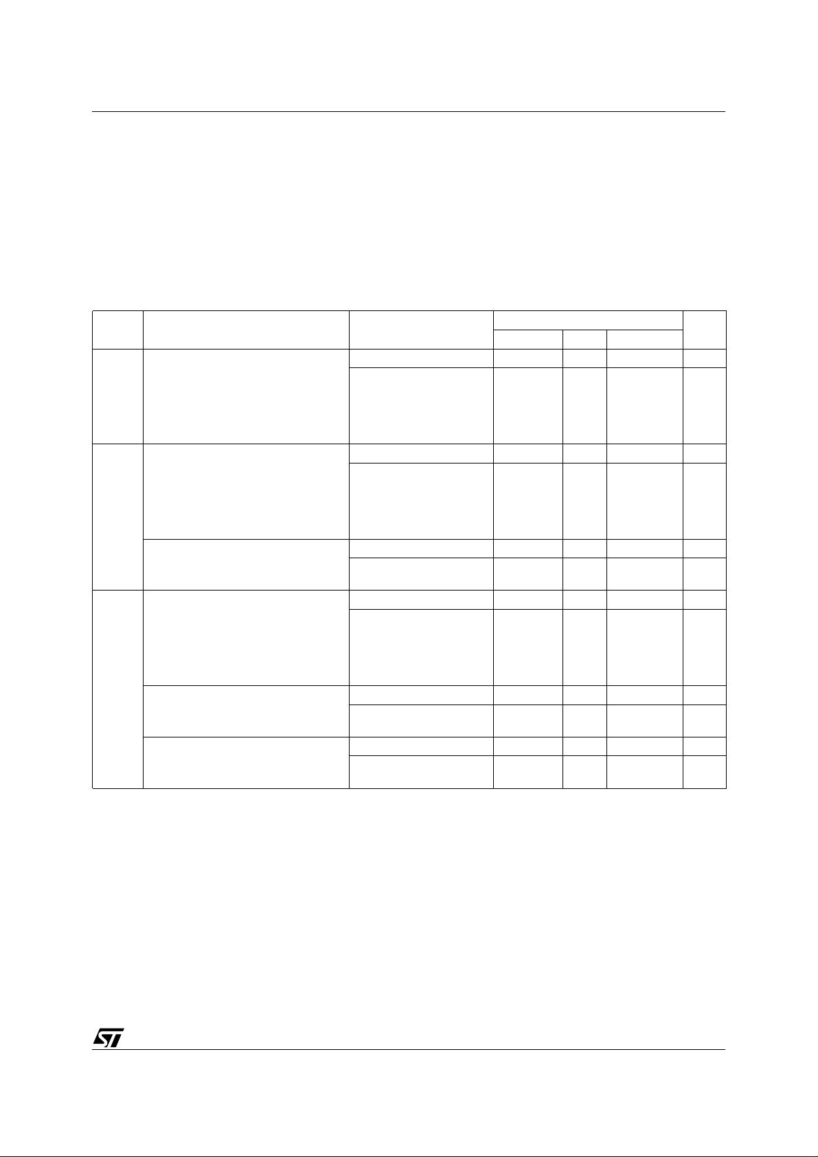
Table 2. Input Level Schmitt Trigger DC Electrical Characteristics
(VDD = 5 V ± 10%, TA = –40° C to +125° C, unless otherwise specified)
Symbol Parameter Device
ST92F120 0.7 x V
ST92F124/F150/F250 0.6 x V
ST92F120 0.8 V
ST92F124/F150/F250 0.2 x V
ST92F120 0.3 x V
ST92F124/F150/F250 0.25 x V
ST92F120 600 mV
ST92F124/F150/F250 250 mV
ST92F120 800 mV
ST92F124/F150/F250 1000 mV
ST92F120 900 mV
ST92F124/F150/F250 1000 mV
V
V
V
HYS
Input High Level
Standard Schmitt Trigger
P2[5:4]-P2[1:0]-P3[7:4]-P3[2:0]-
IH
P4[4:3]-P4[1:0]-P5[7:4]-P5[2:0]P6[3:0]-P6[7:6]-P7[7:0]-P8[7:0]P9[7:0]
Input Low Level
Standard Schmitt Trigger
P2[5:4]-P2[1:0]-P3[7:4] P3[2:0]P4[4:3]-P4[1:0]-P5[7:4]-P5[2:0]P6[3:0]-P6[7:6]-P7[7:0]-P8[7:0]-
IL
P9[7:0]
Input Low Level
High Hyst.Schmitt Trigger
P4[7:6]-P6[5:4]
Input Hysteresis
Standard Schmitt Trigger
P2[5:4]-P2[1:0]-P3[7:4]-P3[2:0]-
P4[4:3]-P4[1:0]-P5[7:4]-P5[2:0]P6[3:0]-P6[7:6]-P7[7:0]-P8[7:0]P9[7:0]
Input Hysteresis
High Hyst. Schmitt Trigger
P4[7:6]
Input Hysteresis
High Hyst. Schmitt Trigger
P6[5:4]
Value
Min Typ
DD
DD
(1)
Max
DD
DD
DD
Unit
V
V
V
V
V
(1)
Unless otherwise stated, typical data are based on TA= 25°C and VDD= 5V. They are only reported
for design guide lines not tested in production.
1.4 MEMORY ORGANIZATION
1.4.1 External memory
On the ST92F120, only 16 bits were externally available. Now, on the ST92F124/F150/F250
device, the 22 b its o f th e MM U are exter nally avai lable. This o rgani zation is used to mak e it
3/17
Page 4

GUIDELINES FOR UPGRADING FRO M THE ST92F120 (0.50 µm) TO TH E ST92F124...
easier to address up to 4 external Mbytes. But segments 0h to 3h and 20h to 23h are not externally available.
1.4.2 Flash Sector Organization
Sectors F 0 to F3 ha ve a ne w organi zatio n in the 12 8K and 60K Fl ash dev ices as s hown in
Table 5 and Table 6. Table 3. and Table 4 show the previous organization.
Table 3. Memory Structure for 128K Fla sh ST92F120 Flash Device
Sector Addresses Max Size
TestFlash (TF) (Reserved) 230000h to 231F7Fh 8064 bytes
OTP Area
Protection Registers (reserved)
Flash 0 (F0) 000000h to 00FFFFh 64 Kbytes
Flash 1 (F1) 010000h to 01BFFFh 48 Kbytes
Flash 2 (F2) 01C000h to 01DFFFh 8 Kbytes
Flash 3 (F3) 01E000h to 01FFFFh 8 Kbytes
EEPROM 0 (E0) 228000h to 228FFFh 4 Kbytes
EEPROM 1 (E1) 22C000h to 22CFFFh 4 Kbytes
Emulated EEPROM 220000h to 2203FFh 1 Kbyte
231F80h to 231FFBh
231FFCh to 231FFFh
124 bytes
4 bytes
Table 4. Memory Structure for 60K Flas h ST92F120 Flash Device
Sector Addresses Max Size
TestFlash (TF) (Reserved) 230000h to 231F7Fh 8064 bytes
OTP Area
Protection Registers (reserved)
Flash 0 (F0) 000000h to 000FFFh 4 Kbytes
Reserved 001000h to 00FFFFh 60 Kbytes
Flash 1 (F1) 010000h to 01BFFFh 48 Kbytes
Flash 2 (F2) 01C000h to 01DFFFh 8 Kbytes
EEPROM 0 (E0) 228000h to 228FFFh 4 Kbytes
EEPROM 1 (E1) 22C000h to 22CFFFh 4 Kbytes
Emulated EEPROM 220000h to 2203FFh 1Kbyte
231F80h to 231FFBh
231FFCh to 231FFFh
Table 5. Memory Structure for 128K ST 92F124/F150/F250 Flash device
Sector Addresses Max Size
TestFlash (TF) (Reserved) 230000h to 231F7Fh 8064 bytes
OTP Area
Protection Registers (reserved)
Flash 0 (F0) 000000h to 001FFFh 8 Kbytes
Flash 1 (F1) 002000h to 003FFFh 8 Kbytes
Flash 2 (F2) 004000h to 00FFFFh 48 Kbytes
Flash 3 (F3) 010000h to 01FFFFh 64 Kbytes
231F80h to 231FFBh
231FFCh to 231FFFh
124 bytes
4 bytes
124 bytes
4 bytes
4/17
Page 5

GUIDELINES FOR UPGRADING FROM THE ST92F120 (0.50 µm) TO THE ST92F124...
Sector Addresses Max Size
Hardware Emulated EEPROM sec-
tors
(reserved)
Emulated EEPROM 220000h to 2203FFh 1 Kbyte
228000h to 22CFFFh 8 Kbytes
Table 6. Memory Structure for 64K ST 92F124/F150/F250 Flash device
Sector Addresses Max Size
TestFlash (TF) (Reserved) 230000h to 231F7Fh 8064 bytes
OTP Area
Protection Registers (reserved)
Flash 0 (F0) 000000h to 001FFFh 8 Kbytes
Flash 1 (F1) 002000h to 003FFFh 8 Kbytes
Flash 2 (F2) 004000h to 00BFFFh 32 Kbytes
Flash 3 (F3) 010000h to 013FFFh 16 Kbytes
Hardware Emulated EEPROM sec-
tors
(reserved)
Emulated EEPROM 220000h to 2203FFh 1 Kbyte
231F80h to 231FFBh
231FFCh to 231FFFh
228000h to 22CFFFh 8 Kbytes
124 bytes
4 bytes
Since the user reset vector location is set at address 0x000000, the application can use sector
F0 as an 8-Kbyte user bootloader area, or sectors F0 and F1 as a 16-Kbyte area.
1.4.3 Flash & E
In order to save a data po inter register (DPR), the Flash and E
control registers are remapped from page 0x89 to page 0x88 where the E
cated. Thi s way, only one DPR is us ed to poi nt to both the E
2
E
PROM control registers. But the registers are still accessible at the previous address. The
3
PROM Control Register Location
3
PROM (Emulated E2PROM)
3
PROM area is lo-
3
PROM variabl es and Flas h &
new register addresses are:
– FCR 0x221000 & 0x224000
– ECR 0x221001 & 0x224001
– FESR0 0x221002 & 0x224002
– FESR1 0x221003 & 0x224003
In the application, these register locations are usually defined in the linker script file.
5/17
Page 6

GUIDELINES FOR UPGRADING FRO M THE ST92F120 (0.50 µm) TO TH E ST92F124...
Fi
ST92F120 I
ill
Fi
ST92F124/F150/F250 I
ill
1.5 RESET AND CLOC K CONTROL UNIT (RCCU)
1.5.1 Oscillator
A new low power oscillator is implemented with the following target specifications:
– Max. 200 µamp. consumption in Running mode,
– 0 amp. in Halt mode,
gure 1.
OSCOUT
OSCIN
nternal Osc
ator
HALT
CLOCK
BUFFER
REF
INPUT
gure 2.
R
POL
OSCIN
I
LOAD
nternal Osc
V
DD
ator
CLOCK1
VR02086A
OSCOUT
1.5.2 PLL
One bit (bit7 FREEN) has been added to the PLLCONF register (R246, page 55), this is to enable Fre e Runn ing mode . The r eset value for th is re gister is 0x0 7. Wh en th e FREE N b it is
reset, it has the same behaviour as in the ST92F120, meaning that the PLL is turned off when:
– entering stop mode,
– DX(2:0) = 111 in the PLLCONF register,
– entering low power modes (Wait For Interrupt or Low Power Wait for Interrupt) foll owing the
WFI instruction.
When the FREEN bit is set and any of the conditions listed above occur, the PLL enters Free
Running mode, and oscillates at a low frequency which is typically about 50 kHz.
In addition, when the PLL provides the internal clock, if the clock signal disappears (for instance du e to a bro ken or disc onnect ed res onat or...), a s afety c loc k sig nal is au tomat icall y
provided, allowing the ST9 to perform some rescue operations.
The frequency of this clock signal depends on the DX[0..2] bits of the PLLC ONF register
(R246, page55).
Refer to the ST92F124/F150/F250 datasheet for more details.
6/17
Page 7

GUIDELINES FOR UPGRADING FROM THE ST92F120 (0.50 µm) TO THE ST92F124...
1.6 INTERNAL VOLTAGE REGULATOR
In the ST92F124/F150/F250, the cor e operates at 3.3V, while the I/Os still operate at 5V. In
order to supply the 3.3V power to the core, an internal regulator has been added.
Actually, this voltage regulator consists of 2 regulators:
– a main voltage regulator (VR),
– a low power voltage regulator (LPVR).
The main voltage regu lator (VR) supp lies the current requir ed by the device in all operating
modes. The voltage regulator (VR) is stabilized by adding an external capacitor (300 nF minimum) on one of the two Vreg pins. These Vreg pins are not able to drive other external devices, and are only used for regulating the internal core power supply.
The low power voltage regulator (LPVR) generates a non-stabilized voltage of approximately
VDD/2, with minimum internal static dissipation. The output current is limited, so it is not sufficient for full device operation mode. It provides reduced power consumption when the chip is
in Low Power mode (Wait For Interrupt, Low Power Wait For Interrupt, Stop or Halt modes).
When the VR is active, the LPVR is automatically deactivated.
1.7 EXTENDED FUNCTION TIMER
The hardware modifications in the Extended F unction Tim er of the ST92F124/ F150/F250 as
compared to the ST92F120 only concern the interrupt generation functions. But some specific
information has been added to the documentation concerning Forced Compare mode and
One Pulse mode. This information may be found in the updated ST92F124/F150/F250 Datasheet.
1.7.1 Input Capture/Output Compare
On the ST92F124/F150/F250, the IC1 and IC2 (OC1 and OC2) interrupts can be enabled separately. This is done using 4 new bits in the CR3 register:
– IC1IE=CR3[7]: Input Capture 1 Interrupt Enable. If reset, Input Capture 1 interrupt is inhibit-
ed. When set, an interrupt is generated if the ICF1 flag is set.
– OC1IE=CR3[6]: Output Co mpare 1 Interrupt Enable. When reset, Output Compare 1 inter-
rupt is inhibited. When set, an interrupt is generated if the OCF2 flag is set.
– IC2IE=CR3[5]: Input Capture 2 Interrupt Enable. When reset, Input Capture 2 interrupt is in-
hibited. When set, an interrupt is generated if the ICF2 flag is set.
– OC2IE=CR3[4]: Output Co m pare 2 Interr upt Enable. When reset, Output Compare 2 Inter-
rupt is inhibited. When set, an interrupt is generated if the OCF2 flag is set.
Note: The IC1IE and IC2IE (OC1IE and OC2IE) interrupts are not significant if the ICIE (OCIE)
is set. In order to be taken into account, the ICIE (OCIE) must be reset.
7/17
Page 8

GUIDELINES FOR UPGRADING FRO M THE ST92F120 (0.50 µm) TO TH E ST92F124...
1.7.2 PWM Mode
The OCF1 bit cannot be set by hardware i n PWM mode, but the OCF2 bit i s set every time the
counter matches the value in the OC2R register. This can generate an interrupt if the OCIE is
set or if the OCIE is reset and OC2IE is set. This interrupt will help any application where pulse
widths or periods need to be changed interactively.
1.8 A/D CONVERTER (ADC)
A new A/D converter with the following main features has been added:
– 16 channels,
– 10-bit resolution,
– 4 MHz maximum frequency (ADC clock),
– 8 ADC clock cycles for sampling time,
– 20 ADC clock cycle for conversion time,
– Zero input reading 0x0000,
– Full scale reading 0xFFC0,
– Absolute accuracy is ± 4 LSBs.
This new A/D converter has the same architec ture as the previous one. It s till s upports the analog watchdog feature, but now it uses only 2 of the 16 channels. T hese 2 channels are contiguous and channel addresses can be selected by software. With the previous solution using
two ADC cells, four analog watchdog channels w ere availabl e but at fixed channel addresses,
channels 6 and 7.
Refer to the updated ST92F124/F150/F250 Datasheet for the description of the new A/D Converter.
1.9 I²C
1.10 I²C IERRP BIT RESET
On the ST92F124/F150/F250 I²C, the IERRP (I2CISR) bit can be reset by s oftware even if one
of the following flags is set:
– SCLF, ADDTX, AF, STOPF, ARLO and BERR in the I2CSR2 register
– SB bit in the I2CSR1 Register
It is not true for the ST92F120 I²C: the IERRP bit cannot be reset by software if one thes e flags
is set. For this reason, on the ST92F120, the corresponding interrupt routine (entered following a first event) is re-entered i mmediately if another event occ urred during the fi rst routi ne
execution.
8/17
Page 9

GUIDELINES FOR UPGRADING FROM THE ST92F120 (0.50 µm) TO THE ST92F124...
1.10.1 START EVENT REQU EST
A difference between the ST92F120 and the ST92F124/F150/F250 I²C exists on the START
bit generation mechanism.
To generate a START event, the application code sets the START and ACK bits in the I2CCR
register:
– I2CCCR |= I2Cm_START + I2Cm_ACK ;
Without the compiler opti mization opti on selected, it is transl ated in assem bler the following
way:
– or R240,#12
– ld r0,R240
– ld R240,r0
The OR instruction sets the Start bit. O n the ST 92F124/F150/F250, the s econd load instruction executi on re sults in a s econ d S TAR T ev ent r e quest . Th is seco nd STA RT e vent occu rs
after the next byte transmission.
With any of the comp iler op timization options selected, the assembler code does not request
a second START event:
– or R240,#12
1.11 NEW PERIPHERALS
– Up to 2 CAN (Controller Area Network) cells have been added. Specifications are available
in the updated ST92F124/F150/F250 Datasheet.
– Up to 2 SCIs are available: the SCI-M (Multi-protocol SCI) is the same as on the ST92F120,
but the SCI-A (Asynchronous SCI) is new. The specifications for this new peripheral are
available in the updated ST92F124/F150/F250 Datasheet.
9/17
Page 10

GUIDELINES FOR UPGRADING FRO M THE ST92F120 (0.50 µm) TO TH E ST92F124...
2 HARDWARE & SOFTWARE MODIFICATIO NS TO THE APPLICATION BOARD
2.1 PINOUT
– Due to its remapping, CLOCK2 can not be used in the same application.
– SCI1 can only be used in asynchronous mode (SCI-A).
– The modifications of the analog input channels mapping can be easily handled by software.
2.2 INTERNAL VOLTAGE REGULATOR
Due to the presence of the internal voltage regulator, external capacitors are required on the
Vreg pins in order to provide the core with a stabilized power supply. In the ST92F124/F150/
F250, the core operates at 3.3V, while the I/Os still operate at 5V. The minimum recommended value is 600 nF or 2*300 nF and the distance between the Vreg pins and the capacitors must be kept to a minimum.
No other modifications need to be made to the hardware application board.
2.3 FLASH & EEPROM CONTROL REGISTERS AND MEMORY ORGANIZATION
To save 1 DPR, the symbo l address definition s that corr espond to th e Flash an d EEPRO M
control registers can be modified. This is generally done in the li nker script file. T he 4 registers,
FCR, ECR, and FESR[0:1], have been defined at 0x221000, 0x221001, 0x221002 and
0x221003, respectively.
The 128-Kbyte Flash sector reor ganization also affe cts the l inker script file. It m ust be modi fied in compliance with the new sector organization.
Refer to Section 1.4.2 for the description of the new Flash sector organization.
2.4 RESET AND CLOC K CONTROL UNIT
2.4.1 Oscillator
2.4.1.1 Crystal Oscillator
Even if the compatibility with the ST92F120 board design is maintained, it is no longer recommended to insert a 1MOhm resistor in parallel with the external crystal oscillator on a
ST92F124/F150/F250 application board.
10/17
Page 11

GUIDELINES FOR UPGRADING FROM THE ST92F120 (0.50 µm) TO THE ST92F124...
Figure 3. ST92F120 Cry s tal Oscillator Figure 4. ST92F150 Crystal Oscillator
CRYSTAL CLOCK
CRYSTAL CLOCK
ST9
ST9
OSCIN
C
1
*Recommended for oscillator stability
OSCOUT
C
1 MΩ *
2
VR02116A
OSCIN
C
1
*Rd can be inserted to reduce the drive level,
when using low drive crystals.
OSCOUT
Rd
*
C
2
2.4.1.2 Leakages
While the ST92F120 is sensitive to leakage from GND to OSCIN, the ST92F124/F1 50/F250
is sensitive to leakage from VDD to OSCIN. It is recommended to surround the crystal oscillator by a ground ring on the printed circuit board and to apply a coating film to avoid humidity
problems, if necessary.
2.4.1.3 External clock
Even if compatibility with the ST9 2F120 board design is maintained, it is recomm ended to
apply the external clock on the OSCOUT input.
The advantages are:
– a standard TTL input signal can be used whereas the ST92F120 Vil on the external c lock is
between 400mV and 500mV.
– the external resistor between OSCOUT and VDD is not required.
Figure 5. ST92F120 External Clock Figure 6. ST92F150 External Clock
3.3 k
INPUT
CLOCK
EXTERNAL CLOCK
Ω
OSCOUT
ST9
OSCIN
VR02116B
INPUT
CLOCK
EXTERNAL CLOCK
OSCIN
ST9
OSCOUT
VR02116B
11/17
Page 12

GUIDELINES FOR UPGRADING FRO M THE ST92F120 (0.50 µm) TO TH E ST92F124...
2.4.2 PLL
2.4.2.1 Standard Mode
The reset value of the PLLCONF register (p55, R246) will start the application in the same way
as in the ST92F120. To use free running mode in the conditions described in Section 1.5, the
PLLCONF[7] bit must be set.
2.4.2.2 Safety Clock Mode
Using the ST92F120, if the clock signal disappears, the ST9 core and peripheral clock is
stopped, nothing can be done to configure the application in a safe state.
The ST92F124/F 150/F25 0 design int roduces the sa fety clock signal , the applicati on can be
configured in a safe state.
When the clock signal d isappea rs (fo r instan ce due to a brok en or disconne cted r esonato r),
the PLL unlock event occurs.
The safer way to manage this event is to enable the INTD0 external interrupt and to assign it
to the RCCU by setting the INT_SEL bit in the CLKC TL register.
The associated interrupt routine chec ks the interrupt source (refer to the 7.3.6 Interrupt Generation Chapter of the S T92F 124/F150/F250 data shee t), and config ures the applica tion in a
safe state.
Note: The peripheral clock is not stopped and any external signal gener ated by the microcontroller ( for inst anc e P WM, ser ial c o mmu nic atio n.. .) mu st b e s toppe d duri ng the f irst in str uctions executed by the interrupt routine.
2.5 EXTENDED FUNCTION TIMER
2.5.1 Input Capture / Output Com pare
In order to generate a Timer Interrupt, a program developed for the ST92F120 may need to be
updated in certain cases:
– If Timer Interrupts IC1 and IC2 (OC1 and OC2) are both used, ICIE (OCIE) of register CR1
has to be set. The value of the IC1IE and IC2IE (OC 1 IE and OC2IE) in the CR3 register is
not significant. So, the program does not have to be modified in this case.
– If only one Interrupt is needed, ICIE (OCIE) must be reset and IC1IE or IC2IE (OC1IE or
OC2IE) must be set depending on the interrupt used.
– If none of the Timer Interrupts are used, ICIE, IC1IE and IC2IE (OCIE, OC1IE and OC2IE)
they must all be reset.
12/17
Page 13

GUIDELINES FOR UPGRADING FROM THE ST92F120 (0.50 µm) TO THE ST92F124...
2.5.2 PWM Mode
A Timer Interrupt can now be generated each time Counter = OC2R:
– To enable it, set OCIE or OC2IE,
– To disable it, reset OCIE AND OC2IE.
2.6 10-BIT ADC
Since the new ADC is entirely different, the program will have to be updated:
– All data registers are 10 bits, which includes the threshold registers. So each register is di-
vided into two 8-bit registers: an upper regist er and a lower register, in which only the 2 most
significant bits are used:
Table 7. DiHR
70
Di.9 Di.8 Di.7 Di.6 Di.5 Di.4 Di.3 Di.2
Table 8. DiLR
70
Di.1Di.0000000
– The start conversion channel is now defined by bits CLR1[7:4] (Pg63, R252).
– The analog watchdog channels are selected by bits CLR1[3:0]. The only condition is that the
two channels must be contiguous.
– The ADC clock is selected with CLR2[7:5] (Pg63, R253).
– Interrupt registers have not been modified.
Because of the increased length of ADC registers, the register map is different. The location of
the new registers is given in the description of the ADC in the updated ST92F 124/F150/F250
Datasheet.
2.7 I²C
2.7.1 IERRP BIT RESET
In the ST92F124/F150/F250 interrupt routine dedicated to the Error Pending event (IER RP is
set), a software loop must be implemented.
This loop checks every flag and executes the c orresponding needed ac tions. The loop will not
end until all flags are reset.
At the end of thi s softwa re loop exe cution , the IER RP bit is reset by so ftware an d the co de
exits from the interrupt routine.
13/17
Page 14

GUIDELINES FOR UPGRADING FRO M THE ST92F120 (0.50 µm) TO TH E ST92F124...
2.7.2 START Event Request
To avoid any unwanted double START event, use any of the compiler otpimization options, in
the Makefile.
For instance:
CFLAGS = -m$(MODEL) -I$(INCDIR) - O3 -c -g -Wa,-alhd=$*.lis
14/17
Page 15

GUIDELINES FOR UPGRADING FROM THE ST92F120 (0.50 µm) TO THE ST92F124...
3 UPGRADING AND RECONFIGURING YOUR ST9 HDS2V2 EMULATOR
3.1 INTRODUCTION
This sectio n conta ins inform ation about ho w to upgrad e your em ulat or’s firmw are or rec onfigure it to support a ST92F150 probe. Once you have reconfigured your emulator to support
a ST92F150 probe you can configure it back to support an other probe (for example a
ST92F120 probe) following the same procedure and choosing the suitable probe.
3.2 PREREQUISITES TO UPGRADING AND/OR RECONFIGURING YOUR EMULATOR
The following ST9 HDS2V2 emulators and emulation probes support upgrades and/or reconfiguration with new probe hardware:
– ST92F150-EMU2
– ST92F120-EMU2
– ST90158-EMU2 and ST90158-EMU2B
– ST92141-EMU2
– ST92163-EMU2
Before trying to perform the upgrade/recon figuration of your emulator, you must ensure that
ALL of the following conditions are met:
– The monitor version of your ST9-HDS2V2 emulator is higher than or equal to 2.00. [You can
see which monitor version your emulator has in the Target field of the About ST9+ Visual
Debug window, which you open by selecting Help>About.. from the ST9+ Visual Debug’s
main menu.]
– If your PC is running on the Windows ® NT ® operating system, you must have the admin-
istrator privileges.
– You must have installed the ST9+ V6.1.1 (or later) Toolchain on the host PC connected to
your ST9 HDS2V2 emulator.
15/17
Page 16

GUIDELINES FOR UPGRADING FRO M THE ST92F120 (0.50 µm) TO TH E ST92F124...
3.3 HOW TO UPGRADE/RECONFIGURE YOUR ST9 HDS2V2 EMULATOR
The procedure tells you how to upgrade/reconfigure your ST9 HDS2V2 emulator. Be sure you
meet all the prerequisites before starting, otherwise you could damage your emulator by performing this procedure.
1.Ensure that your ST9 HDS2V2 emulator is connected via the parallel port to your host PC
running either Windows ® 95, 98, 2000 or NT ®. If you are reconfiguring your emulator to
be used with a new probe, the new probe must be physically connected to the HDS2V2
main board using the three flex cables.
2. On the host PC, from Windows ®, select Start >Run....
3.Click the Browse button to browse to folder where you installed the ST9+ V6.1.1 Toolchain.
By default, the installation folder path is C:\ST9PlusV6.1.1\... In the installation folder,
browse to the ..\downloader\ subfolder.
4. Locate the ..\downloader\<ST9xxxx-EMU2>\ directory corresponding to the name of the
emulator you want to upgrade/configure.
For example, if you want to reconfigure your ST92F120 emulator to be used with the
ST92F150-EMU2 emulation probe, browse to the ..\downloader\<ST92F150-EMU2>\
directory.
5.Then select the directory corresponding to the version you wish to install (for example, the
V1.01 version is found in ..\downloader\<ST92F150-EMU2>\v1.01\) and select the file
<setup_st9xxxx.bat> (for example, setup_st92f150.bat).
6.Click on Open.
7.Click OK in the Run window. The update will begin. You have simply to follow the instruc-
tions displayed on your PC’s screen.
WARNING: Do no t stop the emulat or, or the pr ogram w hile the upd ate is in progress ! Your
emulator may be damaged!
16/17
Page 17

GUIDELINES FOR UPGRADING FROM THE ST92F120 (0.50 µm) TO THE ST92F124...
“THE PRESENT NOTE WHICH IS FOR GUIDANCE ONLY AIMS AT PROVIDING CUSTOMERS WITH INFORMATION
REGARDING THE IR PRO DUCT S IN OR DER FO R THEM TO SAV E TIME . AS A RES ULT, STMIC ROEL ECTR ONI CS
SHALL NOT BE HELD LIABLE FOR ANY DIRECT, INDIRECT OR CONSEQUENTIAL DAMAGES WITH RESPECT TO
ANY CLAIMS ARISING FROM THE CONTENT OF SUCH A NOTE AND/OR THE USE MADE BY CUSTOMERS OF
THE INFORMATION CONTAINED HEREIN IN CONNECTION WITH THEIR PRODUCTS.”
Information furnished is believed to be accurate and reliable. However, STMicroelectronics assumes no responsibility for the consequences
of use of such information nor for any infringement of patents or other rights of third parties which may result from its use. No license is granted
by implic ation or otherwise under any patent or patent r i ght s of STMi croelectr oni cs. Spec i fications mentione d i n this publicatio n are subj ect
to change without notice. This publication supersedes and replaces all information previously supplied. STMicroelectronics product s are not
authorized for use as cri tical comp onents in lif e support devi ces or systems without the express written appr oval of STMic roelectronics.
The ST logo is a registered trademark of STMicroelectronics
2003 STMicroelectronics - All Rights Reserved.
STMicroelectronics Grou p of Companies
http://www.s t. com
Purchase of I
2
C Components by STMicroelectronics conveys a license under the Philips I2C Patent. Rights to use the se components in an
2
C system i s granted pro vi ded that the sy stem conforms to the I2C Standard Specification as defined by Philips.
I
Australi a - Brazil - Canada - China - Fi nl and - Franc e - Germany - Hong Kong - Ind i a - Is rael - Ital y - J apan
Malaysi a - M al ta - Morocco - Singapore - Spain - Sweden - Sw itzerland - Uni t ed Kingdo m - U.S.A.
17/17
 Loading...