

Page 1

AN971
APPLICATION NOTE
I2C COMMUNICATION BETWEEN
ST7 AND M24Cxx EEPROM
by Microcontroller Division Applications
INTRODUCTION
The goal of this application note is to present an practical example of communication using the
2
C peripheral of the ST7. It shows a basic single master communication between a ST7 mi-
I
crocontroller and an M24C xx I
through the I
ment.
2
C interface, a write and a read to the external EEPROM without error manage-
2
C bus EEPROM. T he purpose i s to i mplem ent, from the ST7
AN971/0403 1/7
1
Page 2
I2C COMMUNICATION BETWEEN ST7 AND M24Cxx EEPROM
1 ST7 I2C INTERF ACE
The ST7 I2C peripheral allows multi master and slave communication with bus error management. In this application, only single master mode is used without error management. As
polling mode i s the mos t d ifficult m ode to i mplemen t, t he applicati on is base d o n th is mo de,
but it can be easily adapted for interrupt management.
2
The I
(Serial data line). The corresponding port pins have to be configured as floating inputs.
Please refer to the ST7 datasheet for more details.
1.1 COMMUNICATION SPEED
The ST7 I
standard and fast I
In master mode the communication speed is given by the Clock Control Register (CCR). An
example is given in Table 1.
C synchronous communication needs only two signals: SCL (Serial clock line) and SDA
2
C peripheral allows a large range of com mun ication spee ds. It is ab le to work in
2
C modes.
2
Table 1. Example of Possible I
Speed [KHz] 15.5 25.00 50.00 70.00 100.00 167.00 190.00 333.00
CCR [hex] EC 9E 4E 37 26 8E 8C 86
C Communication Speeds (f
Standar d Mo de Fast Mod e
CPU
=8 MHz)
1.2 START, STOP CONDITION AND ACKNOWLEDGE GENERATION
In master mode, the Start and Stop c ondition s can be generated by setting the START and
STOP bits in the Control Register (CR).
An Acknowledge is sent after an address or a data byte is received when the ACK bit is set in
the Control Register (CR).
2/7
2
Page 3
I2C COMMUNICATION BETWEEN ST7 AND M24Cxx EEPROM
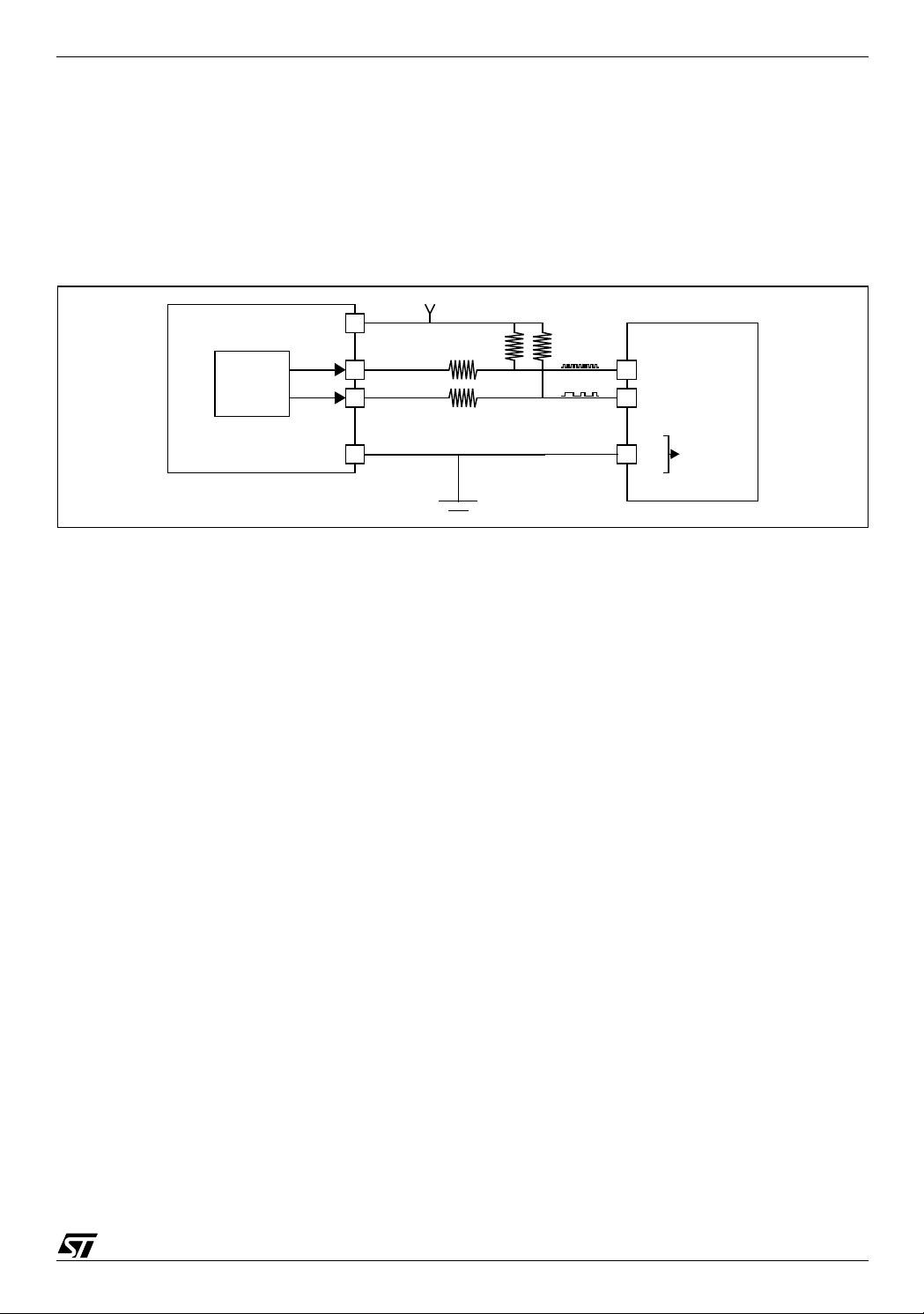
2 ST7 / M24CXX I2C COMMUNICATION APPLICA T ION
2.1 HARDWARE CONFIGURATION
2
The ST7 / M24Cxx I
troller which communicates with an external M24C08 EEPROM through an I
Figure 1. ST7 / EEPRO M I2C Communications Application
C communication application hardware consists of a ST72264 microcon-
5V
V
SCL
SDA
DD
2x27KΩ
2x100Ω
M24C08
SCL
SDA
ST72264
I2C
2
C bus interface.
V
SS
2.2 ST7 I
In this chapter all registers refer to the ST7 I
2.3 INITIALIZE THE I
2
C PERIPHERAL BASIC DRIVERS
2
C PERIPHERAL
2
C peripheral (unless otherwise specified).
In this ap plicati on th e i nitial ization o f the ST7 I
2
C peripheral is done comp letely by softw are
E
Address=A0h
without taking into account the hardware reset status.
First the Control Register (CR) is cleared and the Data (DR) and Status (SR1,SR2) registers
are touched to clear any pending events.
Then, the peripheral is enabled through the Control Register (CR) . This action needs to write
twice in the register due to the fact that the Control Register (CR) bits can be set only when the
PE enab le bi t is alre ady set. To allow the pe riph eral to ack nowl edge th e re ceive d dat a the
ACK bit of the Control Register (CR) is set.
2
As the ST24C08 EEPROM is specified with a maximum I
2
I
C peripheral is set to this speed (CCR=26h) in the application.
C clock speed at 100KHz, the ST7
3/7
Page 4

I2C COMMUNICATION BETWEEN ST7 AND M24Cxx EEPROM
2.4 INITIATING A COM MUNICATION ON THE I2C BUS
2
To initiate an I
C communication, first a start condition has to be generated and then the se-
lected slave address has to be sent, both by the master.
2
In the ST7 I
C peripheral this action is done by setting the START bit of the Control Register
(CR) followed by writing the slave address in the Data Register (DR) with the least significant
bit correctly set (0 = transmission, 1 = reception).
2
2.5 SENDING A DATA BYTE ON THE I
To transmit a new data byte from the ST7 I
C BUS
2
C peripheral on the I2C bus, the address or data
byte pre v iou sly t ran sm itted ha s to b e com pl ete d c orre ctl y. Th is p re vio us byt e t ran smi ss ion
check is done by a pol ling loop on the B TF flag o f the Status Regi ster 1 (S R1). If dur ing this
loop an error is detected in the Status Registers (SR1,SR2) then the application goes into an
infinite loop (no error management).
When the prev ious dat a t ransmis sion is over, the app lication w rites the new data by te to be
transmitted in the Data Register (DR).
Note: If the data byte to be transmitted is the first one after the slave address, a dummy write
in the Control Register (CR) has to be performed to allow the setting of the BTF bi t (see ST7
datasheet for more details). In this application, this dummy w rite is done by setting the PE bit
for each data byte transmission (see description of EV6 in the Transfer Sequencing diagram
2
C datasheet description).
in I
2
2.6 RECEIVING A DATA BYTE ON THE I
To receive a new data byte in the ST7 I
C BUS
2
C peripheral from the I2C bus, the data byte to receive
has to be completed correctly. This byte reception check is done by a polling loop on the BTF
flag of the Status Register 1 (SR1). If during this loop an error is detected in the Status Registers (SR1, SR2) then the application goes in an infinite loop (no error management).
When the data reception is finalized, the application reads the new data by te received in the
Data Register (DR).
To close the communication: Before reading the last byte from the DR register, set the STOP
bit to generate the Stop condition. The interface goes automatically back to slave m ode (M/
SL bit cleared). In order to generate the non-acknowledge pulse after the last received data
byte, the ACK bit must be cleared just before reading the second last data byte.
Note: If the data byte to be received is the first one after the slave address, a dummy write in
the Control Register (CR) has to be performed to allow the setting of the BTF bit (see ST7 datasheet for more details). In this application, this dummy write is done by setting the PE bit for
2
each data byte reception (see des cription of EV6 i n the Transfer Sequenc ing diagram i n I
C
datasheet description).
4/7
Page 5

I2C COMMUNICATION BETWEEN ST7 AND M24Cxx EEPROM
2.7 COMMUNICATING WITH THE I2C EEPROM
The communication protocol between the ST7 and the external M24Cxx EEPROM is given in
Figure 2. For more details, please refer to the ST24C08 datasheet.
2
Figure 2. I
C Communication Protocol
Write data from ST7 to EEPROM
EEPROM @ SUB @
START
ACK
ACK
DATA 1
ACK
DATA 2
DATA N-1 DATA N STOP
ACK
ACK
Read data from EEPROM to ST7
START
EEPROM @
EEPROM @
ACK
SUB @ ACK DATA 1 ACK DATA N NACK
START
ACK
STOP
The ST7 / M24Cxx communication application is based on two steps:
– Write the content of an output buffer (from the ST7 ROM) in the M24Cxx EEPR OM
– Read this written buffer from the M24Cxx EEPROM to the ST7 RAM.
Figure 3. shows the flowchart of these two steps.
Figure 3. Communication Application Flowchart
Write data from ST7 to EEPROM Read data from EEPROM to ST7
INITIATE TRANSMISSION
(START + SLAVE @)
SEND SUB @ DATA
INITIATE TRANSMISSION
(START + SLAVE @)
SEND SUB @ DATA
INITIATE RECEPTION
(START + SLAVE @ with LSB set)
END OF
yes
BUFFER
no
no
2nd LAST DATA
TO RECEIVE
yes
SEND NEXT BUFFER DATA
SET THE STOP CONDITION BIT
CLEAR ACKNOWLEDGE BIT
no
LAST DATA
TO RECEIVE
yes
SET THE STOP CONDITION BIT
RECEIVE NEXT BUFFER DATA
no
END OF
RECEPTION
yes
5/7
Page 6

I2C COMMUNICATION BETWEEN ST7 AND M24Cxx EEPROM
3 SOFTWARE
All the source files in assembly code are given in zip file with this application note.
The source files are for guidance only. STMicroelectronics shall not be held liable for any di-
rect, indirect or consequential damages with respect to any claims arising from use of this s oftware.
To adapt this polling software to interrupt management, replace the polling waiting loop by an
interrupt event.
6/7
Page 7

I2C COMMUNICATION BETWEEN ST7 AND M24Cxx EEPROM
“THE PRESENT NOTE WHICH IS FOR GUIDANCE ONLY AIMS AT PROVIDING CUSTOMERS WITH INFORMATION
REGARDING THE IR PRO DUCT S IN OR DER FO R THEM TO SAV E TIME . AS A RES ULT, STMIC ROEL ECTR ONI CS
SHALL NOT BE HELD LIABLE FOR ANY DIRECT, INDIRECT OR CONSEQUENTIAL DAMAGES WITH RESPECT TO
ANY CL AIM S AR IS IN G FR OM T HE CO N TENT OF S UC H A NO TE A ND /O R T HE U SE M AD E BY C US TO ME RS O F
THE INFORMATION CONTAINED HEREIN IN CONNECTION WITH THEIR PRODUCTS.”
Information furnished is believed to be accurate and reliable. However, STMicroelectronics assumes no responsibility for the consequences
of use of such information nor for any infringement of patents or other rights of third parties which may result from its use. No license is granted
by implic ation or otherwise under any patent or patent ri ghts of STM i croelectr oni cs. Specifications mentioned in thi s publicati on are subject
to change without notice. This publication supersedes and replaces all information previously supplied. STMicroelectronics products are not
authorized for use as cri tical comp onents in life support dev i ces or systems wi thout the express written approv al of STMicroel e ctronics.
The ST logo is a registered trademark of STMicroelectronics
2003 STMicroelectronics - All Rights Reserved.
STMicroelectronics Group of Compan i es
http://www.s t. com
Purchase of I
2
C Components by STMicroelectronics conveys a license under the Philips I2C Patent. Rights to use the se components in an
2
C system i s granted pro vid ed that the sy stem conforms to the I2C Standard Specification as defined by Philips.
I
Australi a - Brazil - Canada - China - Fi nl and - France - Germany - Hong Kong - India - Israel - I taly - Japan
Malaysi a - M al ta - Morocco - Singapore - Spain - Sw eden - Switz erland - United Kingdom - U.S.A.
7/7
 Loading...