

Page 1

AN970
APPLICATION NOTE
SPI COMMUNICATION BETWEEN ST7 AND EEPROM
by 8-Bit Micro Application Team
INTRODUCTION
The goal of this application note is to present a practical example of communication using the
SPI peripheral of the ST7.
It shows an easy way of communicating between a ST7 microcontroller and a M95xxx SPI
EEPROM. The purpose is to perform, through SPI, a write in the m em ory, follow ed by a read
of the written data.
AN970/0802 1/10
1
Page 2
SPI COMMUNICATION BETWEEN ST7 AND EEPROM
1 ST7 / EEPROM SPI INTERFACE
This section summarizes the main features of the ST7/EEPROM SPI interface. Please refer to
the ST7 datasheet for more details.
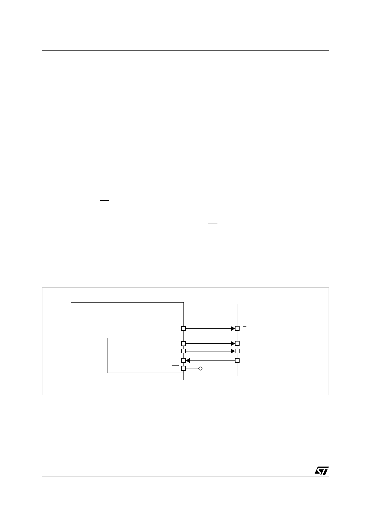
The Serial Pe ripheral Int erface (S PI) allows full-duplex , synchr onous, se rial commu nicati on
between devices. A SPI system may consist of a master and several slaves, or of a system in
which devices may be either master or slave.
There is only one master at any one time.
The Bus signals are:
- The s erial cloc k (SCK).
- The MOSI (Master Out Slave In).
- The MISO (Master In Slave Out).
One more pin, the SS
pin (slave select), is needed to select the slave or the master mode for
each device. this can be done in hardware or software mode.
In this application the ST7 is always used as master (SS
pin = high level) and configures the
EEPROM mode through an output. The ST7 and SPI interface set-up is shown Figu re 1.
During SPI transfer, data is simultaneously transmitted (shifted out serially) and received
(shifted in serially). Data are transmitted MSB first. The serial clock is used to synchronize the
data transfer during a sequence of eight clock pulses.
Figure 1. ST7 and SPI Interface Set-Up
EEPROM
ST7
SPI Interface
I/O
SCK
MOSI
MISO
SS
VCC
S
C
D
Q
M95040
2/10
2
Page 3
SPI COMMU NICATION BETWEEN ST7 AND EEPR OM
2 ST72264 CONFIGURATION
2.1 I/O CONTROL
Four pins of the ST72264 are used:
- The 3 data and clock SPI pins (SCK, MOSI, MISO ).
- An output pin to select and deselect the M95xxx.
pin to select master or slave mode.
- SS
In our application, the output for selecting the M95xxx is pin 3 of Port B. It is configured as
output push-pull (refer to the datasheet for details).
2.2 SPI PERIPHERAL
2.2.1 General
This peripheral is configured with the SPI Control Register.
70
SPIE SPE SPR2 MSTR CPOL CPHA SPR1 SPR0
The output must be enabled (SPE = 1).
If the SS
pin is high (s ee SP ICSR) , the ST 722 64 can be declar ed as m aste r by sett ing the
MSTR bit.
The transmission speed, in master mode, is selected using the SPR0, SPR1 and SPR2 bi ts.
The CPOL and CPHA bits define the timing characteristics.
When the SPIE bit is set, SPI interrupts are enabled (not used in our case).
2.2.2 SS
The SS
software configuration
pin can be fixed by hardware, either connected to Vss (for a slave configuration) or to
Vdd (for a master configuration). But it can also be software driven through the SPICSR register (SSM and SSI bits) :
70
SPIF WCOL OVR MODF - SOD SSM SSI
To set the master configuration (as in our case) : SSM=1 and SSI=1
To set the slave configuration: SSM=1 and SSI=0
3/10
Page 4

SPI COMMUNICATION BETWEEN ST7 AND EEPROM
2.2.3 Baud rates
First the communication speed must be chosen. As the clock is given by the master, the user
has to configure the baud rate of the ST7 SPI (SPR[2-0] bits in the SPICR register).
For each CPU frequency, six Baud Rates are available. If f
= 8MHz, the baud rate range is
CPU
62.5kHz to 2MHz.
2.2.4 Clock phase and polarity
Then the clock polarity and the clock phase have to be chosen.
The clock polarity (CPOL bit of the SPCR register) controls the steady state value of the clock
when no data is being transferred.
The clock phase (CPHA bit of the SPCR register) s elects on whic h clock transition the bit cap-
ture is made and consequently on which clock transition data is latched.
The user must be careful of the fact that s ome devices do not allow all ti ming relationships. For
instance, the ST95040 EEPROM device accepts only CPOL,CPHA = (0,0) or (1,1) configurations.
4/10
Page 5

SPI COMMU NICATION BETWEEN ST7 AND EEPR OM
3 M95040 EEPROM MANAGEMENT AND CONFIGURATION
3.1 MAIN FEATURES
This is a 4K memory composed of two pages of 2K bytes.
All instructions, addresses and data are shifted in and out of the chip MSB first.
The write protect pin (W
) and the hold pin (H) are not us ed in ou r appli cation ( both a re hi gh
level).
3.2 STATUS REGISTER
This device has one status register.
The BP1 and BP0 bits in the status register can be used to write protect a block of memory. In
this application, both bits are cleared, allowing write access to all the memory.
The WEL bit indicates the status of the write enable latch.
The WIP bit indicates whether the memory is busy with a write operation.
3.3 INSTRUCTION SET
Prior to any operation, the device must be selected (SS
pin at low level), then an one-byte instruction code must be sent to the EEPROM. The device has a set of 6 instructions (see Table
1 Instruction Set).
Table 1. Instruction Set
Instructio n Descripti on Instructio n fo rmat
WREN Set Write Enable Latch 0000 0110
WRDI Reset Write Enable Latch 0000 0100
RDSR Read Status Register 0000 0101
WRSR Write Status Register 0000 0001
READ Read Data from Memory Array 0000 A
WRITE Write Data to Memory Array 0000 A
Notes: A8 = 1, Upper page selected.
A
= 0, Lower page selected.
8
8
8
011
010
5/10
Page 6

SPI COMMUNICATION BETWEEN ST7 AND EEPROM
4 ST7 / EEPROM SPI PROTOCOL
The use of the main functions are briefly described below. For a complete description of the
protocol, please refer to the M95040 SPI EEPROM data sheet.
Write_enable: The memory contains a w r ite enable l atch. T his latch must be set prior to any
WRITE or WRSR operation.
Byte_write: This function will write up to 16 bytes of data i n the EEPROM. After the WRITE instruction, the memory address must be specified before sending data.
Byte_read: This function reads the memory. After the READ instruction, the memory address
is specified. To be able to send the dat a, the EEPROM m ust receive the clock fr om the
master: the ST7. T his is made by s ending a du mmy byte. T his operation w ill generate the 8
clock bits needed. The dummy value will not be seen by the EEPROM.
Write_SR: Give the proper value to the Status Register prior to any comm unication.
Read_SR: This process is sim ilar to the byte read process. It will be used to check if ther e is
a write in progress (WIP bit of the status register).
5 SPI COMMUNICATION BETWEEN AN ST7 AND AN EEPROM
The software included with this application note is only the SPI driver. The complete software
can be found in the software library in the ST internet website. It i s of course only an example.
It is up to the user to adapt it to his specific application.
5.1 GENERAL DE SCRIPTION
The software is a polling SPI communication between the ST72264 and EEPROM.
The first part of the software performs to the initialization of the ST72264 (core and SPI periph-
eral) and of the EEPROM (value of status register for no protection).
Then it executes the write cycles. The «write_loop» writes in the EEPROM (16 bytes at a time
for optimization), the values 0 to 111 from the address 0 up to 111.
The third part executes the read cycles. The «read_loop» reads the content of the EEPROM
at a time from address 0 up to 111.
Finally, the software ends in an infinite loop.
6/10
Page 7

SPI COMMU NICATION BETWEEN ST7 AND EEPR OM
5.2 HARDWARE DESCRIPTION
Two components were used for the application:
- 1 ST72264 MCU
- 1 M95040 EEPROM
Figure 2. Hardware description
110pF
1
V
S
CC
Q
W
V
V
V
SS
SS
CC
H
C
D
M95040
V
CC
V
CC
SS (soft driven)
SCK
MISO
MOSI
PB3
ST72264
pin of ST72264 is software driven (high state for a master device).
SS
The SCK pin is connected to the serial clock pin (C) of the E²PROMs.
The MOSI pin to the serial input pins (D).
The MISO pin to the serial output pins (Q).
pin of the EEPROM is connected to the PB3 output pin of ST72264.
S
V
CC
V
SS
V
CC
V
SS
5.3 FLOWCHARTS
The flowchart of the application is presented below (Figure 3).
7/10
Page 8

SPI COMMUNICATION BETWEEN ST7 AND EEPROM
Figure 3. Flowchart: MAIN
MAIN
initialization
clear X and A
write_enable
byte_write
X at address A
read_SR
yes
write in progress?
no
increment address A by 16
no
end of writing?
(x=111)
yes
clear X and A
byte_read
at address A
increment X
no
end of reading?
(x=111)
8/10
yes
END
Page 9

SPI COMMU NICATION BETWEEN ST7 AND EEPR OM
5.4 USE OF SEVERA L EEPROMS
It is possible to communicate with several EEPROMs. Each one is selected in turn. Then the
same protocol as described before is followed.
The main point is to reserve one I/O p in to select each device.
A hardware schematic using two devices is given below (Figure 4).
The selection of the devices is made using the PB2 and PB3 pins.
Figure 4. Hardware schematic for two devices
110pF
1
V
S
CC
Q
W
V
V
V
SS
SS
CC
H
C
D
M95040
110pF
V
S
CC
Q
W
V
V
V
SS
CC
H
C
SS
D
M95040
V
CC
V
CC
V
CC
V
CC
SS(soft driven)
SCK
MISO
MOSI
PB3
PB2
ST72264
V
CC
V
SS
V
CC
V
SS
5.5 SOFTWARE
All the source files in assembly code are given in the zip file with this application note.
The source files are for guidance only. STMicroelectronics shall not be held liable for any di-
rect, indirect or consequential damages with respect to any claims arising from use of this s oftware.
9/10
Page 10

SPI COMMUNICATION BETWEEN ST7 AND EEPROM
“THE PRESENT NOTE WHICH IS FOR GUIDANCE ONLY AIMS AT PROVIDING CUSTOMERS WITH INFORMATION
REGARDING THE IR PRO DUCT S IN OR DER FO R THEM TO SAV E TIME . AS A RES ULT, STMIC ROEL ECTR ONI CS
SHALL NOT BE HELD LIABLE FOR ANY DIRECT, INDIRECT OR CONSEQUENTIAL DAMAGES WITH RESPECT TO
ANY CLAIMS ARISING FROM THE CONTENT OF SUCH A NOTE AND/OR THE USE MADE BY CUSTOMERS OF
THE INFORMATION CONTAINED HEREIN IN CONNECTION WITH THEIR PRODUCTS.”
Information furnished is believed to be accurate and reliable. However, STMicroelectronics assumes no responsibility for the consequences
of use of such information nor for any infringement of patents or other rights of third parties which may result from its use. No license is granted
by implic ation or otherwise under any patent or patent ri ghts of STM i croelectr oni cs. Specifications mentioned in thi s publicati on are subject
to change without notice. This publication supersedes and replaces all information previously supplied. STMicroelectronics products are not
authorized for use as cri tical comp onents in life support dev i ces or systems wi thout the express written approv al of STMicroel e ctronics.
The ST logo is a registered trademark of STMicroelectronics
2002 STMicroelectronics - All Rights Reserved.
STMicroelectronics Group of Compan i es
http://www.s t. com
Purchase of I
2
C Components by STMicroelectronics conveys a license under the Philips I2C Patent. Rights to use the se components in an
2
C system i s granted pro vid ed that the sy stem conforms to the I2C Standard Specification as defined by Philips.
I
Australi a - Brazil - Canada - China - Fi nl and - France - Germany - Hong Kong - India - Israel - I taly - Japan
Malaysi a - M al ta - Morocco - Singapore - Spain - Sw eden - Switz erland - United Kingdom - U.S.A.
10/10
 Loading...