

Page 1
AN966
®
APPLICATION NOTE
L6561, ENHANCED TRANSITION MODE
POWER FACTO R CORR ECT O R
by Claudio Adragna
The TM (Transition Mode) technique is widely used for Power Factor Correction in low power applications, such as lamp ballasts or low-end monitors. The L6561 is the latest ST’s proposal for this
market and the emerging ones that are supposed to require a low-cost Power Factor Correction.
Based on a well-established architecture, the L6561 offers excellent performance that enla rges its
field of application considerably.
Introduction
The front-end stage of conventional off -line converters, typically made up of a full wave rectifier bridge
with a capacitor filter, gets an unregulated DC bus from the AC mains. The filter capacitor must be large
enough to have a relat ively low ripple superimposed on the DC level. This means that the instantaneous
line voltage is below the voltage on the capacitor most of the time, thus the rectifiers conduct only for a
small portion of each line half-cycle. The current drawn from the mains is then a series of narrow pulses
whose amplitude is 5-10 times higher than the resulting DC value.
Lots of drawbacks result f r om that : much higher peak and RMS current drawn from the line, distortion of
the AC line voltage, overcurrents in the neutral line of the three-phase systems and, after all, a poor utilisation of the power system’s energy capability.
This can be measured in terms of either harmonic contents, as norms EN61000-3-2 envisage, or Power
Factor (PF), intended as the rat io between the real power (the one transferred to the output) and the apparent power (RMS line voltage times RMS line current) drawn from the mains, which is more immediate. A traditional input stage with capacitive filter has a low PF (0.5-0.7) and high harmonic contents.
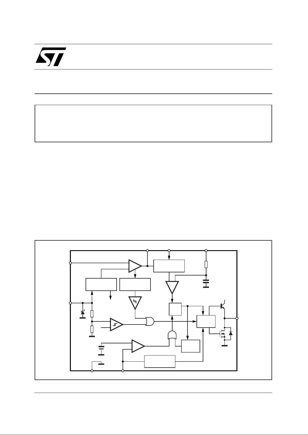
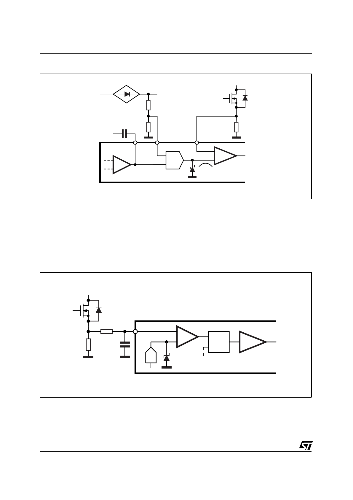
Figure 1. Internal Block Diagram of the L6561.
1
INV
V
VOLTAGE
REGULATOR
8
CC
20V
R2
2.1V
1.6V
6
GND
INTERNAL
SUPPLY 7V
R1
V
REF2
+
-
-
2.5V
+
OVER-VOLTAGE
DETECTION
UVLO
ZERO CURRENT
+
-
5
ZCD
DETECTOR
COMP MULT CS
23 4
MULTIPLIER
+-
RSQ
DISABLE
40K
5pF
DRIVER
STARTER
D97IN547D
V
CC
7
GD
March 2003
1/21
Page 2

AN966 APPLICATION NOTE
By using switching techniques, a Power Factor Corrector (PFC) preregulator, located between the rectifier bridge and the filter capacitor, allows drawing from the mains a quasi-sinusoidal current, in-phase
with the line voltage. The PF becomes very close to 1 (more than 0.99 is possible) and the aforesaid
drawbacks are eliminated.
Theoretically, any switching topology can be used to achieve a high PF but, in practice, the boost topology has become the most popular because of the advantages it offers:
1) mainly, the circuit requires the fewest external parts, thus it is the cheapest. Additionally:
2) the boost induct or located between the bridge and the switch causes the input di/dt t o be low, thus
minimizing the noise generated at the input and, therefore, the requirements on the input EMI filter;
3) the switch is source-grounded, therefore is easy to drive.
However, boost topology requires the DC output voltage to be higher than the maximum expected line
peak voltage (400VDC is a typical value for 220V or wide range mains applications). Besides, there is no
isolation between input and output, thus any line voltage surge will be passed on to the output.
Two methods of controlling a PFC preregulator are currently widely used: the fixed frequency average
current mode PWM and the Transition Mode (TM) PWM (fixed ON-time, variable frequency). The first
method needs a complex control that requires a sophisticated controller IC (ST’s L4981A, with the variant of the frequency modulation of fered by the L4981B) and a consi derable component count. The second one requires a simpler control (implemented by ST’s L6561), much fewer external parts and is
therefore much less expensive.
With the first method the boost inductor works in continuous conduction mode, while TM makes the inductor work on the boundary between continuous and discontinuous mode, by definition. For a given
throughput power, TM operation then involves higher peak currents. This, also consistently with cost
considerations, suggests its use in a lower power range (typically below 150W), while t he former is recommended for higher power levels.
L6561 PFC controller Integrated Circuit
The L6561, whose internal block diagram is shown in fig. 1, is an IC int ended to control PFC preregulators by using the Transition Mode technique. The device is available in Minidip and SO8 packages.
The most significant features of the L6561 concern the following points:
— undervoltage lockout with hysteresis;
— true micropower start-up current (50µA typ., 9 0µA guaranteed) for simple start-up circuits (just one re-
sistor) with very low power dissipation;
— internal reference with 1% precision guaranteed (@ Tj=25 °C);
— disable function to shut down the device and reduce its current consumption;
— two-level overvoltage protection;
— internal starter and Zero Current Detection circuit for TM operation;
— multiplier with extended dynamics for wide range mains applications, with excellent THD;
— on-chip RC filter on the current sense pin;
— high capability totem pole output for MOSFET or IGBT drive.
The IC is optimised for controlling PFC preregulators based on boost topology in elec tronic lamp bal-
lasts, AC-DC adapters and low power (<150 W) SMPS. However, its excellent performance along with
the extremely reduced external parts count allows also the use in unconventional topologies/applications. Low power off-line AC-DC converters (using isolated flyback topology) with or without Power Factor Correction are the most noticeable examples.
Device Blocks Description
SUPPLY BL O CK
As shown in fig. 1, a linear voltage regulator supplied by Vcc generates an internal 7V rail used to supply
the whole integrated circuit, except for the output s tage which is supplied directly from Vcc. In addition, a
bandgap circuit generates the precise internal reference (2.5V±1% @ 25°C) used by the control loop to
ensure a good regulation.
In fig.2 is shown the undervoltage lockout (UVLO) comparator with hysteresis used to enable the chip as
long as the Vcc voltage is high enough to ensure a reliable operation.
2/21
Page 3
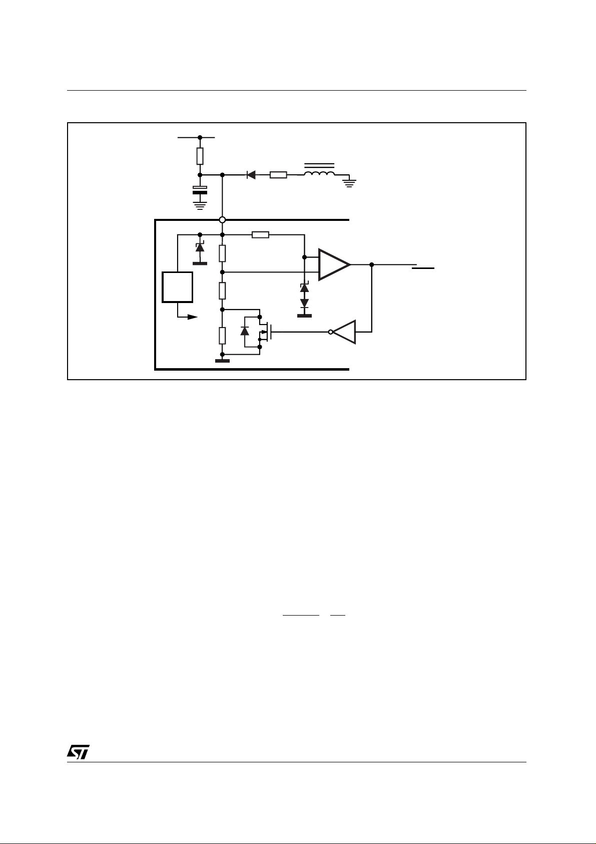
Figure 2. In ter na l Supply Block.
+Vi
REF.
AN966 APPLICATION NOTE
8
-
+
UVLO
D97IN673
ERROR AMPLIFIER AND OVERVOLTAGE DETECTOR BLOCK (see fig. 3 and 4):
The Error Amplifier (E/A) inverting input , through an external divider connected t o the output bus, com-
pares a partition of the boosted output DC voltage, Vo, with the internal reference, so as to maintain the
preregulator output DC voltage constant.
The E/A output is used for frequency compensation, usually realised with a feedback capacitor connected to the inverting input. The E/A bandwidth will be extremely low because the output of the E/A
must be constant over a line half-cycle to achieve high PF.
The dynamics of the E/A output is internally clamped so that it can swing between 2V and 5.8V in order
to speed up the recovery after the E/A saturates low due to an overvoltage or saturates high because of
an overcurrent.
The device is provided with a two-level overvoltage protection (OVP), realized by using the pin connected to the E/A output.
In case of overvoltage, the output of t he E/A will tend to saturate low but t he E/A response is very slow,
so it will take a long time to go into saturation. On the other hand, an overvoltage must be corrected immediately. Hence a fast OVP detector, based on a different concept, is necessary.
In steady state condition, the current through R1 is equal to the current in R2 because the compensation
capacitor does not allow DC current to flow (neither does the high-impedance inverting input of the E/A):
I
R1,R2
=
V
o
R1
=
2.5
R2
− 2.5
When the output voltage rises because of a step load change, the current in R1 builds up as well but the
current through R2, fixed by the internal 2.5V reference, does not because of the E/A slowness. The current in excess will then flow through the feedback capacitor and enter t he low-inpedance E/A output,
where it is sensed. In case, a two-step procedure can occur.
3/21
Page 4
AN966 APPLICATION NOTE
Figure 3. Error Amplifier and Overvoltage Detector Block.
Ccomp.
+Vo
R1
1
-
E/A
R2
D97IN591
2.5V
+
∆I
40µA
When the current in excess reaches about 37µA, the output voltage of the multiplier is forced to decrease thus the energy drawn from the mains is reduced. This slows down the rate of rise of the output
voltage. In some cases, this "soft braking" action is able to prevent the output voltage from exceeding
the regulated value too much.
If the output voltage further increases despite the soft braking, so that the current entering the E/A
reaches 40µA, a "sharp braking" takes place. The output of the multiplier is pulled to ground, thus turning off the output stage and the external MOSFET. Also the internal starter is switched off. The internal
current comparator is provided with hysteresis, t hus the pull-down will be released and the output stage
re-enabled as the current entering the E/A falls approximately below 10µA.
2.25V
∆I
2
X PWM
-
+
DRIVER
Figure 4. Dynamic and Static OVP operation.
V
OUT nominal
40µA
10µA
I
SC
E/A OUTPUT
2.25V
DYNAMIC OVP
STATIC OVP
OVER VOLTAGE
D97IN592A
4/21
Page 5
AN966 APPLICATION NOTE
This dynamic OVP, with its combination of soft and sharp braking, is effective to handle most of load
changes but does not provide a complete protection. In fact it is sensitive to output voltage v ariations
(whence the appellative "dynamic") and cannot reveal a steady overvoltage, which is likely to occur in
case of load disconnection.
The above mentioned concept of the E/A saturation is effective to achieve a "static" OVP. If the overvoltage lasts so long that the output of E/A goes below 2.25V (the E/A is in linear dy namics up to 2.5V), the
protection is activated. Besides turning off the output s tage and t he external MOSFET, it disables some
internal blocks reducing the quiescent current of the chip to 1.4mA (typ). The operation of the device is
re-enabled as the E/A output goes back into its linear region.
Fig. 4 illustrates the combined action of dynamic and static OVP.
ZERO CURRENT DETECTION AND TRIGGERING BLOCK (see fig. 5)
The Zero Current Detection (ZCD) block switches on the external MOSFET as the voltage across the
boost inductor reverses, just after the current through the boost inductor has gone to zero. This feature
allows TM operation.
Figure 5. Zero Current Detection, Triggering and Disable Block.
+Vi
ZCD
5
DISABLE
200µA
-
++
5.7V
-
1.6V0.15V
STARTER
PWM
R
S
Q
DRIVER
D97IN674A
7
GD
As the circuit is running, the signal for ZCD is obtained with an auxiliary winding on the boost inductor.
Of course, a circuit is needed that turns on the external MOSFET at start-up since no signal is coming
from the ZCD. This is r ealized with an internal starter, which f orces the driver to deliver a pulse to the
gate of the MOSFET, producing also the signal for arming the ZCD circuit.
The repetition rate of the starter is greater than 70 µs (≅ 14 kHz) and this maximum frequency must be
taken into account at design time.
DISABLE BLOCK (see fig. 5)
The ZCD pin is used also to act ivate the Disable Block. I f the voltag e on the pin is taken below 150 mV
the device will be shut down. As a result, its current consumption will be reduced. To re-enable the device operation, the pull-down on the pin must be released.
MULTIPLIER BLOCK (see fig. 6)
The multiplier has two inputs: the first one takes a partition of the instantaneous rectified line voltage and
the second one the output of the E/A. If this voltage is constant (over a given line half-cycle) the output
of the multiplier will be shaped as a rectified sinusoid too. This is the reference signal for the current
comparator, which sets the MOSFET peak current cycle by cycle.
5/21
Page 6
AN966 APPLICATION NOTE
Figure 6. Multiplier Block.
Rs
23
E/A
X
4
1.7V
-
CURR.CMP
+
D97IN675
CURRENT COMPARATOR AND PWM LATCH (see fig.7):
The current comparator senses the voltage across the current sense resistor (Rs) and, by comparing it
with the programming signal delivered by the multiplier, determines the exact time when the external
MOSFET is to be switched of f. The P WM latch avoids spurious switchings of the MOSFET which might
result from the noise generated.
The output of the multiplier is internally clamped to 1.7V, (typ.) thus current limiting oc curs if the voltage
across Rs reaches this value.
Figure 7. Current Comparator and PWM latch
Q
R
4
S
X
D97IN676
-
CMP
+
1.7V
R
Q
DRIVER
S
DRIVER (see fig.8)
A totem pole buffer, with 400mA source and sink capability, allows driving an external MOSFET. An in-
ternal pull-down circuit holds the output low when t he device is in UVLO conditions, to ensure that the
external MOSFET cannot be turned on accidentally.
6/21
Page 7
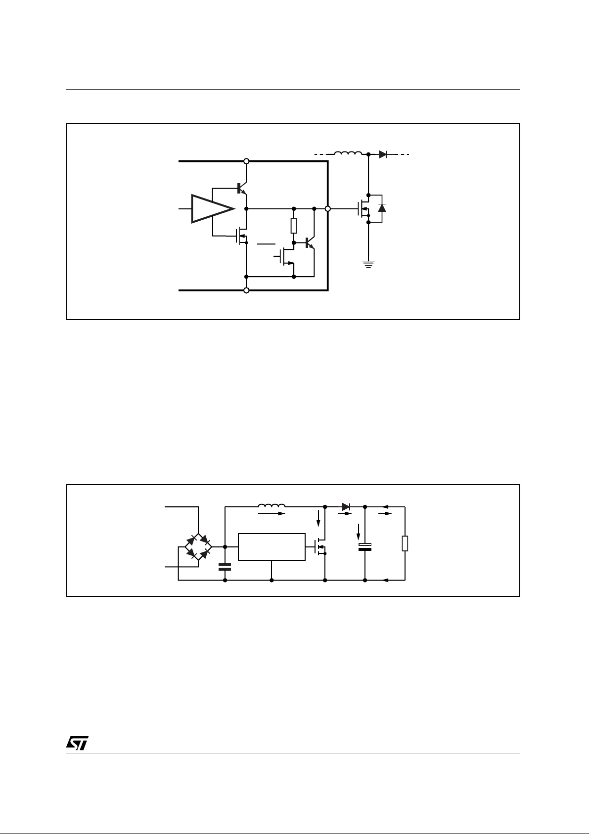
Figure 8. Output Driver.
DRIVER
V
8
6
GND
CC
UVLO
AN966 APPLICATION NOTE
7
GD
D97IN677
Q
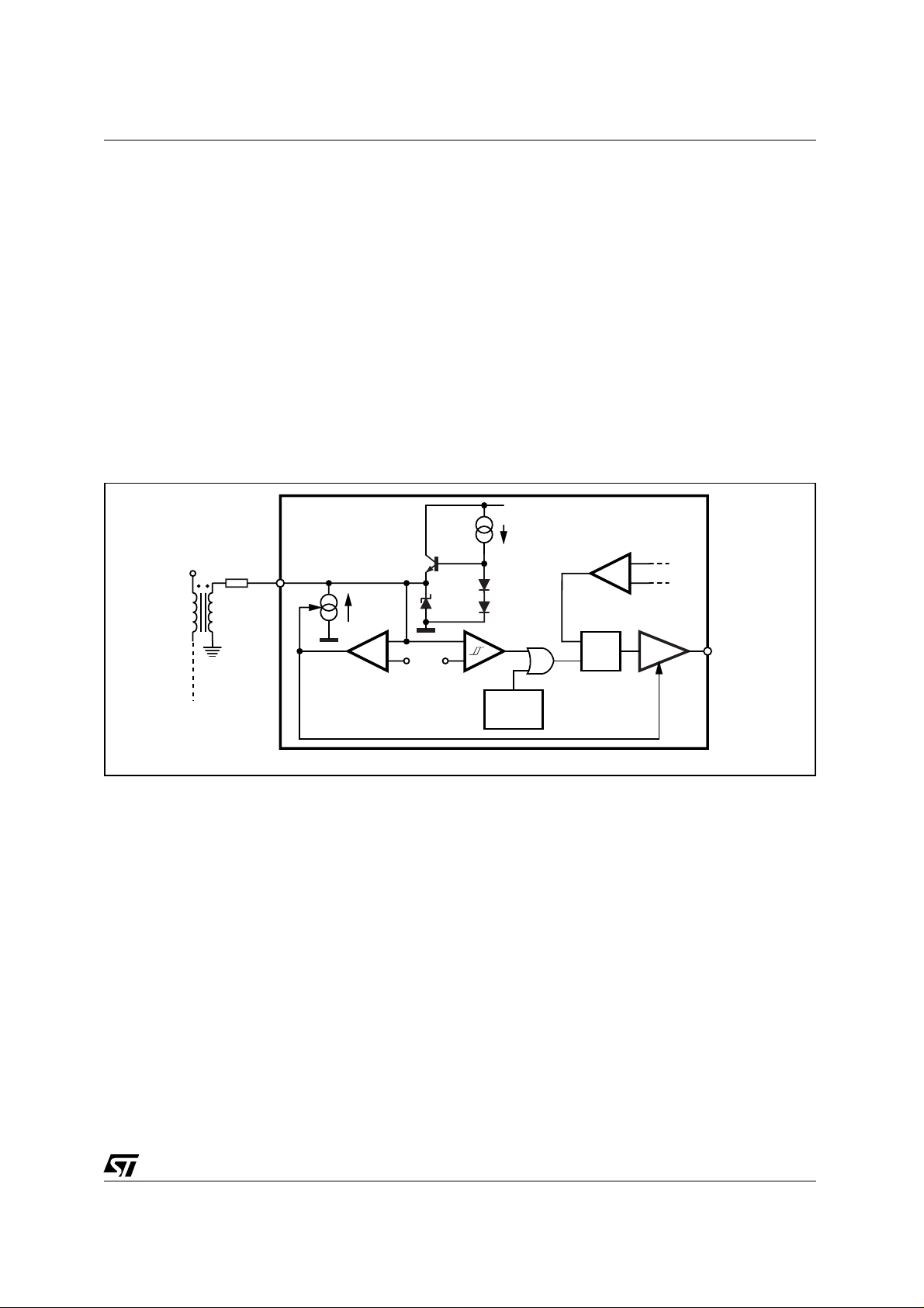
TM PFC Operation
(Boost Topology)
The operation of the PFC Transition Mode controlled boost convert er, can be summarized in the following description.
The AC mains voltage is rectified by a diode bridge and t he rectified voltage delivered to the boost converter. This, using a switching technique, boosts the rectified input v oltage t o a r egulated DC output voltage (Vo).
The boost converter consists of a boost inductor (L), a controlled power switch (Q), a catch diode (D), an
output capacitor (Co) and, obviously, a control circuitry (see fig. 9).
The goal is to shape the input current in a sinusoidal fashion, in-phase with the input sinusoidal voltage.
To do this the L6561 uses the so-called Transition Mode technique.
Figure 9. Boost Converter Circuit.
L
D
~
I
L
~
C
in
I
Q
QCONTROLLER
I
D
I
C
D94IN119
I
O
C
O
LOAD
The error amplifier compares a partit ion of the output voltage of the boost converter with an internal reference, generating a signal er ror propor tional to the difference between them. If the bandwidth of the error amplifier is narrow enough (say, below 20 Hz), the error signal is a DC value over a given half-cycle.
The error signal is fed into the multiplier block and multiplied by a partition of the rectified mains voltage.
The result will be a rectified s inusoid whose peak amplitude depends on the mains peak volt age and the
value of the error signal.
The output of the multiplier is in turn fed into the (+) input of the current comparator, thus it represents a
sinusoidal reference for PWM. In fact, as the voltage on the current sense pin (istantaneous inductor
current times the sense resistor) equals the value on the (+) of the current comparator, the conduction of
the external MOSFET is terminated. As a consequence, the peak inductor current will be enveloped by a
7/21
Page 8

AN966 APPLICATION NOTE
rectified sinusoid. It is possible to prove also that
this operation produces a costant ON-time over
each line half-cycle (see "Boost Inductor").
Figure 10. Inductor Current waveform and
MOSFET tim in g
After the MOSFET has been turned off, the boost
inductor discharges its energy into the load until its
current goes to zero. The boost inductor has now
PEAK
run out of energy, the drain node is floating and the
inductor resonates with the total capacitance of the
drain. The drain voltage drops rapidly below the in-
INDUCTOR CURRENT
stantaneous line voltage and the signal on ZCD
drives the MOSFET on again and another conversion cycle starts.
This low voltage across the external MOSFET at
AVERAGE
turn-on reduces both the switching losses and the
equivalent drain capacitance energy that is dissipated inside the external MOSFET.
The resulting inductor current and the timing intervals of the MOSFET are shown in fig. 10, where it is
also shown that, by geometric relationships, the average input current (the one which will be drawn
from the mains) is just one-half of the peak inductor
MOSFET Q
0
On
Off
D93IN040A
current waveform.
The system operates (not exactly on but very close
to) the boundary between continuous and discontinuous current mode and that is why this system is called a Transition Mode PFC.
Besides the simplicity and the few external parts required, this system minimizes the inductor size due to
the low inductance value needed. On the other hand, the high current ripple on the inductor involves
high RMS current and high noise on the rectified main bus , which needs a heavier EMI filter to be rejected. These drawbacks limit the use of the TM PFC to lower power range applications.
Design Criteria
Here below some design criteria are described. The basic design specification concerns the following
data:
Mains Voltage Range: V
❑
Regulated DC Output Voltage: V
❑
Rated Output Power: P
❑
Minimum Switching Frequency:
❑
Maximum Output Voltage ripple: ∆V
❑
Maximum Overvoltage admitted: ∆V
❑
irms(min)
o
- V
o
ƒ
sw
irms(max)
o
OVP
For reference, it is useful to define also the following quantities:
Expected efficiency: η
❑
Input Power: Pi (= P
❑
Maximum Mains RMS current: I
❑
Rated Output Current: Io (= Po/Vo)
❑
/η)
o
(= Pi/V
rms
irms(min)
)
POWER SECTION DESIGN
Input Bridge
The input diodes bridge can use standard slow recovery, low-cost devices. The quantit ies to consider
will be just the input current (I
), the maximum peak mains voltage and the thermal data of the diodes.
rms
Input Capacitor
The input high frequency filter capacitor (C
) has to attenuate t he switching noise due to the high fre-
in
8/21
Page 9

AN966 APPLICATION NOTE
quency inductor current r ipple (twice the average line current, s ee fig. 9). The worst conditions will occur
on the peak of the minimum rated input voltage.
The maximum high frequency voltage ripple is usually imposed between 1% and 10% of the minimum
rated input voltage. This is expressed by a coefficient r (typically, r = 0.01 to 0.1):
I
ƒ
⋅ r ⋅ V
sw
rms
irms (min
)
= 1/2 ripple peak-to-peak value) is a
O
C(2f)pk
= Io):
=
C
in
2π ⋅
High va lues o f Cin alle viate t he b urden to th e EMI f ilter but ca use t he po wer fac tor and the harmoni c contents of t he mains current to wo r s en, espec ially at high line and light load. On the ot her hand, low value s of
improv e pow er f a ctor and r educ e m ains cur rent dis tort i on but re qu ire h eav ier EMI fil t erin g and incr eas e
C
in
power dissipation in the input bridge. It is up to the designer to find the right trade-off in their application.
Output Capacitor
The output bulk capacitor (C
) selection depends on the DC output voltage, the admitted overvoltage,
o
the output power and the desired voltage ripple.
The 100 to 120Hz (twice the mains frequency) voltage ripple (∆V
function of the capacitor impedance and the peak capacitor current (I
∆
V
O
√
= IO ⋅
2π ⋅ 2f ⋅ C
(
1
)
O
+ ESR
2
2
With a low ESR capacitor the capacitive reactance is dominant, therefore:
I
C
≥
O
O
=
4π ⋅ f ⋅ ∆VO
Vo is usually selected in the range of 1 to 5% of the output voltage.
∆
P
O
4π ⋅ f ⋅ VO ⋅ ∆VO
Although ESR usually does not affect t he output ripple, it has to be taken into ac count for power losses
calculation. The total RMS capacitor ripple current, including mains fr equency and switching frequency
components, is:
I
Crms
=
⋅ I
9
π
2
32
√
√
2
rms
⋅
V
irms
V
2
− I
o
o
If th e application has to guar antee a specifi ed hold-up ti me, the select ion criterio n of the capac itance will
change: Co has to deliver the output power for a certain time (t
⋅ t
2 ⋅ P
C
=
O
V
2
o_min
O
− V
) with a specified maximum dropout voltage:
Hold
Hold
2
op_min
where Vo_min is the minimum output voltage value (which takes load r egulation and output ripple into
account) and Vop_min is the minimum output operating voltage before the ’power fail’ detection from the
downstream system supplied by the PFC.
Boost Inductor
Designing the boost inductor involves several parameters and different approaches can be used.
First, the inductance value must be defined. The inductance (L) is usually determined so that the mini-
mum switching frequency is greater t han the maximum frequency of the inter nal s tarter, to ensure a correct TM operation. Assuming unity PF, it is possible to write:
Ton =
L ⋅ I
√2 ⋅
V
Lpk
irms
⋅ sin
⋅ sin
(θ)
(θ)
=
L ⋅ I
√2 ⋅
V
Lpk
irms
Toff =
Vo −
L ⋅ I
√2 ⋅
Lpk
⋅ sin
V
irms
(θ)
⋅ sin
(θ)
9/21
Page 10

AN966 APPLICATION NOTE
being Ton and Toff the ON-time and the OFF-time of the power MOSFET respectively, I
the maxi-
Lpk
mum peak inductor current in a line cycle and θ the instantaneous line phase (θ∈(0, π)). Note that the
ON-time is constant over a line cycle.
As previously said, I
is twice the line-frequency peak current, which is related to the input power and
Lpk
the line voltage:
P
I
Lpk
= 2 ⋅
√2 ⋅
i
.
V
irms
Substituting this relationship in the expressions of Ton and Toff, af ter some algebra it is possible to f ind
the instantaneous switching frequency along a line cycle:
2
⋅ (VO −
f
(θ) =
sw
1
Ton + Toff
=
2 ⋅ L ⋅ P
1
V
irms
⋅
i
√2 ⋅
V
O
V
irms
⋅ sin
(θ))
.
The switching frequency will be minimum at the top of the sinusoid (θ = π/2 ⇒ sin(θ) =1 ), max imum at
the zero crossings of the line voltage (θ = 0 or π ⇒ sin(θ) = 0) where Toff = 0.
The absolute minimum frequency
ƒ
can occur at either the maximum or the minimum mains volt-
sw(min)
age, thus the inductor value is defined by:
2
where V
can be either V
irms
irms(min)
The minimum suggested value for
L =
or V
ƒ
sw(min)
⋅ (VO −
V
irms
2 ⋅
ƒ
sw (min
irms(max)
, whichever gives the lower value for L.
is 15 kHz, not to interfere with the internal starter (see ZCD
√2 ⋅
⋅ Pi ⋅ V
)
V
irms
O
)
,
and triggering block description) .
Once defined the value of L, the real design of the inductor can start. As to the magnetic material and
the geometry, the need of isolation due t o the high voltage, and the operating frequency range make the
standard high frequency ferrite (gapped core-set with bobbin) the usual choice in PFC applications.
Among the various types offered by manufacturers the most suitable one will be selected with technical
and economic considerations.
The next step is to estimate the core size. To get the approximated value of the minimum core size, it is
possible to use the following practical formula:
2
l
gap
,
rms
l
e
.
where Volume is expressed in cm
the gap length (l
The ratio l
e/lgap
) and the effective magnetic length (le) of the ferrite core:
gap
is fixed by the designer.
Volume ≥ 4K ⋅ L ⋅ I
3
, L in mH and the specific energy constant K depends on the ratio of
3
K ≅ 14 ⋅ 10
−
⋅
Then the winding must be specified. The turn number an d the wire c ross-section are the quant ities t o be
defined.
The (maximum) instantaneous energy inside the boost inductor (1/2 ⋅ L ⋅ I
2
) can be expressed in
Lpk
terms of energy stored in the magnetic f ield, given by the maximum energy density times the effective
core volume V
:
e
2
1
⋅ L ⋅ I
2
Lpk
1
=
⋅ ∆H ⋅ ∆B ⋅ Ve ≈
2
1
⋅ ∆H ⋅ ∆B ⋅ Ae ⋅ Ie,
2
where: A
is the effective ar ea of the core cross-section, ∆H is the swing of the magnetic field strength
e
and ∆B is the swing of the magnetic flux density.
To prevent the core from saturating because of its high permeability and allow an adequate ∆H, it is nec-
essary to introduce an air gap.
Despite the gap length l
is few per cent of le, the permeability of ferrite is so high (for power f errites,
gap
typically µr = 2500) that it is pos s ible to assume all the m agnetic field concentrated in the air gap with g ood
approximation (∆H ≈ ∆H
). For instance, with 1% of l
gap
ror caused by this assum ptio n i s a bo u t 4%. The error will b e s m alle r i f th e l
10/21
(which is the minimum s uggested value) the er-
gap/le
ratio is large r .
gap/le
Page 11

AN966 APPLICATION NOTE
As a result, neglecting fringing flux in the air gap region, the energy balance can be re-written as:
2
L ⋅ I
≈ ∆H
Lpk
The flux density ∆B is the same throughout the core and the air gap and is related to the field strength
inside the air gap by the well-known relationship:
⋅ ∆B ⋅ Ae ⋅ I
gap
gap
∆B = µ
⋅ ∆H
0
gap
.
Then, considering Ampere’s law (applied to the air gap region only):
I
gap
⋅ ∆H
gap
≈ N ⋅ I
Lpk
,
from the energy balance equation it is possible to obtain:
2
⋅ A
N
L ≈
I
gap
e
⇒ N ≈
⋅
µ
0
L ⋅ l
√
⋅ A
µ
ο
gap
,
e
where N is the turn number of the winding.
As N is defined, it is recommended to check for the saturation of the core (see Pin 4 description). If the
check shows a result too close to the rated limit, an increase of l
and a new calculation will be neces-
gap
sary.
The wire gauge selection is based on limiting the copper losses at an acceptable value:
2
4
P
=
⋅ I
CU
due to the high frequency ripple the effective wire resistance R
⋅ RCU;
rms
3
is increased by skin and proximity ef-
CU
fects. For this reason Litz wire or multi-wire solutions are recommended.
Finally, the space occupied by the winding will be evaluated and, if it does not fit the winding area of the
bobbin, a bigger core set will be considered and the winding calculation repeated.
It is now necessary to add an auxiliary winding to the inductor, in order for the ZCD pin to recognize
when the current through the inductor has gone to zero. It is anyway a low cost thin wire winding and the
turns number is the only parameter to be defined (see Pin 5 description).
POWER MO SFET
The choice of the MOSFET concerns mainly its R
, which depends on the output power, since the
DSon
breakdown voltage is fixed just by the output voltage, plus the overvoltage admitted and a safety margin.
The MOSFET’s power dissipation depends on conduction and switching losses.
The conduction losses are given by:
ON
= I
2
Qrms
⋅ R
DSon
P
where:
I
Qrms
= 2 ⋅
√2 ⋅
rms
6
1
√
I
⋅
−
9
irms
⋅
π
.
V
O
2
4
V
√
The switching losses due to current-voltage cross occur only at turn-off because of the TM operation:
P
CROSS
= VO ⋅ I
rms
⋅ t
fall
⋅
,
ƒ
sw
11/21
Page 12

AN966 APPLICATION NOTE
where t
is the crossover time at turn-off. At turn-on the loss is due to the discharge of the total drain
fall
capacitance inside the MOSFET itself. In general, these losses are given by:
P
=
CAP
where C
is the internal drain capacitance of the MOSFET (@ VDS = 25V), Cd is the total external
oss
drain parasitic capacitance and V
3.3 ⋅ C
oss
⋅ V
1.5
DRAIN
is the drain voltage at MOSFET turn-on. In practice it is possible
DRAIN
+
1
⋅ Cd ⋅ V
2
to give only a rough estimate of the total switching losses because both
given line half-cycle. V
, in particular, is affected not only by the sinusoidal change of the input volt-
DRAIN
2
DRAIN
,
⋅
ƒ
sw
ƒ
sw
and V
change along a
DRAIN
age but also by the drop due to the resonance of t he boos t inductor with the total drain capacitance (see
fig. 12). This causes, at low mains voltage, V
to be zero during a significant portion of each line
DRAIN
half-cycle. It is possible to show that "Zero-Voltage-Switching" occurs as long as the instantaneous line
voltage is less than half the output voltage.
BOOST DIODE
The boost freewheeling diode will be a f ast recovery one. The value of it s DC and RMS current, useful
for losses computation, are respectively:
I
= I
Do
o
2
4
V
√
I
Drms
= 2 ⋅
√2 ⋅
I
⋅
rms
√
9
irms
⋅
π
.
V
O
The conduction losses can be estimated as follows:
2
Drms
,
where V
P
= Vto ⋅ IDo + Rd ⋅ I
DON
(threshold voltage) and Rd (differential resistance) are parameters of the diode.
to
The breakdown voltage is fixed with the same criterion as the MOSFET.
L6561 Biasing Circuitry (pin by pin)
Please, refer to the schematic circuit shown in fig. 13.
(INV) leads both to the inverting input of the E/A and to the OVP circuit. A resistive divider will be
Pin 1
connected between the regulated output voltage of the boost and the pin.
The internal reference on the non-inverting input of the E/A is 2.5V and the OVP alarm level current is
40µA. R11+ R12 and R13 will be then selected as follow:
R11 + R12
R13
(COMP) is the output of the E/A and also one of the two input s of the multiplier. A feedback com-
Pin 2
=
V
O
− 1 R11 + R12 =
2.5V
V
∆
40 µA
OVP
,
pensation network, placed between this pin and INV (1), reduces the bandwidt h so to avoid the attempt
of the system to control the output voltage ripple (100-120Hz).
In the sim plest case, this com pensation is just a capacitor, which provides a low frequenc y pole as well as a
high DC gain. A simple criterion to define the capacitance value, is to to provide ~60dB attenuation at
100Hz:
C23 =
10
2 π ⋅ R7
Please refer to [1] for more information on how to compensate the E/A.
12/21
Page 13

(MULT) is the second multiplier input . It will
Pin 3
be connected, through a resistive divider, to the rectified mains to get a sinusoidal voltage reference.
The multiplier can be described by the relationship:
= k ⋅ ( V
V
cs
− 2.5V ) ⋅ V
COMP
MULT
where VCS (Multiplier output) is the reference for the
current sense, k is the multiplier gain, V
voltage on pin 2 (E/A output) and V
MULT
is the
COMP
is the volt-
age on pin 3.
A complete description is given by the diagram of
fig. 11, which shows the typical multiplier characteristics family. The linear operation of the multiplier
is guaranteed inside the range 0 to 3V of V
the range 0 to 1.6V of V
, while the minimum
CS
MULT
and
guaranteed value of the maximum slope of the
characteristics family (∆V
CS
/∆V
) is 1.65. Taking
MULT
this into account, the following is the suggested procedure to set properly the operating point of the
multiplier.
AN966 APPLICATION NOTE
Figure 11. Multiplier characteristics family
V
(pin4)
V
CS
upper voltage
(V)
clamp
1.6
1.4
1.2
1.0
0.8
0.6
0.4
0.2
0
0 0.5 1.0 1.5 2.0 2.5 3.0 3.5 4.0 4.5
5.0
4.5
4.0
V
MULT
D97IN555A
(pin3) (V)
COMP
3.5
3.2
3.0
2.8
2.6
(pin2)
(V)
First, the maximum peak value for V
MULT
, V
MULTpkx
, is selected. This value, which will occur at maximum
mains voltage, should be 3V or nearly so in wide range mains and less in case of single mains. The
minimum peak value, occurring at minimum mains voltage will be:
V
irms(min
V
MULTpkmin
= V
This value, multiplied by the minimum guaranteed
the multiplier:
V
= 1.65 ⋅ V
XCSpk
If the resulting V
peated beginning with a lower V
exceeds the linearity limit of the current sense (1.6V), the calculation should be re-
XCSpk
MULTpkx
value.
MULTpkx
V
∆
CS
V
∆
MULT
⋅
V
will give the maximum peak output v oltage of
MULTpkmin
irms(max
)
)
In this way, the divider will be such that:
R3
R1 + R2 + R3
=
√2 ⋅
V
MULTpkx
V
irms(max
)
the individual values can be chosen by setting the current through R3, in the hundreds µA or less to minimise power dissipation.
(CS) is t he inv ert ing i npu t of the c urre nt s ense compar at or. Th rou gh this pin , the L6 561 read s the in -
Pin 4
stantan eou s indu ct or curr en t, con vert ed to a propor ti ona l volta ge by an ex tern al sens e resist or (Rs). As this
signal cr os ses t he t hresh old set by the mu lt iplie r out put, th e PWM la t ch is re set an d the p ower MOSFET is
turned off. The MOSFET will stay in OFF-state until the PWM latch is set again by the ZCD signal. An internal circuit ensures that the PWM latch cannot be set until the signal on pin 4 has disappeared.
The sense resistor value is calculated as follows:
where V
≤
R
S
has been calculated as per described earlier and:
XCSpk
I
= 2
Rspk
V
XCSpk
I
Rspk
√2 ⋅
I
,
rms
13/21
Page 14

AN966 APPLICATION NOTE
The power dissipated in Rs, is given by:
P
= Rs ⋅ I
Rs
The internal 1.8V (max.) zener clamp on t he non-inverting input of the PWM comparator sets a current
limitation threshold, so that the maximum current through Rs can be as high as:
2
Qrms
.
I
Rspkmax
=
1.8
R
.
s
This will be the maximum inductor current as well, therefore one must make sure that the boost inductor
does not saturate at this current level, which is very likely to be reached when the boost converter is
powered on (especially at low line) or powered off.
Pin 5 (ZCD) is the input to the Zero Current Detector circuit. The ZCD pin will be connected to the
Pin 5
auxiliary winding of the boost inductor through a limiting resistor.
The ZCD circuit is negative-going edge-triggered: when the voltage on the pin falls below 1.6 V the
PWM latch is set and the MOSFET is turned on. To do so, however, the circuit must be armed first: prior
to falling below 1.6V the voltage on pin 5 must experience a positive-going edge exceeding 2.1 V (due to
MOSFET ’s turn-off).
The maximum main-to-auxiliary winding turn ratio, m, has to ensure that the voltage delivered to the pin
during MOSFET’s OFF-time is sufficient to arm the ZCD circuit. Then:
−
m ≤
V
o
√2 ⋅
V
irms (max.
2.1
)
If the winding is used als o for supplying t he IC, the above criterion may not be compatible with the Vcc
voltage range. To solve this incom patibilit y the self-supply network shown in the schematic of fig. 13 can
be used. The minimum value of the limiting resistor can be found assuming 3 mA current through the pin
and considering the maximum voltage (the absolute value) across the auxiliary winding.
The actual value can be then fine-tuned trying to make the turn-on of the MOSFET occur exactly on the
valley of the drain voltage oscillation (the boost inductor, completely discharged, is ringing with the drain
Figure 12. Optimum MOSFET Turn-on
capacitance, see fig. 12). This will minimize the
power dissipation at turn-on.
If the pin is driven by an external signal, the
V
DRAIN
L6561 will be synchronized to (the negative-going edges of) that signal. If left floating, the
V
O
L6561 will work at the frequency of its internal
starter. Obviously, neither TM operation will take
place nor high P F will be ac hieved in this case,
V
ipk
but these characteristics can be exploited in applications other than PFC.
This pin incorporates also a disable function.
The device will be shut down if the voltage on
the pin is forced externally below 150mV. To do
so, up to 10mA must be sunk from the pin. The
quiescent current of the IC will be reduced at
t
V
ZCD
5.7
about 1.4 mA. The device will restart as the external pull-down is removed since an internal
150µA generator pulls up the pin.
14/21
2.1
1.6
0.7
D97IN678A
(GND). This pin acts as t he current r eturn
Pin 6
both for the signal i nternal circuitry and for the
gate drive current. When layouting the printed
circuit board, these two paths should run separately.
t
Page 15

AN966 APPLICATION NOTE
(GD) is the output of the driver. The pin is able to drive an external MOSFET with 400mA source
Pin 7
and sink capability.
To avoid undesired switch-on of the external MOSFET because of some leakage current when the sup-
ply of the chip is below the UVLO threshold, an internal pull-down circuit holds the pin low. The circuit
guarantees 0.3V maximum on the pin (@ I
resistor connected between the gate and the source of the external MOSFET used to this purpose.
Pin 8
cc
) is the supply of the device. Thi s pin will be externally connected to the start-up circuit (usu-
(V
ally, one resistor connected to the rectified mains) and to the self-supply circuit.
Whatever the configuration of the self-supply system, a capacitor will be connected between this pin and
ground.
To start the L6561, the voltage must exceed the start-up t hreshold (13V max.). Below this value the de-
vice does not work and consumes less than 90µA from V
sistors (in the hundreds kΩ), which reduces power consumption and optimises system efficiency at low
load, especially in wide range mains applications.
When operating, the current consumption (of the device only, not considering the gate drive current)
rises to a value depending on the operating conditions but never exceeding 4.5mA.
The device keeps on working as long as the supply voltage is over the UVLO threshold (10.3V max).
If the Vcc voltage exceeds 18V an internal zener diode, 30 mA rated, will be activated that clamps the
voltage. In that case t he power consumption of the device will increase considerably, but there is no
harm as long as the current is below the maximum rating.
= 10mA), with Vcc > 3V. This allows omitting the "bleeder"
sink
. This allows the use of high value start-up re-
cc
PRACTICAL DESIGN EXAMPLE
To fix the main concepts, here below the wide range demonstration board design is described and the
results of the board evaluation are presented.
The target specifications are summarised in table1. To meet them an appropriate selection, especially
as to critical components, is an important step.
Table 1. Wide Range PFC Target Specification.
AC mains RMS voltage V
DC output regulated voltage V
Rated output power Po = 80W
Minimum switching frequency f
Expected efficiency
Full load output voltage ripple
Maximum output overvoltage
= 85 to 265V
irms
= 400V
o
= 35kHz
sw(min)
> 90%
η
V
∆
≤ ±
o
= 60V
V
∆
OVP
10V
POWER MO SFET:
Two parameters are useful to select the suitable device: the minimum blocking voltage V
R
because of power dissipation.
DSON
The device selected is the S TP8NM50 (MDMESH) (V
(BR)DSS
= 500V, R
= 0.8Ω @ 25°C, 1.6Ω @
DSON
(BR)DSS
and the
125°C). The estimated power dissipation is 1.6W total. A 40°C/W heat sink is provided to keep die temperature at a safe value.
BOOST DIODE (D1):
The plastic axial diode STTH1L06 (Turbo2, 1A 600V) has been selected. The power dissipation is esti-
mated about 0.24W.
BOOST INDUCTOR (T):
The inductance value (L) is as high as 0.7 mH, which leads to a minimum switching frequency of 35kHz.
15/21
Page 16

AN966 APPLICATION NOTE
Assuming an l
Considering the E series, the E25 (2.99 cm
ratio of 2.5% t he minimum core size estimate gives a minimum volume of 2.6 cm3.
gap/le
3
effective volume) has been selected.
To reduce copper losses, a multiple wir e ( 20 x 0.1mm) has been adopted. The resistance of the winding
is about 0.75Ω at 35 kHz , so the maximum copper losses are about 1W.
OUTPUT FILTER CAPACITOR (C6):
The specification on the output voltage ripple determines the capacitance value.
Assuming 50 Hz minimum line frequency, a 47µF/450V capacitor has been selected. This gives an out-
put ripple ∆Vo = ±7 V.
MULTIPLIER SETTING (R1, R2, R3) AND SENSE RESISTOR (R9, R10):
The multiplier divider is selected so to exploit about 80% of its linear dynamics (V
MULTpkx
= 2.5V) as per
the procedure described in pin 3 description. The sense resistor is then determined.
As to R9 and R10, metal film resistors are suitable because of the high peak current flowing in it.
OUTPUT DIVIDER (R11, R12, R13):
R11 + R12 is selected so to achieve the desired overvoltage t rip level (∆V
= 60V), while R13 is cho-
OVP
sen so to get the specified output regulated voltage.
ERROR AMPLIFIER COMPENSATION
The error amplifier has been compensated so as to get a type 2 amplifier that provides a pole at the ori-
gin and a zero-pole pair. As compared to a type1 amplifier (compensated with a single capacitor) this
compensation offers a higher phase margin under all operating conditions and is therefore recommended when the PFC pre-regulator powers a DC-DC converter. However, the twice-mains-frequency
gain will be higher because of the zero, which causes a higher ripple at the output of the E/A and, as a
result, a higher 3rd harmonic (and a higher THD) of the current drawn from the mains.
THD REDUCER
In the PCB there is provision f or a network (see schematic of figure 13, in the dotted box) able to reduce
the crossover distortion of the PFC input current, that is the small flat region appearing at the zero crossings of the mains voltage. The effect of this circuit is to force the ON-time of the power switch to increase
nearby the zero-crossings. As a result, the energy inside the boost inductor will be greater and the deadtime during which there is no energy transfer is reduced. The circuit fine-tuning has to be made experimentally.
NTC
The NTC has been moved from the input to the output, in series with the boost diode. In this way,
though still doing its job of inrush current limiter, it will undergo the output current instead of the input
current, as in the typical position, with a considerable power dissipation reduction. The extra voltage on
mosfet’s drain while the boost diode is conducting is negligible.
The schematic circuit of fig. 13 shows the values of all the parts used. In fig. 14 the printed circuit board
and the component layout of the demonstration board are shown.
16/21
Page 17

AN966 APPLICATION NOTE
Figure 13. 80W, Wide Range Demonstration Board(EVAL6561-80): Electrical Circuit
NTC
D1
2.5
Ω
R11
750 k
R12
750 k
R13
Ω
9.53 kΩ
R4
R5
180 k
C29
22 µF
25V
Ω
D8
1N4150
D2
1N5248B
4A/250V
Vac
(85V to 265V)
FUSE
Ω
180 k
R1
Ω
750 k
BRIDGE
C1
W04M
+
-
Boost Inductor Spec (ITACOIL E2543/E)
1 µF
400V
R2
Ω
750 k
C2
10nF
R3
10 k
Ω
E25x13x7 core, 3C85 ferrite
1.5 mm gap for 0.7 mH primary induc tance
Primary: 105 turns 20x0.1 mm
Second ary: 11 turns 0.1mm
Table 2. EVAL6561-80 Evaluation Results
C5 12 nF
C4
100 nF
R14
Ω
100
R6
68 k
Ω
5
8
3
6
D3 1N4148
C7
10 µF
35 V
T
R50 12 k
C3 470 nF
C23
1 µF
21
91 k
R16
7
4
R15
Ω
220
L6561
THD REDUCER (optional)
STTH1L06
Ω
R7
Ω
33
Ω
0.41
R9
1W
Ω
MOS
STP8NM50
R10
0.41
1W
Vo=400V
Ω
Ω
Po=80W
C6
47 µF
450V
-
Vin (Vac) Pin (W) Vo (Vdc)∆Vo (Vdc) Po (W)
η
(%)
w/o THD reducer with THD reducer
PF THD (%) PF THD (%)
85 87.2 400.1 14 80.7 92.8 0.999 3.7 0.999 2.9
110 85.2 400.1 14 80.7 94.7 0.996 5.0 0.996 3.2
135 84.2 400.1 14 80.7 95.8 0.989 6.2 0.989 3.7
175 83.5 400.1 14 80.7 96.6 0.976 8.3 0.976 4.3
220 83.1 400.1 14 80.7 97.1 0.940 10.7 0.941 5.6
265 82.9 400.1 14 80.7 97.3 0.890 13.7 0.893 8.1
Figure 14. EVAL6561-80: PCB and Component Layout (Top view, real size 57x108mm)
17/21
Page 18

AN966 APPLICATION NOTE
DEMO BOARD EVALUATION RESULTS
To evaluate the performance of the PFC demonstration board, the following parameters have been
measured: PF(Power Factor), THD%(Current Total Harmonic Distortion), ∆Vo (Peak-to-Peak Output
Voltage Ripple), Vo (Output Voltage), η (Efficiency).
The test equipment set-up is shown in fig. 15 and the results are shown in table 2.
The harmonic content measurement has been done with an EMI/RFI filter interposed between the AC
source and the demo board under test, while the efficiency has been calculated without the filter contribution. The filter is configured as shown in fig. 16, where:
T1 = 2 x 15mH, T2 = 2 x 47mH, Cx
Figure 15. Test Equipment Set-up
= 0.47µF / 630V, Cx2 = 0.68µF/630V
1
AC POWER
SOURCE/ANALYZER
HP6813A
Figure 16. EMI Filter Configuration
T1 T2
LINE
EMI FILTER
C
x1
L6561
PFC DEMO
C
x2
RESISTIVE
LOAD
D97IN679
PFC
D97IN680
18/21
Page 19

AN966 APPLICATION NOTE
APPLICATION IDEAS
The L6561 is a versatile device. Besides the typical application as a PFC preregulator based on boost
topology, it fits also other applications and/or topologies. Some application hints are given in the following.
Figure 17. Wide Range 50W PFC, Flyback Topology.
2A fuse
85 to 265
Vac
680 nF
1.5 M
1.5 M
Ω
Ω
220 k
220 k
Ω
P6KE160P
Ω
1N4937
BYW80-150
2200 µF
25V
1N4148
220 pF
20 k
22 µF
39 k
3
1 µF
2
Ω
4N35
100 k
2.4 k
L6561
1
6
Ω
Ω
8
5
Ω
10
7
4
0.33
1/2 W
Ω
STP7NA60
Ω
4.7 nF
Tran sformer spec:
Core: ETD29, 3C85 grade
Pri: 2 paralleled windings, 71 T/AWG27 each
Sec: 17 T, 5xAWG27 sandwiched
Aux: 10T, AWG32 evenly spaced
lgap: 1mm for 620 µH primary i nductance
Figure 18. Power Factor Corrected Lamp Ballast using the L6569 driver.
176 to 265
Vac
FUSE
Bridge
R9 220K 1W
D1 BYT11600
C3 680nF
R1
750K
R3
68K
2
C1
220nF
400V
R1A
5
750K
L6561
3
C2
R2
10nF
8.2K
NTC
100
T1
R8
9.53K
22µF
450V
10µF
D3 1N4148
DZ1 4.7V
C5
D2
1N4148
R11
C6
P0102AA
SCR
10µF
22
C8
R7
750K
STP5NA50
Q1
1
R4 10
7
R29
R7A
.6K
8
6
4
750K
R6
1
DZ2
18V
R12
2.2M
D4 1N4148
C9
100nF
C10
470nF
R13 47
820pF 600V
C11 100nF
8
1
L6569
4
23
16K
R14
DZ3 5.6V
R31
1.5M
C12
7
6
5
C13
470pF
Q4
S170
STP6NB50
R15 10
R17
10K
STP6NB50
R16 10
R18
10K
C14
560pF
Q2
Q3
180K
2200 µF
25V
R20
330K
C15
100nF
250V
24 Vdc / 2A
3.3 k
Ω
20 kΩ22 k
Ω
4N35
47 k
Ω
1 nF
TL431
R19
2.3mH
2.3mH
C15A
100nF
250V
4.7 k
Ω
C16
LP1
L1
L2
LP2
6.8nF
630V
6.8nF
630V
R21
R23
820K
820K
R24
R22
C17
1.5M
1.5M
R10
DZ4
56K
20V
D97IN682
R26
2.2M
R28
56K
R30
2.2M
D5
1N4148
R25
C18
82K
1µF
R27
220
19/21
Page 20

AN966 APPLICATION NOTE
Figure 19. Vmains=277 Vac, Vo=320V, Po=140W buck-boost topology
FUSE
Vac
277V +10%
-15%
BRIDGE
4 x BY255
+
-
C1
0.22µF
630V
R9
1.8M
5%
R10
6.2K
5%
C6
10nF
V
CC
R1
68K 5%
C2
22µF
25V
T
C3 330nF
5
8
21
L6561
3
6
C4
1nF
STP5N80
R5 10
7
4
R4 330
R6 0.47
D1 BYT13-800
MOS
1W
82µF/100µF
R11 62K 1%
R12
330K
C5
385V
LM358
R3 12K 1%
-
Vo=320V
Po=140W
+
R7
V
R2
CC
A
8
+
3
2
4
1.3M
1%
1.3M
1%
R8
12K
1%
TRANSFORMER
T: core THOMSON-CSF B1ET2910A
primary 150T of Litz wire 10 x 0.2mm
secondary 7T of #32 AWG (0.15mm)
primary inductance: 3mH
REFERENCE:
[1] "Control loop modelling of L6561-based TM PFC" (AN1089).
D97IN681
20/21
Page 21

AN966 APPLICATION NOTE
Information furnished is believ ed to be accura te an d rel i abl e. However, STM i croelectronics ass um es no responsibil ity for the consequences
of use of such informati on nor for any infringement of patents or other ri ghts of third parties which may result from its use. No license is
granted by implication or otherw ise under any patent or patent rights of STMic roelectronics . Specification mentioned in this publication are
subject to c hange without notice. T hi s publication supersedes and replac es all information previously su ppl ie d. S TMicroelectronics products
are not authorized for use as critical components in life support devices or systems without express written approval of STMicroelectronics.
The ST logo is a registered trademark of STMicroelect roni cs
© 2003 STMicroelectronics – Printed in Italy – All Rights Reserved
STMicroelectronics GROUP OF COMPANIES
Australia-Brazil-Canada-China-Finland-France-Germany- Hong Kong-India-Israel-Italy-Japan-Malaysia-Malta-Morocco-Singapore- Spain-
Sweden-Switzerland-United Kingdom-United States.
http://www.st.com
21/21
 Loading...