

AN937
Application Note
Designing with L4971, 1.5 A high efficiency DC-DC converter
Introduction
The L4971 is a 1.5 A monolithic dc-dc converter, step- down, operating at fix frequency
continuous mode. It is designed in BCD60 II technology, and it is available in two plastic
packages, DIP8 and SO16L.
One direct fixed output voltage at 3.3 V ±1% is available, adjustable for higher output voltage
values, till 40 V, by an external voltage divider.
The operating input supply voltage ranges from 8 V to 55 V, while the absolute value, with no
load, is 60V. New internal design solutions and superior technology performance allow to
generate a device with improved efficiency in all the operating conditions and with reduced
EMI due to an innovative internal driving circuit, and reduced external component counts.
While internal limiting current and thermal shutdown are today considered standard
protection functions, mandatory for a safe load supply, oscillator with voltage feed forward
improves line regulation and overall control loop.
Soft-start avoids output over voltage at turn-on, while, shorting this pin to ground, the device
is completely disabled, going into zero consumption state.
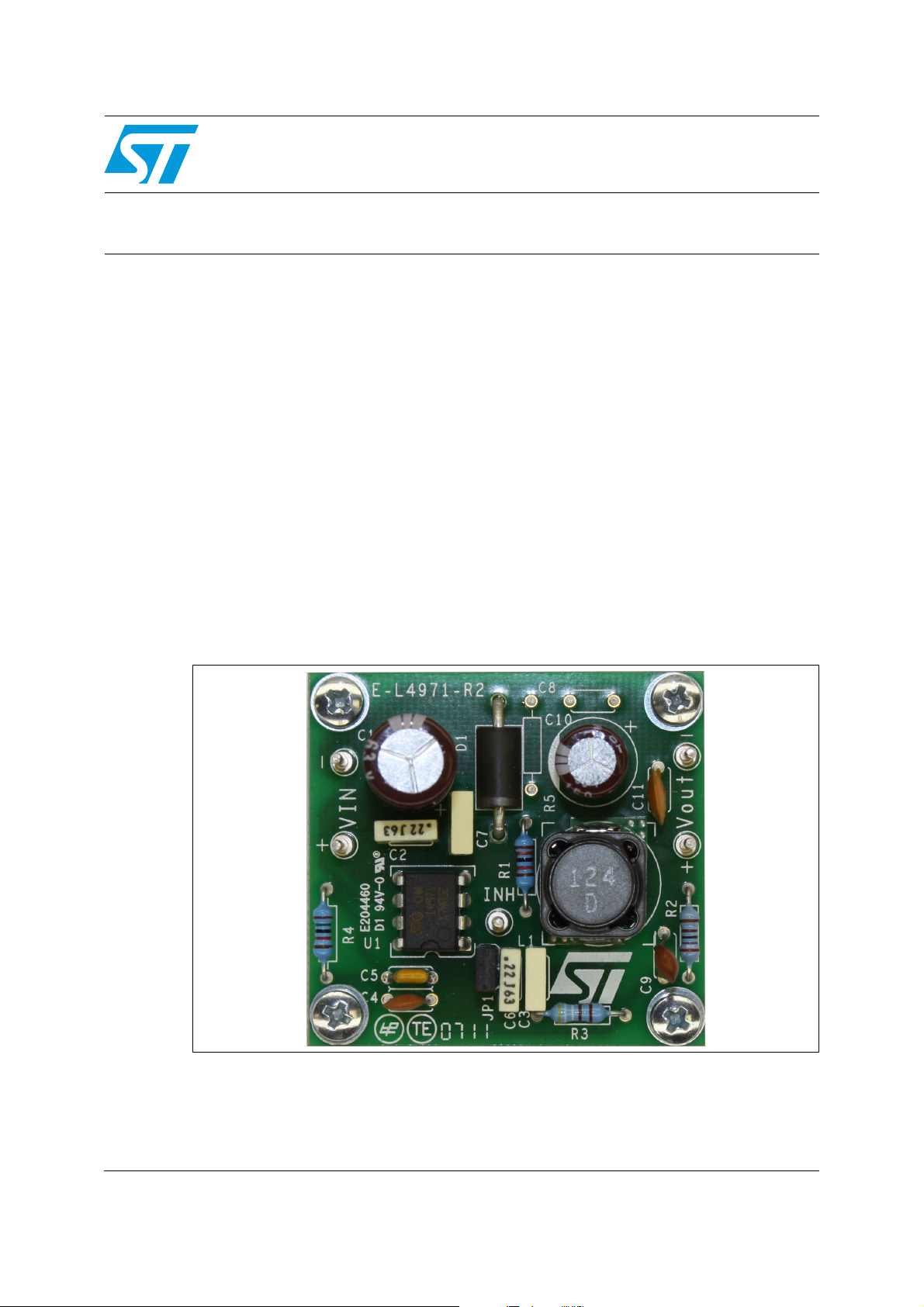
Figure 1. Demonstration board
May 2011 Doc ID 5655 Rev 15 1/29
www.st.com

Contents AN937
Contents
1 Device description . . . . . . . . . . . . . . . . . . . . . . . . . . . . . . . . . . . . . . . . . . 3
2 Power supply, UVLO and voltage reference . . . . . . . . . . . . . . . . . . . . . . 4
2.1 Oscillator and voltage feed forward . . . . . . . . . . . . . . . . . . . . . . . . . . . . . . 4
2.2 Current protection . . . . . . . . . . . . . . . . . . . . . . . . . . . . . . . . . . . . . . . . . . . . 6
2.3 Soft-start and inhibit functions . . . . . . . . . . . . . . . . . . . . . . . . . . . . . . . . . 10
2.4 Feedback disconnection . . . . . . . . . . . . . . . . . . . . . . . . . . . . . . . . . . . . . . 14
2.5 Zero load . . . . . . . . . . . . . . . . . . . . . . . . . . . . . . . . . . . . . . . . . . . . . . . . . 14
2.6 Output overvoltage protection (OVP) . . . . . . . . . . . . . . . . . . . . . . . . . . . . 14
2.7 Power stage . . . . . . . . . . . . . . . . . . . . . . . . . . . . . . . . . . . . . . . . . . . . . . . 15
2.8 Turn - on . . . . . . . . . . . . . . . . . . . . . . . . . . . . . . . . . . . . . . . . . . . . . . . . . . 15
2.9 Turn - off . . . . . . . . . . . . . . . . . . . . . . . . . . . . . . . . . . . . . . . . . . . . . . . . . . 16
3 Typical application . . . . . . . . . . . . . . . . . . . . . . . . . . . . . . . . . . . . . . . . . 17
3.1 Electrical specification . . . . . . . . . . . . . . . . . . . . . . . . . . . . . . . . . . . . . . . 17
3.2 Input capacitor . . . . . . . . . . . . . . . . . . . . . . . . . . . . . . . . . . . . . . . . . . . . . 17
3.3 Output voltage selection . . . . . . . . . . . . . . . . . . . . . . . . . . . . . . . . . . . . . . 19
3.4 Inductor selection . . . . . . . . . . . . . . . . . . . . . . . . . . . . . . . . . . . . . . . . . . . 19
3.5 Output capacitors . . . . . . . . . . . . . . . . . . . . . . . . . . . . . . . . . . . . . . . . . . . 21
3.6 Compensation network . . . . . . . . . . . . . . . . . . . . . . . . . . . . . . . . . . . . . . 22
3.7 Error amplifier and compensation blocks . . . . . . . . . . . . . . . . . . . . . . . . . 23
3.8 LC filter . . . . . . . . . . . . . . . . . . . . . . . . . . . . . . . . . . . . . . . . . . . . . . . . . . . 23
3.9 PWM gain . . . . . . . . . . . . . . . . . . . . . . . . . . . . . . . . . . . . . . . . . . . . . . . . . 23
3.10 Voltage divider and leading network . . . . . . . . . . . . . . . . . . . . . . . . . . . . . 23
4 Revision history . . . . . . . . . . . . . . . . . . . . . . . . . . . . . . . . . . . . . . . . . . . 28
2/29 Doc ID 5655 Rev 15
AN937 Device description
1 Device description
For a better understanding of the device and it’s working principle, a short description of the
main building blocks is given here below, with packaging options and complete block
diagram.
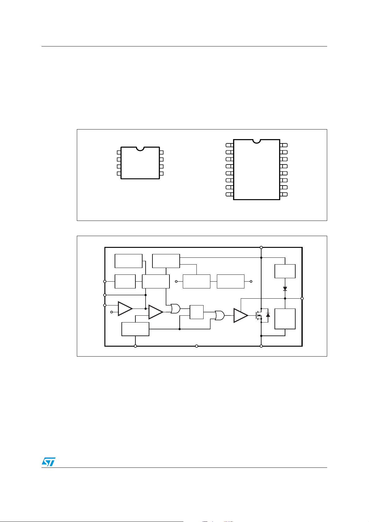
Figure 2 show s the two packaging options, with the pin function assignments.
Figure 2. Pin Connections
GND
SS_INH
OSC
OUT
1
2
3
4 VCC
D97IN595
DIP8
Figure 3. Block diagram.
THERMAL
SHUTDOWN
COMP
2
INHIBIT SOFTSTART
7
8
FB
E/A
3.3V
OSCILLATOR
SS_INH
7
6
5
VOLTAGES
MONITOR
PWM
FB8
COMP
BOOT
3.3V
INTERNAL
REFERENCE
R
Q
S
N.C.
GND
SS_INH
OSC
OUT
OUT
N.C.
N.C. N.C.
2
3
4
5
6
7
8
D97IN596
16
15
14
13
12
11
10
9
SO16L
VCC
5
CBOOT
INTERNAL
SUPPLY
5.1V
DRIVE
CHARGE
CBOOT
CHARGE
AT LIGHT
LOADS
N.C.1
N.C.
FB
COMP
BOOT
VCC
N.C.
6
BOOT
3
OSC GND OUT
1
Doc ID 5655 Rev 15 3/29
4
D97IN594
Power supply, UVLO and voltage reference AN937
2 Power supply, UVLO and voltage reference
The device is provided with an internal stabilized power supply (of about 12 V typ.) that
powers the analog and digital control blocks and the bootstrap section.
From this pre regulator, a 3.3V reference voltage ±2%, is internally available.
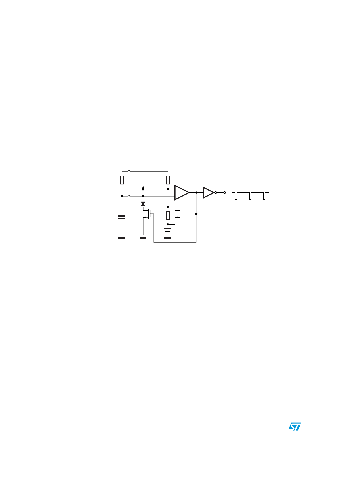
2.1 Oscillator and voltage feed forward
Just one pin is necessary to implement the oscillator function, with inherent voltage
feedforward.
Figure 4. Oscillator internal circuit
V
CC
R
OSC
TO PWM
COMPARATOR
Osc
5R
-
+
CLOCK
Q
1
C
OSC
Q
2
R
1V
D97IN655A
A resistor Rosc and a capacitor Cosc connected as shown in Figure 4, allow the setting of
the desired switching frequency in agreement with the below formula:
1
6
⎛⎞
---
⎝⎠
5
100 C
⋅+
osc
dson
Where F
is in kHz, R
sw
osc
The oscillator capacitor, C
F
in kΩ and C
osc
-------------------------------------------------------------------------------------=
SW
⋅()In
R
oascCosc
in nF.
osc
, is discharged by an internal MOS transistor of 100 Ω of R
(Q1) and during this period the internal threshold is set at 1 V by a second MOS, Q2. When
the oscillator voltage capacitor reaches the 1V threshold the output comparator turn-off the
MOS Q1 and turn-on the MOS Q2, restarting the C
charging.
osc
The oscillator block, shown in Figure 4, generates a sawtooth wave signal that sets the
switching frequency of the system.
This signal, compared with the output of the error amplifier, generates the PWM signal that
will modulate the conduction time of the power output stage.
The way the oscillator has been integrated, does not require additional external components
to benefit of the voltage feed forward function.
4/29 Doc ID 5655 Rev 15
AN937 Power supply, UVLO and voltage reference
The oscillator peak-to-valley voltage is proportional to the supply voltage, and the voltage
feed forward is operative from 8 V to 55 V of input supply.
VCC1–
osc
--------------------=
6
ΔV
Also the ΔV/Δt of the sawtooth is directly proportional to the supply voltage. As Vcc
increases, the Ton time of the power transistor decreases in such a way to provide to the
choke, and finally also the load, the product Volt. sec constant.
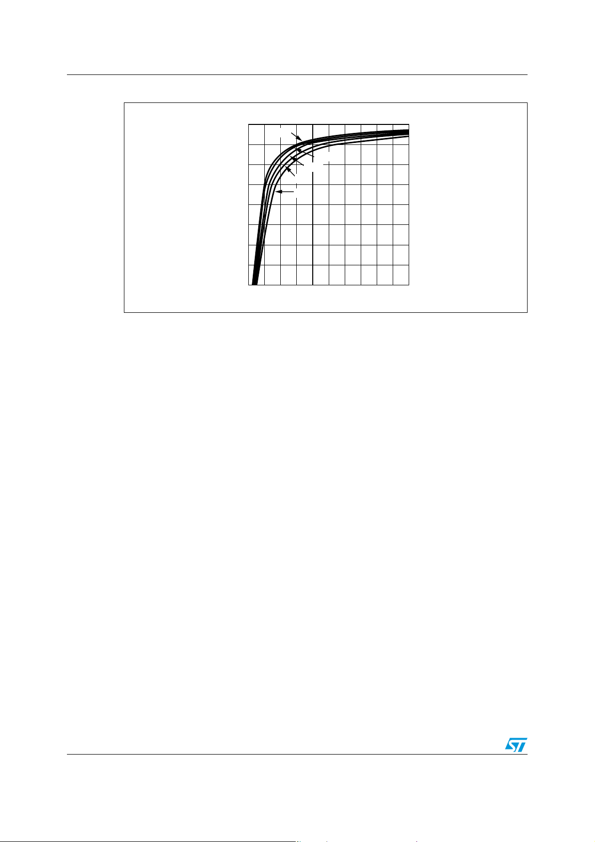
Figure 6 show how the duty cycle varies as a result of the change on the ΔV/Δt of the
sawtooth with the Vcc. The output of the error amplifier doesn’t change to maintain the
output voltage constant and in regulation. With this function on board, the output response
time is greatly reduced in presence of an abrupt change on the supply voltage, and the
output ripple voltage at the mains frequency is greatly reduced too.
Figure 5. Device switching frequency vs Rosc and Cosc
fsw
(KHz)
500
200
100
50
20
10
5
0 20 40 60 80 R2(KΩ)
0.82nF
Figure 6. Voltage feed forward function
V1
D97IN630
Tamb=25˚C
1.2nF
2.2nF
3.3nF
4.7nF
5.6nF
Vi=30V
Vi=15V
Vc
t
V2-3
Vi=30V
Vi=15V
t
D97IN684
Doc ID 5655 Rev 15 5/29
Power supply, UVLO and voltage reference AN937
Figure 7. Maximum duty cycle vs. Rosc and Cosc as parameter
D
max
0.90
0.80
0.70
0.60
5.3nF
4.7nF
2.2nF
1.2nF
0.8nF
0 4 8 121620242832R
D97IN685
OSC
(KΩ)
In fact, the slope of the ramp is modulated by the input ripple voltage, generally present in
the order of some tents of Volt, for both off-line and dc-dc converters using mains
transformers.
The charge and discharge time is approximately to:
6
⎛⎞
Tch R
⋅ In
oscCosc
---
⋅=
⎝⎠
5
The maximum duty cycle is a function of Tch, Tdis and an internal delay and is represented
by the equation:
and is represented in Figure 7:
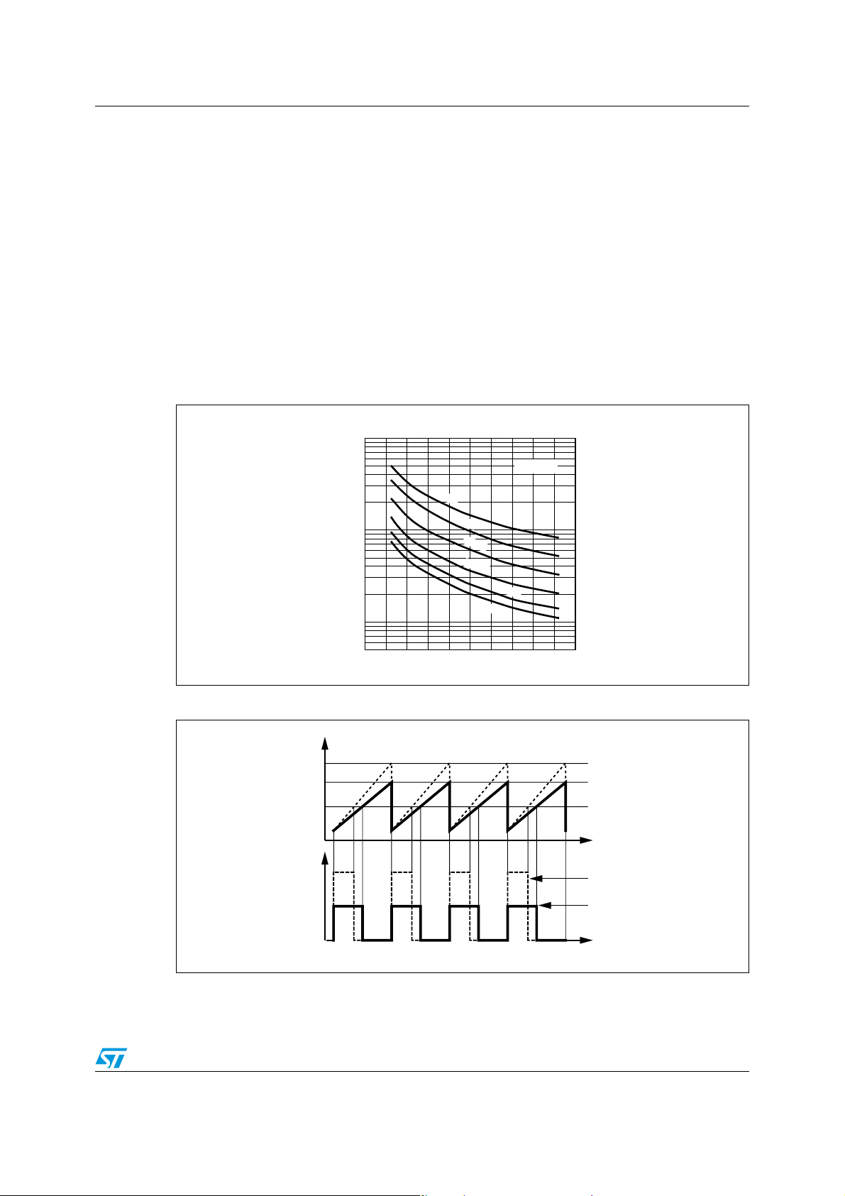
2.2 Current protection
The L4971 has two current limit levels, pulse by pulse and hiccup modes.
Increasing the output current till the pulse by pulse limiting current threshold (Ith1 typ. value
of 2.5 A) the controller reduces the on-time till the value of T
time in which the current limit protection does not trigger. This minimum time is necessary to
avoid undesirable intervention of the protection due to the spike current generated during
the recovery time of the freewheeling diode.
Dmax
Tdis 100 C
R
oscCosc
----------------------------------------------------------------------------------=
R
oscCosc
In
⋅=
In
⎛⎞
⎝⎠
osc
6
⎛⎞
---
⎝⎠
5
6
---
5
80 109–⋅–⋅⋅
100 C
⋅+⋅⋅
osc
= 300 ns that is a blanking
B
6/29 Doc ID 5655 Rev 15
AN937 Power supply, UVLO and voltage reference
In this condition, because of this fixed blanking time, the output current is given by:
I
max
---------------------------------------------------------------------------------------------------------------------------------------------------=
R
O
VCCTBF
RDRL+()1TBFSW⋅–()R
SWVf
1TBFSW⋅–()⋅–⋅⋅[]
+()TBFSW⋅++[]
dsonRL
In Figure 8, the pulse by pulse protection is sufficient to limit the current.
In Figure 9 the pulse by pulse protection is no more effective to limit the current due to the
minimum Ton fixed by the blanking time TB, and the hiccup protection intervenes because
the output peak current reaches the relative threshold. At the pulse by pulse intervention
(point A) the output voltage drops because of the Ton reduction, and the current is almost
constant. Going versus the short circuit condition, the current is only limited by the series
resistances RD and RL (see relation above) and could reach the hiccup threshold (point B),
set 20% higher than the pulse by pulse. Once the hiccup limiting current is operating, in
output short circuit condition, the delivered average output current decreases dramatically at
very low values (point C).
Figure 8. Output characteristics
V
O
A
C
D98IN908A
Figure 9. Output characteristics
V
O
D97IN809
2.5A
A
2.5A
3A
3A
B
I
O
I
O
Doc ID 5655 Rev 15 7/29
Power supply, UVLO and voltage reference AN937
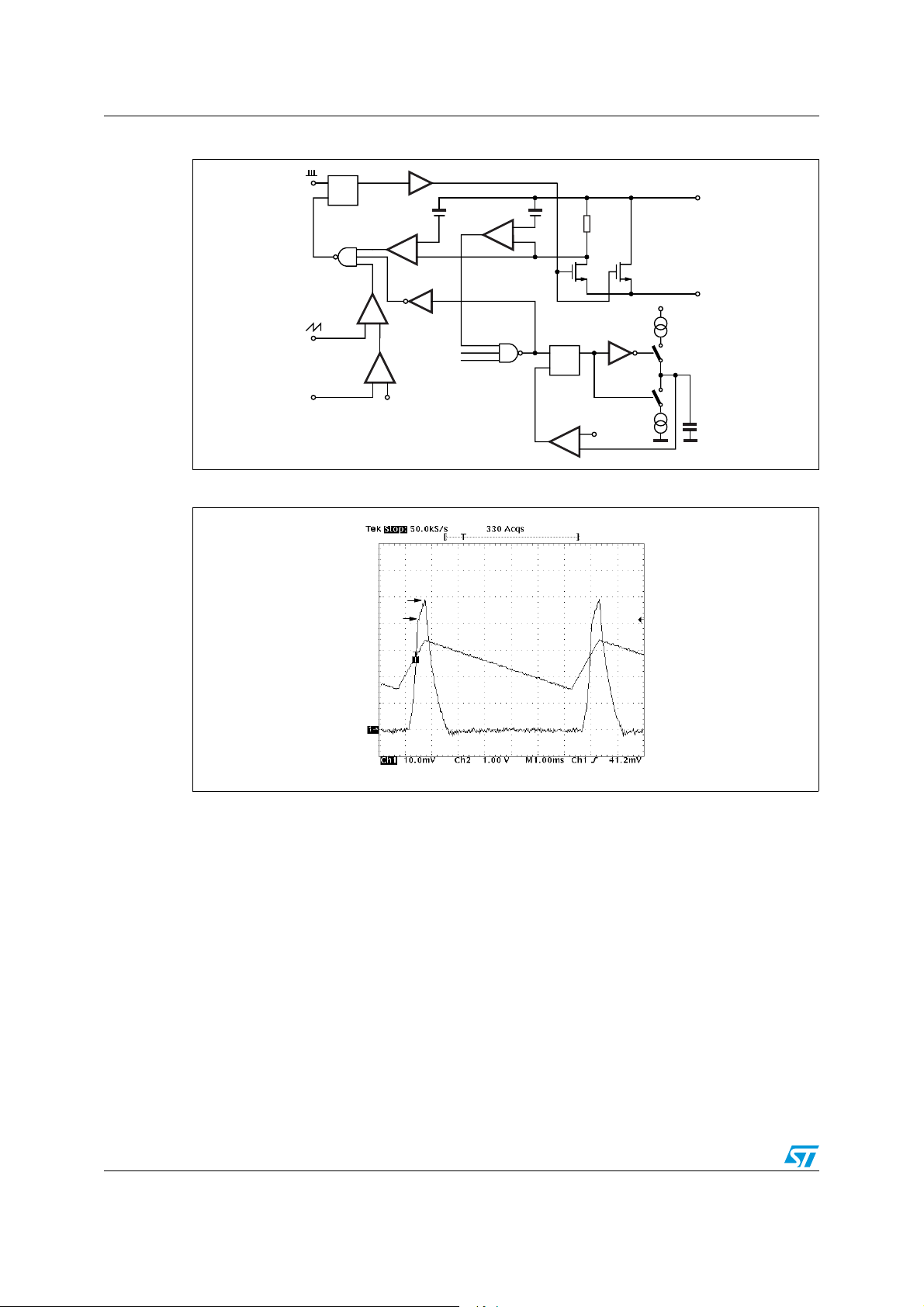
Figure 10. Current limiting internal schematic circuit
Q
S
OSC
R
V
Th1
+
-
V
Th2
+
-
V
CC
PWM
+-
OSC
VFB
THERMAL
+-
VREF
HICCUP
UNDERVOLTAGE
D97IN658
Figure 11. Output current and soft start voltage
5.4A
4.5A
SOFT START
LATCH
Q
S
R
+
-
OUT
12V
C
0.4
SS
Figure 10 shows the internal current limiting circuitry. Vth1 is the pulse by pulse while Vth2 is
the hiccup threshold.
The sense resistor is in series with a small MOS realized as a partition of the main DMOS.
The Vth2 comparator (20% higher than Vth1) sets the soft start latch, initializing the
discharge of the soft start capacitor with a constant current (about 22 mA). Reaching about
0.4 V, the valley comparator resets the soft start latch, restarting a new recharge cycle.
Figure 11 shows the typical waveforms of the current in the output inductor and the soft start
voltage (pin 2).
During the recharging of the soft start capacitor, the Ton increases gradually and, if the short
circuit is still present, when Ton>TB and the output peak current reaches the threshold, the
hiccup protection intervenes again. So, the value of the soft start capacitor must not be too
high (in this case the Ton increases slowly thus taking much time to reach the TB value) to
avoid that during the soft start slope, the current exceeds the limit before the protection
activation.
8/29 Doc ID 5655 Rev 15
AN937 Power supply, UVLO and voltage reference
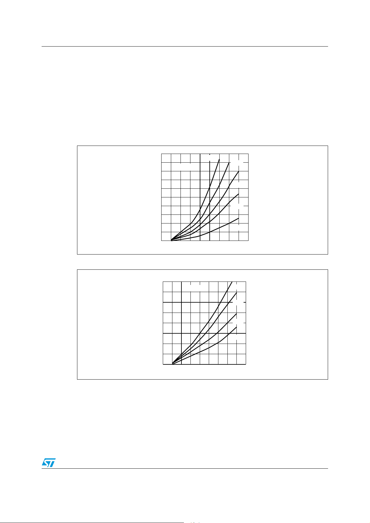
The following diagrams of Figure 13 and Figure 14 show the maximum allowed soft-start
capacitor as a function of the input voltage, inductor value and switching frequency. A
minimum value of the soft start capacitance is necessary to guarantee, in short circuit
condition, the functionality of the limiting current circuitry.
In fact, with a capacitor too small, the frequency of the current peaks (see Figure 11) is high
and the mean current value in short circuit increases.
Example: for a maximum input voltage of 55 V at 100 kHz, with an inductor of 260 mH, it is
possible to use a soft start capacitor lower than 470 µF. With such a value, the soft start time
(see Figure 19) of about 10 ms for an output voltage of 5 V.
Figure 12. Maximum soft start capacitance with f
L
(μH)
fsw=100KHz
400
300
200
100
0
15 20 25 30 35 40 45 50 V
680nF
Figure 13. Maximum soft start capacitance with f
L
(μH)
300
200
fsw=200KHz
= 100 kHz
sw
D97IN745
470nF
330nF
220nF
100nF
CCmax
= 200 kHz
sw
D97IN746
56nF
47nF
33nF
(V)
22nF
100
0
15 20 25 30 35 40 45 50 VCCmax(V)
Doc ID 5655 Rev 15 9/29

Power supply, UVLO and voltage reference AN937
2.3 Soft-start and inhibit functions
The soft start and the inhibit functions are designed using one pin only, pin2. Soft-start is
requested to initialize all internal functions with a correct start-up of the system without
overstressing the power stage, avoiding the intervention of the current protection, and
having an output voltage rising smoothly without output overshoots.
At Vcc Turn-on or having had an intervention of inhibit function, an initial 5 μA internal
current generator starts to charge the soft-start capacitor, from 0 V to about 1.8 V. From this
hysteretic threshold, a 40 μA current generator is activated, putting in off state the previous
generator.
Figure 14. Soft-start and inhibit functions internal circuit
12V
UNDERVOLTAGE PROT.
HICCUP PROT.
THERMAL PROT.
S
R
Q
Comp2
+
-
1.3V
40μA
S1
S2
10μA
5μA
S4
S3
Comp1
+
-
1.2V 1.8V
SS_INH
1KΩ
C
D97IN808A
SS
At this point, the output PWM starts, initiating the rising phase of the output voltage.
The soft-start capacitor is quickly discharged in case of:
● Thermal protection intervention
● Hiccup limiting current condition
● Supply voltage lower than UVLO off threshold.
The soft-start and inhibit schematic diagram is shown in Figure 14.
At device turn-on, the soft-start capacitor has no charge, with 0 V at its terminals.
From 0 V to 1.8 V, switch S3 is opened and S4 is closed.
Soft-start capacitor is charged with 5 μA.
At 1.8 V, comp1 change the output status, opening S4 and closing S3, and the device starts
to generate the PWM signal, rising smoothly the output voltage.
Till this moment, S2 is opened, S1 closed.
By closing S3, the soft-start capacitor is charged with 40μA reaching its saturation voltage.
This procedure is repeated at each Vcc turn-on.
10/29 Doc ID 5655 Rev 15

AN937 Power supply, UVLO and voltage reference
Figure 15. Timing diagram in inhibit, overcurrent and turn off condition
INHIBIT OVER-CURRENT TURN-OFF
V
SS/INH
1.8V
1.3V
1.2V
t
I
C
I
LIM
PWM
I
O
I
LIM
t
t
V
O
t
V
CC
UVLO
OFF
D97IN811
t
Doc ID 5655 Rev 15 11/29

Power supply, UVLO and voltage reference AN937
Figure 16. Start up sequence
V
CC
UVLO
ON
t
V
SS/INH
1.8V
t
t
t
I
C
PWM
V
O
t
1
t
2
D97IN812
Turning Vcc off, the soft-start capacitor is discharged with a constant 10 μA (S2 closed, S3
closed, S1 and S4 open), from the moment when Vcc is crossing the UVLO off threshold.
The final discharge value is 1.2 V. In case of the Css is discharged using an external
grounded element when the voltage at Css reaches the threshold of 1.3 V Comp2 resets the
flip flop, S1 is closed, S2 is opened and the 40 mA current generator is activated.
The external switch, sinking some mA, discharges the soft-start under the 1.2 V Comp1
threshold, opening S3 and closing S4. At this point the device is in disable, sourcing only 5
μA through pin 2. When the external grounding element is removed, the device restarts
charging the soft start capacitance, initially, with 5 μA till the voltage reaches the 1.8 V
threshold and Comp1 connects the 40 μA charging current generator. In case of thermal
shutdown or overcurrent protection intervention the power is turned off and the flip flop turns
off S2 and turns on S1. The soft-start is discharged till the voltage reaches the 1.3 V
threshold, and Comp2 resets the flip flop. S1 is closed, S2 is opened and the soft-start
capacitance is charged again.
Figure 15 shows the systems signals during Inhibit, overcurrent and Vcc turn off.
t1 and t2 can be calculated by the following equations:
t1 0.36 Css ;⋅= t2
12/29 Doc ID 5655 Rev 15
V
O
-----------------------------------
Ich 6 D
⋅⋅
max
⋅=
C
ss

AN937 Power supply, UVLO and voltage reference
where Dmax is 0.95, Css is in μF and Ich is in μA. Soft-start time (t2) versus output voltage
and Css is shown in Figure 17.
Thanks to the voltage feed forward, the start-up time (t2) is not affected by the input voltage.
Figure 18 shows the output voltage start-up using different soft-start capacitance values:
It is mandatory a minimum capacitor value of 22 nF. The pin 2 cannot be left open.
Figure 17. Soft-start time (t2) vs Vo and Css
t
ss
(ms)
70
60
50
40
30
20
10
0
0 3 6 9 12 15 18 21 24 VO(V)
D97IN687
1μF
470nF
330nF
220nF
100nF
Figure 18. Output rising voltage with Css 56 nF, 100 nF, 22 0nF
Doc ID 5655 Rev 15 13/29

Power supply, UVLO and voltage reference AN937
2.4 Feedback disconnection
In case of feedback disconnection, the duty cycle increases versus the max allowed value
bringing the output voltage close to the input supply. This condition could destroy the load.
To avoid this dangerous condition, the device is forcing a little current (1.4 μA typical) out of
the pin 8 (E/A Feedback).
If the feedback is disconnected, open loop, and the impedance at pin 8 is higher than 3.5
MΩ, the voltage at this pin goes higher than the internal reference voltage located on the
non-inverting error amplifier input, and turns-off the power device.
2.5 Zero load
In normal operation, the output regulation is also guaranteed because the bootstrap
capacitor is recharged, cycle by cycle, by means of the energy flowing into the choke.
Under light load conditions, this topology tends to operate in burst mode, with random
repetition rate of the bursts. An internal new function makes this device capable of keeping
the output voltage in full regulation with 1mA of load current only.
Between 1 mA and 500 μA, the output is kept in regulation up to 8% above the nominal
value.
Here the circuitry providing the control:
1. A comparator located on the bootstrap section is sensing the bootstrap voltage; when
this is lower than 5 V, the internal power VDMOS is forced ON for one cycle and OFF
for the next.
2. During this operation mode, i.e. 500 μA of load current, the E/A control is lost. To avoid
output over voltage, a comparator with one input connected to pin 8, and the second
input connected to a threshold 8% higher that nominal output, turns OFF the internal
power device the output is reaching that threshold.
When the output current, or rather, the current flowing into the choke, is lower than 500
μA, that is also the consumption of the bootstrap section, the output voltage starts to
increase, approaching the supply voltage.
2.6 Output overvoltage protection (OVP)
The output overvoltage protection, OVP, is realized by using an internal comparator, which
input is connected to pin 8, the feedback, that turns-off the power stage when the OVP
threshold is reached. This threshold is typically 8% higher than the feedback voltage.
When a voltage divider is requested for adjusting the output voltage, the OVP intervention
will be set at:
Ra Rb+()
V
OVP
1.08 V
⋅⋅=
---------------------------
fB
Rb
where Ra is the resistor connected to the output.
14/29 Doc ID 5655 Rev 15

AN937 Power supply, UVLO and voltage reference
2.7 Power stage
The power stage is realized by a N-channel D-MOS transistor with a Vdss in excess of 60 V
and typ R
Minimizing the R
But also the switching losses have to be taken into consideration. mainly for the two
following reasons:
a) They are affecting the system efficiency and the device power dissipation
b) Because they generate EMI.
of 290 mΩ (measured at the device pins).
dson
, means also minimize the conduction losses.
dson
2.8 Turn - on
At turn-on of the power element, or better, the rise time of the current (di/dt) at turn-on is the
most critical parameter to compromise.
At a first approach, it looks that faster is the rise time and lower are the turn-on losses.
It’s not completely true.
There is a limit, and it’s introduce by the recovery time of the recirculation diode.
Above this limit, about 100 A/usec, only disadvantages are obtained:
1. Turn-on overcurrent is decreasing efficiency and system reliability
2. Big EMI increase.
The L4971 has been developed with a special focus on this dynamic area.
An innovative and proprietary gate driver, with two different timings, has been introduced.
When the diode reverse voltage is reaching about 3 V, the gate is sourced with low current
(see Figure 20) to assure the complete recovery of the diode without generating unwanted
extra peak currents and noise. After this threshold, the gate drive current is quickly
increased, producing a fast rise time till the peak current, so maintaining the efficiency very
high.
Figure 19. Turn on and Turn off (pin 2, 3)
Doc ID 5655 Rev 15 15/29

Power supply, UVLO and voltage reference AN937
Figure 20. Power stage internal circuit
C
SS
V
Q
3
I
1
Q
4
I
4
I
5
I
2
Q
5
I
3
from PWM LATCH
i
Q
1
C
S
Q
2
SS
L
S
RS
+
CD
V
O
-
2.9 Turn - off
The turn-off behavior, is shown at Figure 19.
Figure 20 shows the details of the internal power stage and driver, where at Q2 is
demanded the turn-off of the power switch, S.
DELAY
D97IN659
16/29 Doc ID 5655 Rev 15

AN937 Typical application
3 Typical application
Figure 22 shows the typical application circuit, where the input supply voltage, Vcc, can
range from 8 to 55 V operating, and the output voltage adjustable from 3.3 V to 40 V.
The selected components, and in particular input and output capacitors, are able to sustain
the device voltage ratings, and the corresponding RMS currents.
3.1 Electrical specification
● Input voltage range: 8 V - 55 V
● Output voltage: 5.1 V ±3% (Line, load and thermal)
● Output ripple: 51 mV
● Output current range: 1 mA - 1.5 A
● Max output ripple current: 30% Iomax
● Max output current: 1.5 A
● Switching frequency: 200 kHz
Figure 21. Application circuit
VINVIN
R1
220nC2220n
63V
1 2
JP1
JP1
C2
JUMPER
JUMPER
2.2nC32.2n
12kR112k
C3
C1
C1
180u 63v
180u 63v
INHINH
GNDGND
EKY-630ELL181MJ20S
3.2 Input capacitor
The input capacitor has to be able to support the max input operating voltage of the device
and the max rms input current. The input current is squared and the quality of these
capacitors has to be very high to minimize its power dissipation generated by the internal
ESR, improving the system reliability. Moreover, input capacitors are also affecting the
system efficiency.
220nC6220n
OUT
VFB
100V
C11
C11
100n
100n
VOUTVOUT
GNDGND
L1
4
8
D1STPS3L60 D1STPS3L60
2 1
DO-201AD
L1
120uH (CC MSS1260-124KLD)
120uH (CC MSS1260-124KLD)
C9
4.7nC94.7n
R5R5
C8C8
R2
2.7kR22.7k
R3
4.99kR34.99k
EKY-350ELL151MHB51
C10
C10
150uF
150uF
C7 100nC7 100n
R4
15kR415k
C4
22nC422n
6
BOOT
GND
1
5
U1L4971 DIP 8 U1L4971 DIP 8
C5
82pC582p
VCC
OSC
SS/INH
COMP
7
3
2
C6
The max Irms current flowing through the input capacitors is:
Doc ID 5655 Rev 15 17/29

Typical application AN937
I
rmsIO
2D2⋅
D
---------------–
η
2
D
-------+⋅=
2
η
where η is the expected system efficiency, D is the duty cycle and Io the output dc current.
This function reaches the maximum value at D = 0.5 and the equivalent rms current is equal
to Io/2. The following diagram Figure 23 is the graphical representation of the above
equation, with an estimated efficiency of 85%, at different output currents.
The maximum and minimum duty cycles are:
D
max
VOVf+
----------------------------- 0.66==D
+
V
ccminVf
max
VOVf+
------------------------------- 0.1==
V
+
ccmaxVf
where Vf is the freewheeling diode forward voltage. This formula is not taking into account
the power MOS Rdson, considering negligible the inherent voltage drop, respect input and
output voltages. At full load, 1.5 A, and D=0.5, the rms capacitor current to be sustained is of
0.75 A.
The selected 180 μF/63 V KY, guarantying a life time of 10000 hours at an ambient
temperature of 105°C and switching frequency of 100 kHz, can support 1.15 A RMS current.
Figure 22. Efficiency vs. output current
(%)
90
η
VCC=12V
D97IN738
VCC=8V
85
VCC=24V
80
75
70
65
60
0.0 0.2 0.4 0.6 0.8 1.0 1.2 1.4 IO(A)
VCC=48V
fsw=100KHz
=5.1V
V
O
18/29 Doc ID 5655 Rev 15

AN937 Typical application
Figure 23. Input capacitance rms current vs. duty cycle
I
RMS
0.75
0.5
0.25
0
0.1 0.2 0.3 0.4 0.5 0.6 0.7 0.8 D
3.3 Output voltage selection
An external voltage divider is required to set the regulated output voltage: I
where V
REF
is 3.3 V
VoV
IO=1.5A
IO=1.2A
IO=1A
IO=0.5A
IO=0.2A
⎛⎞
1
⋅=
REF
⎝⎠
R2
--------+
R3
D97IN801
3.4 Inductor selection
The criteria used in fixing the inductor value has been dictated by the wanted output ripple
voltage, 51mV max., performance obtained of course in combination with output capacitors
too.
The inductor ripple current, fixed at 30% of Iomax, i.e., 0.45 A, requires an inductor value of:
Equation 1
It is possible to plot as a function of Vo and Vccmax at 150 kHz and 200 kHz (see Figure 24
and Figure 25)
LOV
1D
–()
---------------------------
⋅=
O
ΔI
⋅
Lfsw
min
Doc ID 5655 Rev 15 19/29

Typical application AN937
Figure 24. Ideal inductor value requested for 30% ripple current, as a function of
max. input voltage and output (f
180
162
144
126
108
90
Lo (uH)
72
54
36
18
0
0 5 10 15 20 25 30 35 40 45
Vin = 15V
Vin = 20V
Vin = 25V
Vin = 30V
Vin = 35V
Vin = 40V
Vin = 45V
=150 kHz)
SW
Vout
Figure 25. Ideal inductor value requested for 30% ripple current, as a function of
max. input voltage and output (f
140
126
112
98
84
70
Lo (uH)
56
42
28
14
0
0 5 10 15 20 25 30 35 40 45
=
=200 kHz)
SW
Vin
The 120 µH value of the selected inductor is useful to keep the current ripple below
0.3*I
over the input / output voltage range operating at 200 kHz.
LOAD
20/29 Doc ID 5655 Rev 15

AN937 Typical application
3.5 Output capacitors
The output capacitors selection, Co, is mainly driven by the output ripple voltage that has to
be guaranteed, in this case 1% max. of Vo.
The output ripple is defined by the ESR of Co and by the ripple current flowing through it.
The output capacitance is of 150 μF/35 V KY (Nippon Chemi-con), having an ESR of 150
mΩ at 20 °C. The ideal ripple voltage over the input voltage range is shown in Figure 26.
Figure 26. Ideal ripple voltage as a function of input and output voltage (f
SW
=200
kHz)
90
82
74
66
58
50
Vripple (mV)
42
34
26
18
10
10 15 20 25 30 35 40 45
Vout = 1.5V
Vout = 2.5V
Vout = 3.3V
Vout = 5V
Vout = 12V
51 mV
Vin
Co has also to support load transients. An idea of the magnitude of the output voltage drop
during load transients is given below:
Equation 2
ΔIO()2LO⋅
OVinminDmaxVO
–⋅()⋅⋅
where ΔI
ΔV
is the load current change, from 0.5 A to 1.5 A, Dmax is the max. duty cycle, 95%,
o
--------------------------------------------------------------------------=
O
2C
Vo nominal is 5.1 V, and finally L is 68 μH.
Equation 2, normalized at Vo, is represented in the following diagram, Fig. 27, as a function
of the minimum input voltage.
These curves are represented for different output capacitor 2x150 μF, 2x220 μF, 2x330 μF
all KY, 35 V.
Doc ID 5655 Rev 15 21/29

Typical application AN937
3.6 Compensation network
The complete control loop block diagram is shown in Figure 29. The error amplifier basic
characteristics are:
gm = 2.5mS
Ro = 1.2MΩ
Avo = 60dB
Isource/sink = 300 μA
Figure 27. Output drop (%) vs minimum input voltage
3.5
3
2.5
2
dVo / Vo (%)
1.5
1
0.5
0
10 15 20 25 30 35 40 45
Cout = 1 x 150uF
Cout = 2 x 150uF
Cout = 3 x 150uF
Vin
Figure 28. Block diagram compensation loop
V
REF
+-
A(s) Vc/Vct LC
α
Cc
Rogm
Rc
Co
D97IN698
L
D97IN697
Avo=gm·R
V
O
o
22/29 Doc ID 5655 Rev 15
Cout
Resr
D97IN700

AN937 Typical application
3.7 Error amplifier and compensation blocks
The open loop gain is:
1sRcC
As() gm
R
----------------------------------------------------------------------------------------------------------------------------------------------------
⋅=
2
s
RoCoRcCcsRoCcRoCoRcCc⋅+⋅+⋅()1+⋅+⋅⋅⋅⋅
O
⋅⋅+()⋅
c
where Cout is the parallel between the output and the external capacitance of the Error
Amplifier and Ro the E/A output impedance. Rc and Cc are the compensation values.
3.8 LC filter
1R
out
esrCout
s2R
esr
A
os()
-----------------------------------------------------------------=
LC
3.9 PWM gain
CC
ct
VCC6⋅
--------------------
V
CC
1–
V
-----------
V
where Vct is the peak to peak sawtooth oscillator.
3.10 Voltage divider and leading network
Poles and zeros value are:
A
os()
R
3
--------------------
R2R3+
1R
-------------------------------------------------
⋅=
1s
R
--------------------
⋅⋅+
R
s⋅⋅+
s1+⋅+⋅⋅
6≈=
⋅+
2C9
⋅
2R3
+
2R3
C
9
F
o
---------------------------------------
F
p
2 π LC
F
ocomp
1
---------------------------------------
2 πR
⋅⋅
esrCout
1
⋅⋅⋅
out
1
---------------------------------
⋅⋅ ⋅
2 π R
cCc
------------------------------------------------------------- 8.2K Hz== =
2 π 0.130 150 10
⋅⋅ ⋅ ⋅
----------------------------------------------------------------------------- 1.2 kHz== =
2 π 120 10
---------------------------------------------------------------- 492Hz== =
2 π 15 10
⋅⋅ ⋅ ⋅ ⋅
1
6–
1
6–
150 10
⋅⋅⋅⋅⋅
6–
1
3
22 10
9–
Doc ID 5655 Rev 15 23/29

Typical application AN937
1
6
22 10
9–
1
12–
1
3
4.7 10
9–
1
3
4.7 10
9–
F
F
p1
F
p2
F
oLN
------------------------------------------------
pLN
2 π
⋅⋅ ⋅
1
----------------------------------
⋅⋅ ⋅
2 π R
oCc
1
----------------------------------
⋅⋅ ⋅
2 π R
cCo
1
----------------------------------
⋅⋅ ⋅
2 π R
2C9
1
R2R3⋅
--------------------
R
+
2R3
----------------------------------------------------------------- 6.029Hz== =
2 π 1.2 10
⋅⋅ ⋅ ⋅ ⋅
------------------------------------------------------------------ 125K Hz== =
2 π 15 10382 10
⋅⋅ ⋅ ⋅ ⋅
------------------------------------------------------------------- 12 KHz== =
2 π 2.7 10
⋅⋅ ⋅ ⋅ ⋅
---------------------------------------------------------------------- 19K Hz== =
⋅⋅ ⋅ ⋅ ⋅
2 π 1.75 10
C
9
Using a compensation network with R4= 15 kΩ, C4 = 22 nF and C5 = 82 pF, the gain and
Phase Bode plots are shown in Fig. 31-32. The cut-off frequency and the phase margin are:
= 3.3V Fc = 36KHz Phase margin = 62°
V
OUT
V
= 5V Fc = 34KHz Phase margin = 70°
OUT
V
= 12V Fc = 18KHz Phase margin = 92°
OUT
V
= 15V Fc = 14KHz Phase margin = 88°
OUT
V
= 18V Fc = 11KHz Phase margin = 83°
OUT
V
= 24V Fc = 8.6KHz Phase margin = 74°
OUT
Figure 29. Gain Bode plot open loop
90
79
68
57
46
35
Module [dB]
24
13
2
9
20
0.1 1 10 100 1.10
Vout=3.3V
Vout=5V
Vout=12V
Vout=15V
Vout=18V
Vout=24V
0 dB
Frequency [Hz]
3
1.10
4
1.10
5
1.10
6
24/29 Doc ID 5655 Rev 15

AN937 Typical application
Figure 30. Phase Bode plot open loop
180
157.5
135
112.5
90
Phase
67.5
45
22.5
0
0.1 1 10 100 1.10
Vout=3.3V
Vout=5V
Vout=12V
Vout=15V
Vout=18V
Vout=24V
EXTERNAL LOOP GAIN PHASE
Frequency [Hz]
3
1.10
4
1.10
5
1.10
6
Table 1. Component list (fsw = 200 kHz, V
OUT
= 5 V)
Reference Description Part number Manufacturer
R1 Resistor 12 KΩ 1% 1/4W
R2 Resistor 2.7 KΩ 1% 1/4W
R3 Resistor 4.99 KΩ 1% 1/4W
R4 Resistor 15 KΩ 1% 1/4W
R5 Not mounted
C1 Capacitor 180 μF 63V EKY-630ELL181MJ20S Nippon Chemi-con
C2 - C6 Capacitor 220 nF 63V
C3 Capacitor 2.2 nF 100V
C4 Capacitor 22 nF 50V
C5 Capacitor 82 pF 50V
C7 - C11 Capacitor 100 nF 100V
C8 Not mounted
C9 Capacitor 4.7 nF 50V
C10 Capacitor 150 μF 35V EKY-350ELL151MHB5D Nippon Chemi-con
L1 120 μH I
= 1.85A I
RMS
= 1.92A MSS1260-124KLD Coilcraft
SAT
U1 L4971 STMicroelectronics
Doc ID 5655 Rev 15 25/29

Typical application AN937
Table 2. Resistor divider for V
Reference Description Part number Manufacturer
R2 Resistor 2.7 kΩ 1%
R3 Resistor 1 kΩ 1%
Table 3. Resistor divider for V
Reference Description Part number Manufacturer
R2 RESISTOR 2.7 KΩ 1%
R3 NOT MOUNTED
OUT
OUT
=12 V
=3.3 V
Figure 31. Evaluation board (components side)
26/29 Doc ID 5655 Rev 15

AN937 Typical application
Figure 32. Evaluation board (bottom side)
Figure 33. Evaluation board (top side)
Doc ID 5655 Rev 15 27/29

Revision history AN937
4 Revision history
Table 4. Document revision history
Date Revision Changes
October 2004 13 First Issue in EDOCS
May 2005 14
03-May-2011 15 Updated the evaluation board description
Updated the Layout look & feel.
Changed name of the D1 on the fig. 21
28/29 Doc ID 5655 Rev 15

AN937
Please Read Carefully:
Information in this document is provided solely in connection with ST products. STMicroelectronics NV and its subsidiaries (“ST”) reserve the
right to make changes, corrections, modifications or improvements, to this document, and the products and services described herein at any
time, without notice.
All ST products are sold pursuant to ST’s terms and conditions of sale.
Purchasers are solely responsible for the choice, selection and use of the ST products and services described herein, and ST assumes no
liability whatsoever relating to the choice, selection or use of the ST products and services described herein.
No license, express or implied, by estoppel or otherwise, to any intellectual property rights is granted under this document. If any part of this
document refers to any third party products or services it shall not be deemed a license grant by ST for the use of such third party products
or services, or any intellectual property contained therein or considered as a warranty covering the use in any manner whatsoever of such
third party products or services or any intellectual property contained therein.
UNLESS OTHERWISE SET FORTH IN ST’S TERMS AND CONDITIONS OF SALE ST DISCLAIMS ANY EXPRESS OR IMPLIED
WARRANTY WITH RESPECT TO THE USE AND/OR SALE OF ST PRODUCTS INCLUDING WITHOUT LIMITATION IMPLIED
WARRANTIES OF MERCHANTABILITY, FITNESS FOR A PARTICULAR PURPOSE (AND THEIR EQUIVALENTS UNDER THE LAWS
OF ANY JURISDICTION), OR INFRINGEMENT OF ANY PATENT, COPYRIGHT OR OTHER INTELLECTUAL PROPERTY RIGHT.
UNLESS EXPRESSLY APPROVED IN WRITING BY AN AUTHORIZED ST REPRESENTATIVE, ST PRODUCTS ARE NOT
RECOMMENDED, AUTHORIZED OR WARRANTED FOR USE IN MILITARY, AIR CRAFT, SPACE, LIFE SAVING, OR LIFE SUSTAINING
APPLICATIONS, NOR IN PRODUCTS OR SYSTEMS WHERE FAILURE OR MALFUNCTION MAY RESULT IN PERSONAL INJURY,
DEATH, OR SEVERE PROPERTY OR ENVIRONMENTAL DAMAGE. ST PRODUCTS WHICH ARE NOT SPECIFIED AS "AUTOMOTIVE
GRADE" MAY ONLY BE USED IN AUTOMOTIVE APPLICATIONS AT USER’S OWN RISK.
Resale of ST products with provisions different from the statements and/or technical features set forth in this document shall immediately void
any warranty granted by ST for the ST product or service described herein and shall not create or extend in any manner whatsoever, any
liability of ST.
ST and the ST logo are trademarks or registered trademarks of ST in various countries.
Information in this document supersedes and replaces all information previously supplied.
The ST logo is a registered trademark of STMicroelectronics. All other names are the property of their respective owners.
© 2011 STMicroelectronics - All rights reserved
STMicroelectronics group of companies
Australia - Belgium - Brazil - Canada - China - Czech Republic - Finland - France - Germany - Hong Kong - India - Israel - Italy - Japan -
Malaysia - Malta - Morocco - Philippines - Singapore - Spain - Sweden - Switzerland - United Kingdom - United States of America
www.st.com
Doc ID 5655 Rev 15 29/29
 Loading...