

Page 1
AN934
Application note
How to use the digital calibration feature in
TIMEKEEPER
Introduction
The term “quartz accurate” has become a familiar phrase used to describe the accuracy of
many time keeping functions. Quartz oscillators provide an accuracy far superior to other
conventional oscillator designs, but they are not perfect. Quartz crystals are sensitive to
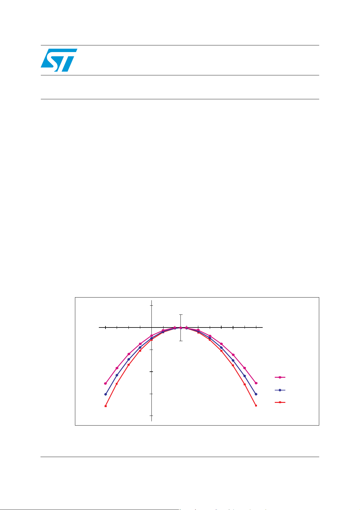
temperature variations. Figure 1 shows the relationship between accuracy (acc),
temperature (T), and curvature (K) for the 32,768Hz crystal used on STMicroelectronics
TIMEKEEPER
®
products. The curves follow this general formula:
®
and serial real-time clock (RTC) products
acc K T TO–()
×=
2
where T
= 25 °C ± 5 °C and K = –0.036 ppm/°C2 ± 0.006 ppm/°C2.
O
The clocks used in most applications require a high degree of accuracy, and there are
several factors involved in achieving this accuracy. Typically most crystals are compensated
by adjusting the load capacitance of the oscillator. This method, while effective, has several
disadvantages:
1. It requires external components (trim capacitors); and
2. it can increase oscillator current (an important factor in battery-supported applications).
STMicroelectronics replaced this crude analog method with a digital calibration feature. This
method gives the user software control over the calibration procedure which makes it user
friendly.
Figure 1. Typical crystal accuracy plotted against temperature (and against
different values of K)
50
+35 ppm
–30
–20
–10
–50
–100
10
0
30
20
–35 ppm
50 60 70 80
Temperature (°C)
9040–40
Minimum K at 25°C
Typical K at 25°C
–150
–200
Accuracy (ppm)
Maximum K at 25°C
AI02498
October 2011 Doc ID 6393 Rev 4 1/14
www.st.com
Page 2

Contents AN934
Contents
Methodology . . . . . . . . . . . . . . . . . . . . . . . . . . . . . . . . . . . . . . . . . . . . . . . . . . . . . . . . 4
Calculating the needed amount of calibration . . . . . . . . . . . . . . . . . . . . . . . . . . . . . 7
Calculating calibration over a temperature range . . . . . . . . . . . . . . . . . . . . . . . . . . 8
Calculating the calibration for multiple operating temperatures . . . . . . . . . . . . . . 9
Enabling the frequency test function (FT) . . . . . . . . . . . . . . . . . . . . . . . . . . . . . . . 10
Conclusion. . . . . . . . . . . . . . . . . . . . . . . . . . . . . . . . . . . . . . . . . . . . . . . . . . . . . . . . . 12
Revision history . . . . . . . . . . . . . . . . . . . . . . . . . . . . . . . . . . . . . . . . . . . . . . . . . . . . 13
2/14 Doc ID 6393 Rev 4
Page 3

AN934 List of figures
List of figures
Figure 1. Typical crystal accuracy plotted against temperature (and against different values of K) . . 1
Figure 2. Oscillator divider chain . . . . . . . . . . . . . . . . . . . . . . . . . . . . . . . . . . . . . . . . . . . . . . . . . . . . . 4
Figure 3. Clock splitting and clock blanking . . . . . . . . . . . . . . . . . . . . . . . . . . . . . . . . . . . . . . . . . . . . . 4
Figure 4. Control register . . . . . . . . . . . . . . . . . . . . . . . . . . . . . . . . . . . . . . . . . . . . . . . . . . . . . . . . . . . 5
Figure 5. Crystal accuracy over a temperature range . . . . . . . . . . . . . . . . . . . . . . . . . . . . . . . . . . . . . 8
Figure 6. A day of the week register (for parallel devices) . . . . . . . . . . . . . . . . . . . . . . . . . . . . . . . . . 10
Figure 7. 512 Hz output to DQ0 . . . . . . . . . . . . . . . . . . . . . . . . . . . . . . . . . . . . . . . . . . . . . . . . . . . . . 10
Doc ID 6393 Rev 4 3/14
Page 4
Methodology AN934
Methodology
The STMicroelectronics TIMEKEEPER® products are driven by a quartz crystal-controlled
oscillator with a nominal frequency of 32.768 kHz. The crystal is mounted in either a 600 mil
DIP CAPHAT™ package, 600 mil DIP hybrid, 300mil SOIC embedded crystal, or in a
330 mil SOIC SNAPHAT
accurate within ±1.53 minutes (±35 ppm - parts per million) per month at 25 °C without
calibration.
Two sources of clock error are:
● temperature variation
● crystal variation
As mentioned previously, most clock chips compensate for crystal frequency and
temperature shift error with cumbersome “trim” capacitors. The TIMEKEEPER design
employs periodic counter correction. The digital calibration circuit adds or subtracts counts
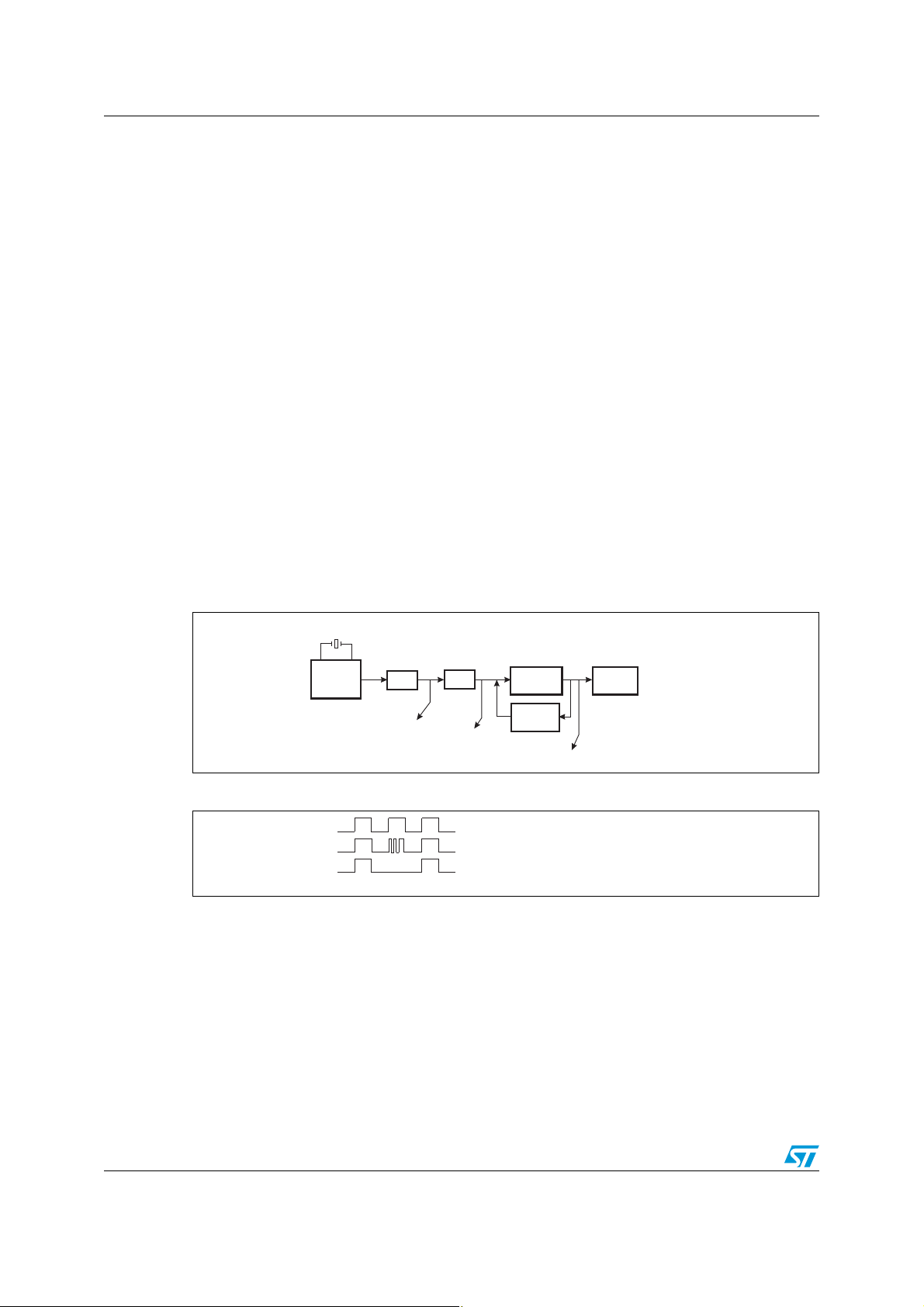
from the oscillator divider circuit at the 256 Hz stage (see Figure 2).
Figure 3 shows how extra clock pulses are added (by clock splitting) or removed (by clock
blanking). The number of times the pulses are split (added during positive calibration) or
blanked (subtracted during negative calibration) depends upon the value that has been
loaded into the least significant five bits of the control register. Adding counts speeds the
clock up while subtracting counts slows the clock down.
®
package, along with the battery. A typical TIMEKEEPER device is
Figure 2. Oscillator divider chain
32768Hz
Low
Current
Oscillator
512Hz Output
for Frequency Test
div 64
div 2
256Hz
Calibration
64 Minute
Figure 3. Clock splitting and clock blanking
No Calibration
Positive Clock Calibration
Negative Clock Calibration
Circuitry
Cycle
1Hz Signal
Clock
Registers
AI02801
AI02800
4/14 Doc ID 6393 Rev 4
Page 5
AN934 Methodology
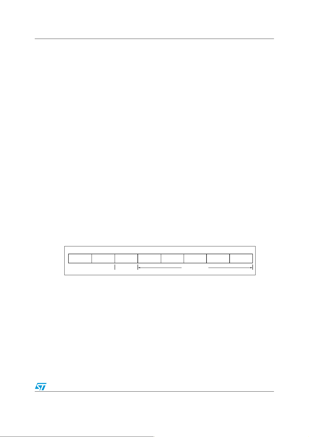
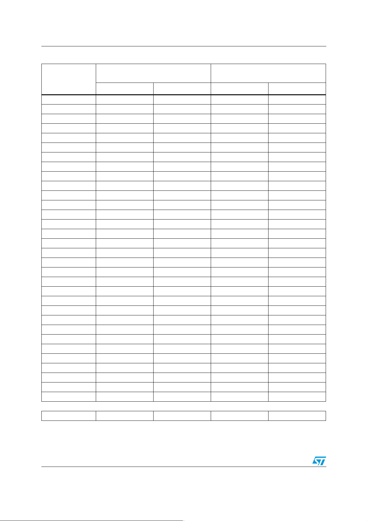
The calibration byte occupies the five lower order bits in the control register, as shown in
Figure 4. These bits represent the binary value between 0 and 31. Table 1 on page 6 shows
how many seconds (or ppm) each bit represents in real time for the TIMEKEEPER
®
product
line. The sixth bit is a sign bit. A binary '1' indicates a positive calibration (added pulses), and
a binary '0' indicates a negative calibration (blanked pulses). Calibration occurs within a 64minute cycle. The first 62 minutes in the cycle may, once per minute, have one second either
shortened by 128 or lengthened by 256 oscillator cycles. If a binary '1' is loaded into the
register, only the first 2 minutes in the 64-minute cycle are modified; if a binary “6” is loaded,
the first 12 minutes are affected, and so on.
Therefore, each calibration step has the effect of adding 512 or subtracting 256 oscillator
cycles for every 125,829,120 actual oscillator cycles (64 minutes x 60 seconds/minute x
32,768 cycles/second). That is, +4.068 or –2.034 ppm of adjustment per calibration step in
the calibration register. Assuming that the oscillator is running exactly at 32.768kHz, each of
the 31 increments in the calibration byte represent +10.7 or –5.35 seconds per month, which
corresponds to a total range of +5.5 or –2.75 minutes per month.
As can be seen from Figure 1 on page 1, the peak of the curve corresponds to
approximately 25 °C. This is known as the “turnover temperature.” As the temperature rises
or falls from room temperature, the oscillator slows down. Typically the turnover point on the
graph is very close to 32.768 kHz (no error). However, variations from one crystal to another
may cause the turnover point to be slightly above or below 32.768 kHz. The frequency
variation for an uncalibrated device is a function of the crystal frequency variation for the
given load capacitance (C
). Thus, if the crystal has a CL that is different from the actual
L
internal load capacitance of the device, then the oscillator frequency will run faster or slower
than the 32.768 kHz (±1 Hz). At STMicroelectronics, the real-time clock has an internal
capacitance of 12.5 pF (except for the M41T6x series, which has an internal capacitance of
6 pF) across the crystal input pins. For this reason, the calibration feature can be
programmed to adjust for both negative and positive variations. Entering a value into the
6-bit calibration field of the control register will shift the entire curve up or down according to
the values found in Table1 on page6.
Figure 4. Control register
d7
(1)
x
AI05651
1. x = W (Parallel device); OUT (Serial device)
2. y = R (Parallel device); FT (Serial device)
d6
(2)
y
d5
S
Sign Bit
d4
Doc ID 6393 Rev 4 5/14
d3
d2
Calibration Value
d1
d0
Page 6
Methodology AN934
Table 1. Calibration table: compensation values in seconds per month (30 days) and in ppm
Calibration
value (binary)
00000 0 0 0 0
00001 11 5 4 2
00010 21 11 8 4
00011 32 16 12 6
00100 42 21 16 8
0010153262010
0011063322412
0011174372814
0100084423316
0100195473718
01010 105 53 41 20
01011 116 58 45 22
01100 127 63 49 24
01101 137 69 53 26
01110 148 74 57 29
01111 158 79 61 31
10000 169 84 65 33
10001 179 90 69 35
10010 190 95 73 37
10011 200 100 77 39
10100 211 105 81 41
10101 221 111 85 43
10110 232 116 89 45
10111 243 121 93 47
11000 253 127 98 49
11001 264 132 102 51
11010 274 137 106 53
11011 285 142 110 55
11100 295 148 114 57
11101 306 153 118 59
11110 316 158 122 61
11111 327 163 126 63
In general:
N 337*N/32 169*N/32 337*N/(32*2.592) 169*N/(32*2.592)
Value in seconds per month (30 days)
rounded to the nearest second
Plus Minus Plus Minus
rounded to the nearest ppm
Value in ppm
6/14 Doc ID 6393 Rev 4
Page 7

AN934 Calculating the needed amount of calibration
Calculating the needed amount of calibration
There are two methods for establishing how much calibration are required in a given
application.
The first method can be easily implemented in the user environment simply by setting the
clock to a known accurate reference and then storing the time in some unused location in
the RAM. Over a period of time (30 days), the reference time is compared to the current time
(the average ambient temperature should be considered as well). This will tell the user how
fast or slow the clock operates for a period of 30 days. While it may seem crude, it allows the
designer to give the end user the ability to calibrate the clock according to the specified
environment. The ability to calibrate the clock can also be accomplished even after the final
product is packaged in a non-user serviceable enclosure by providing a simple utility to
access the calibration byte.
Table 1 on page 6 provides a direct look-up table for calibration values based upon the
number of seconds lost or gained during a one month (30 day) period. For example, if the
system were to lose 20 seconds during one month, the needed calibration would be +20
seconds. The user could look up a +20 second value in the table under the appropriate
column. In this case, the nearest value is +21. The appropriate sign bit in this case is a
logical '1,' indicating the clock needs to speed up to compensate for the lost time. This yields
a calibration value of “100010.” In this example, the inaccuracy would be reduced from –20
seconds per month to +1 second per month.
The second approach is better suited for a manufacturing environment, and involves the use
of a special test mode (as described in the section entitled, “Enabling the frequency test
function (FT)” which derives a 512Hz signal from the clock divider chain, as indicated in
Figure 2. This signal can be used to measure the accuracy of the crystal oscillator. The
right-hand pair of columns in Table 1 on page 6 provides a look-up table similar to that in the
left-hand pair of columns, except that the error values are expressed in “ppm” units instead
of seconds per month. The error in ppm can be quickly calculated by dividing the measured
error from 512 Hz by 512 and multiplying the result by 1 million. For example, if the
frequency measured during the test mode is 511.998 Hz, the delta is –0.002. Dividing by
512 and multiplying by 1 million, the result is –3.906 ppm. In this case, the nearest
compensation value is a +4.068. The appropriate sign bit in this case is a logical '1,'
indicating the clock needs to speed up to compensate for the lost time. This yields a
calibration value of “100001.”
Doc ID 6393 Rev 4 7/14
Page 8

Calculating calibration over a temperature range AN934
Calculating calibration over a temperature range
The calibration procedure described so far has centered around calculating the correction
for a specific temperature. This section considers the procedure for minimizing the
frequency error over a wider temperature range. This involves adjusting the frequency curve
so that there is an equal amount of error above and below the zero (0) ppm point. Figure 5
shows how the frequency error can be minimized over a given temperature range.
The variables in the equation (see Introduction on page 1) are as follows:
K = Curvature characteristic = –0.036 ppm/°C
2
± 0.006 ppm/°C
acc = Accuracy, in ppm, of the frequency, at the turnover temperature
T
= Turnover temperature, in degrees Celsius = 25 °C ± 5 °C
O
T = Working temperature, in degrees Celsius
For example, if a device is in error by +20 ppm at room temperature, but will actually operate
at –20 °C in the application, the equation on page 1 may be used to calculate the required
calibration value as follows:
acc = 20 ppm + (–0.036ppm/°C
2
) * (–20°C – 25°C)
2
acc = –52.9 ppm
Since the unit will be slow by 52.9 ppm, the required correction is +52.9 ppm, and this can
be looked up in Table 1 on page 6; the nearest value is a +53. The appropriate sign bit in
this case is a logical '1,' indicating the clock needs to speed up to compensate for the lost
time. This yields a calibration value of “101101.”
2
Figure 5. Crystal accuracy over a temperature range
50
20
–30
–20
–10
–50
–100
–150
–200
10
0
Accuracy (ppm)
30
20
50 60 70 80
After calibration
9040–40
Temperature °C
Before calibration
AI02499
8/14 Doc ID 6393 Rev 4
Page 9

AN934 Calculating the calibration for multiple operating temperatures
Calculating the calibration for multiple operating temperatures
For applications that spend significant time at more than one temperature, the following
equation may be used to calculate the appropriate amount of calibration required:
N
t
t
acc K TiTo–()
PERi
Σ
i1=
×+()106–×=
2
where:
K = Curvature characteristic = –0.036 ppm/°C
2
± 0.006 ppm/°C
2
acc = Accuracy, in ppm, of the frequency, at the turnover temperature
T
= Turnover temperature, in degrees Celsius = 25°C ± 5°C
O
T
= Working temperature, in degrees Celsius
i
t
= Amount of time it is in the temperature range (in seconds)
PERi
t = Amount of time lost during t
PERi
N = Number of temperature ranges
Consider a piece of portable equipment used outdoors for 8 hours per day, then stored at
room temperature for the remainder of the day. The equation below calculates the
calibration value at –20°C for a period of 8 hours and then room temperature for the rest of
the day for a device that is currently in error by +5 ppm at room temperature:
8hours 28800 ondssec=
16h o u r s 57600 o n d ssec=
2
28800 ssec()50.036– ppm
=
57600 ssec()50+()×[]
°C2⁄()20° C25°C––()
×()+()×[]
6–
10
}
×
+{
t1.67– ssec day⁄=
The unit is losing 1.67 seconds per day (or 50 seconds per month). The appropriate sign bit
in this case is a logical “1,” indicating the clock needs to be sped up to compensate for the
lost time. This yields a calibration value of “100101.”
Doc ID 6393 Rev 4 9/14
Page 10

Enabling the frequency test function (FT) AN934
Enabling the frequency test function (FT)
Figure 4 and 6 show the location of the Frequency Test (FT) bit, DQ6, of the day-of-the-
week register for the parallel device or DQ6 in the control register for the serial device.
Setting the FT bit to a '1' turns on the frequency test mode. The user needs to make sure
that the Stop (ST) bit in the second register, is set to a '0.' Exactly where the 512 Hz signal is
output depends on which TIMEKEEPER
the M48T02, M48T12, M48T08, M48T18, and M48T35 devices, the 512 Hz signal is output
on the DQ0 pin when the device is reading the Seconds register. The address and control
signals must be valid during the measurement process, as shown in Figure 7 on page 10.
On the M41T62, M41T63, and M41T64, the 512 Hz signal is output on the SQW pin. To
enable the 512 Hz signal, the SQWE bit = 1 (DQ6 of the alarm month register), RS3 = 0,
RS2 = 1, and RS1 = 0 (DQ7-DQ4 in the day register). The SQW output pin is an open drain
output for M41T64 and a full CMOS output for the M41T62 and M41T63.
For all other devices listed in Tab le 2 , the 512 Hz signal is output on the FT/OUT, FT,
IRQ
/FT, and IRQ/FT/OUT pins. These outputs are open drain, and require a pull-up resistor.
A 500 Ω to 10 kΩ resistor is recommended in order to control the rise time. Measurement
should be taken from negative edge to negative edge due to the slow rise time on the
positive edge. If the IRQ
function is enabled, the FT function is inhibited.
®
device is being used, as indicated in Tab le 2 . On
Note: Setting or changing the calibration byte does not affect the frequency test output frequency
as the adjustment is made at the 256 Hz stage.
Once the amount of calibration has been determined, either from the test mode or by
monitoring it over a period of time, the user can enter the values from the calibration tables
into the control register.
Figure 6. A day of the week register (for parallel devices)
d4
d7
Freq.
Test Bit
d5
d6
FT
d3
d2
Day of the Week
d0
d1
AI05652
Figure 7. 512 Hz output to DQ0
Address Bus
E
G
DQ0
Address for Seconds Register
512Hz Output
AI02802
Note: Care should be taken when writing to the control register so as not to overwrite the
calibration value.
10/14 Doc ID 6393 Rev 4
Page 11

AN934 Enabling the frequency test function (FT)
Table 2. 512 Hz output pin
Device Pin name
M41T00, M41T00S, M41T11, M41T56, M41T00CAP FT/Out
M48T02, M48T12, M48T08, M48T08Y, M48T18, M48T35, M48T35AV, M48T35Y DQ0
M41T60, M48T58, M48T58Y FT
IRQ
/FT
/FT/OUT
M48T37V, M48T37Y, M48T201V, M48T201Y IRQ
M41ST85W, M41ST87W, M41ST87Y, M41ST95W, M41T65, M41T81, M41T81S,
M41T94, M41T00AUD, M41T93
M41T62, M41T63, M41T64, M41T66 SQW
M41T82 FT/RST
M41T83 IRQ1/OUT/FT
Doc ID 6393 Rev 4 11/14
Page 12

Conclusion AN934
Conclusion
Software calibration is a convenient feature which allows the user to adjust the clock
accuracy during manufacturing (or later) at minimal cost. This feature also provides a
method whereby “drift” (due to temperature variation) can be corrected and/or anticipated.
See http://www.st.com for additional details as well as an online calibration calculation
tool.
12/14 Doc ID 6393 Rev 4
Page 13

AN934 Revision history
Revision history
Table 3. Document revision history
Date Revision Changes
Dec-1998 1 First edition
20-May-2003 1.1 Clarify compensation required (Ta b le 1, 2); add Conclusion
16-Feb-2004 2 Update web reference information
11-Nov-2004 3 Reformatted; updates to content (Figure 4, 6;Ta b le 2 )
07-Oct-2011 4
Updated products, title of application note, Ta bl e 2 ; revised document
presentation.
Doc ID 6393 Rev 4 13/14
Page 14

AN934
Please Read Carefully:
Information in this document is provided solely in connection with ST products. STMicroelectronics NV and its subsidiaries (“ST”) reserve the
right to make changes, corrections, modifications or improvements, to this document, and the products and services described herein at any
time, without notice.
All ST products are sold pursuant to ST’s terms and conditions of sale.
Purchasers are solely responsible for the choice, selection and use of the ST products and services described herein, and ST assumes no
liability whatsoever relating to the choice, selection or use of the ST products and services described herein.
No license, express or implied, by estoppel or otherwise, to any intellectual property rights is granted under this document. If any part of this
document refers to any third party products or services it shall not be deemed a license grant by ST for the use of such third party products
or services, or any intellectual property contained therein or considered as a warranty covering the use in any manner whatsoever of such
third party products or services or any intellectual property contained therein.
UNLESS OTHERWISE SET FORTH IN ST’S TERMS AND CONDITIONS OF SALE ST DISCLAIMS ANY EXPRESS OR IMPLIED
WARRANTY WITH RESPECT TO THE USE AND/OR SALE OF ST PRODUCTS INCLUDING WITHOUT LIMITATION IMPLIED
WARRANTIES OF MERCHANTABILITY, FITNESS FOR A PARTICULAR PURPOSE (AND THEIR EQUIVALENTS UNDER THE LAWS
OF ANY JURISDICTION), OR INFRINGEMENT OF ANY PATENT, COPYRIGHT OR OTHER INTELLECTUAL PROPERTY RIGHT.
UNLESS EXPRESSLY APPROVED IN WRITING BY TWO AUTHORIZED ST REPRESENTATIVES, ST PRODUCTS ARE NOT
RECOMMENDED, AUTHORIZED OR WARRANTED FOR USE IN MILITARY, AIR CRAFT, SPACE, LIFE SAVING, OR LIFE SUSTAINING
APPLICATIONS, NOR IN PRODUCTS OR SYSTEMS WHERE FAILURE OR MALFUNCTION MAY RESULT IN PERSONAL INJURY,
DEATH, OR SEVERE PROPERTY OR ENVIRONMENTAL DAMAGE. ST PRODUCTS WHICH ARE NOT SPECIFIED AS "AUTOMOTIVE
GRADE" MAY ONLY BE USED IN AUTOMOTIVE APPLICATIONS AT USER’S OWN RISK.
Resale of ST products with provisions different from the statements and/or technical features set forth in this document shall immediately void
any warranty granted by ST for the ST product or service described herein and shall not create or extend in any manner whatsoever, any
liability of ST.
ST and the ST logo are trademarks or registered trademarks of ST in various countries.
Information in this document supersedes and replaces all information previously supplied.
The ST logo is a registered trademark of STMicroelectronics. All other names are the property of their respective owners.
© 2011 STMicroelectronics - All rights reserved
STMicroelectronics group of companies
Australia - Belgium - Brazil - Canada - China - Czech Republic - Finland - France - Germany - Hong Kong - India - Israel - Italy - Japan -
Malaysia - Malta - Morocco - Philippines - Singapore - Spain - Sweden - Switzerland - United Kingdom - United States of America
www.st.com
14/14 Doc ID 6393 Rev 4
 Loading...