

Page 1

AN922
Application note
Using a Super Cap to back up the M41T56, M41T00
M41T11, M41T81, M41T94, and M41ST84W (16-pin)
Introduction
The M41T56, M41T00, M41T11, M41T81, M41T94, and M41ST84W (16-pin) real-time
clocks (RTCs) from STMicroelectronics are used by applications designers who need a
single chip device that offers fast SRAM storage and an integrated real-time clock (the
M41T00 and M41T81 provide the real-time clock only). Many of their designs switch in a
battery to maintain the data and keep the clock running when the external power supply falls
below specification (or is completely absent). When the battery is depleted, though, the
designer or user can be faced with the issues of replacement and disposal (see the
application note AN1011, “Battery technology used in NVRAM products from ST”).
This document describes a more maintenance-free way to sustain the data and clock in
systems that only experience short breaks in the power supply (on the order of days). A
Super Cap can be used as a type of secondary cell (a rechargeable battery) and can
therefore provide an alternative solution to using a primary cell. Figure 1 on page 2 (for the
M41T56) and Figure 2 on page 4 (for the M41T00, M41T11, M41T81, and M41T94 as well
as for the 16-pin M41ST84W) show two typical circuit arrangements. Since the Super Cap is
limited to a certain maximum charging current, a series-limiting resistor may also be
required (please consult the datasheet for the Super Cap).
In this document, the reliability, leakage current, and charging cycle limitations of the Super
Cap have not been taken into account. Please consult the datasheet of the Super Cap for
details.
September 2011 Doc ID 5226 Rev 2 1/6
www.st.com
Page 2
Calculating the values of the circuit components for the M41T56
The minimum battery voltage for this device is 2.5 V, while the maximum battery supply
voltage is 3.5 V. This gives the maximum delta voltage swing across the capacitor (1.0 V).
AN922
Note: Charging the capacitor above 3.5 V will result in a higher power-fail deselect voltage (V
trip point, and may cause inadvertent deselection of the device at nominal V
V
PFD
1.25 V
×=
BAT typ()
values.
CC
The voltage divider provides a bias on the transistor; the resistor divider is calculated
according to the ratio of V
CC
to V
. Limit the maximum voltage charge on the capacitor
BASE
using the formula:
V
BAT
V
–=
BASEVBE
Derive the maximum voltage as follows:
V
BASE
Maximum supply voltage is 3.5 V; VBE is typically 0.6 V, so the typical value of V
MaximumSupplyVoltage VBE+=
is
BASE
4.1 V.
Recommended starting values for R1 and R2 are R1= 22 kΩ and R2 = 100 kΩ (with
V
= 5 V). Since the battery current, “I
CC
,” is limited to a maximum value of 550 nA, the
BAT
capacitance and the duration of “power-out time” can be calculated using the formula:
ΔV
IC
------- -
×=
Δt
where I = 550 nA, ΔV = 1.0 V, C = capacitance is in “Farads,” and Δt = “power out time” is in
“seconds.”
PFD
)
Using a 100,000 µF capacitor, for example, the equation would be:
550nA 0.1F
Solving for Δt, the maximum power down time is about 181,818 seconds. This is just over
two days.
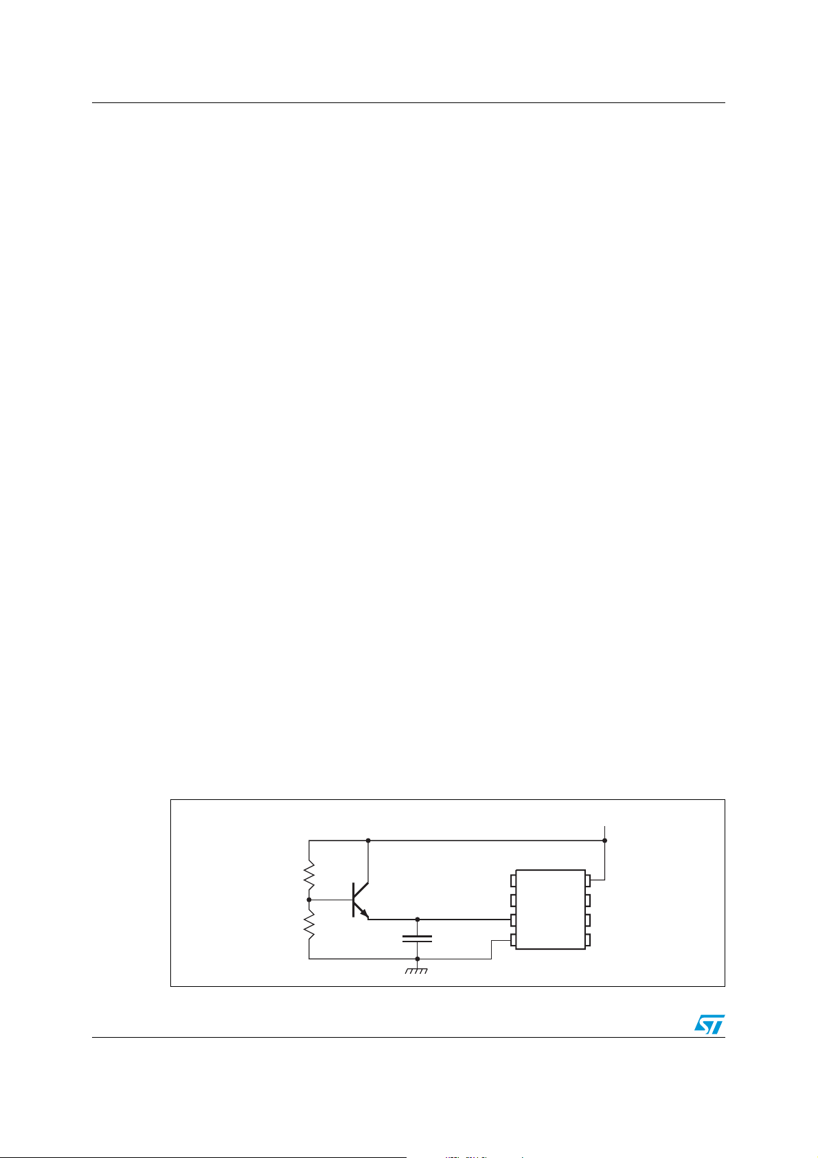
Figure 1. External connections to the M41T56
R1
V
BASE
R2
C
2/6 Doc ID 5226 Rev 2
×=
1.0V
------------
Δt
M41T56
V
V
BAT
V
SS
+5V
CC
AI02481
Page 3

AN922
Calculating the values of the circuit components for the M41T00, M41T11, and M41T81
The minimum operating voltage for these devices is 2.0 V, with a typical V
V
– VF (diode).
CC
Therefore, the typical delta voltage swing across the capacitor is:
voltage of
BAT
ΔVVCCVF– VCCmin–=
where V
is approximately 0.5 V. Therefore:
F
ΔV5.0V0.5V– 2.0V–=
ΔV2.5V=
Since the battery current (I
the duration of “power-out time” can be calculated using the formula:
) is limited to maximum value of 1.0 µA, the capacitance and
BAT
CΔV
I
------------=
Δt
where I = 1.0 µA, ΔV = 2.5 V, C = capacitance in Farads, and Δt = “power-out time” in
seconds.
Using a 100,000 µF capacitor, for example, the equation would be:
2.5V
1.0μA0.1F
Solving for Δt, the maximum power down time is about 250,000 seconds. This is 69.4 hours,
or 2.9 days.
×=
------------
Δt
Doc ID 5226 Rev 2 3/6
Page 4

AN922
Calculating the values of the circuit components for the M41ST84W and M41T94
The minimum operating voltage for these devices is 2.5 V, with a typical V
V
– VF (diode).
CC
Therefore, the typical delta voltage swing across the capacitor is:
voltage of
BAT
ΔVVCCVF– VCCmin–=
where V
is approximately 0.5 V. Therefore:
F
ΔV5.0V0.5V– 2.5V–=
ΔV2.0V=
Since the battery current (I
and the duration of “power-out time” can be calculated using the formula:
) is limited to the maximum value of 500 nA, the capacitance
BAT
CΔV
I
------------=
Δt
where I = 500 nA, ΔV = 2.0 V, C = capacitance in Farads, and Δt = “power-out time” in
seconds. Using a 100,000 µF capacitor, for example, the equation would be:
2.0V
500nA 0.1F
Solving for Δt, the maximum power down time is about 400,000 seconds. This is 111.1
hours, or 4.63 days.
Figure 2. External connections to the M41T00, M41T11, M41T81, M41T94, and
M41ST84W (16-pin)
×=
------------
Δt
+5V
VF~0.5V
C
V
V
BAT
SS
V
CC
AI02854
4/6 Doc ID 5226 Rev 2
Page 5

AN922 Revision history
Revision history
Table 1. Document revision history
Date Revision Changes
Feb-2002 1 Initial release.
19-Sep-2011 2
Product updates; minor textual updates; revised document
presentation.
Doc ID 5226 Rev 2 5/6
Page 6

AN922
Please Read Carefully:
Information in this document is provided solely in connection with ST products. STMicroelectronics NV and its subsidiaries (“ST”) reserve the
right to make changes, corrections, modifications or improvements, to this document, and the products and services described herein at any
time, without notice.
All ST products are sold pursuant to ST’s terms and conditions of sale.
Purchasers are solely responsible for the choice, selection and use of the ST products and services described herein, and ST assumes no
liability whatsoever relating to the choice, selection or use of the ST products and services described herein.
No license, express or implied, by estoppel or otherwise, to any intellectual property rights is granted under this document. If any part of this
document refers to any third party products or services it shall not be deemed a license grant by ST for the use of such third party products
or services, or any intellectual property contained therein or considered as a warranty covering the use in any manner whatsoever of such
third party products or services or any intellectual property contained therein.
UNLESS OTHERWISE SET FORTH IN ST’S TERMS AND CONDITIONS OF SALE ST DISCLAIMS ANY EXPRESS OR IMPLIED
WARRANTY WITH RESPECT TO THE USE AND/OR SALE OF ST PRODUCTS INCLUDING WITHOUT LIMITATION IMPLIED
WARRANTIES OF MERCHANTABILITY, FITNESS FOR A PARTICULAR PURPOSE (AND THEIR EQUIVALENTS UNDER THE LAWS
OF ANY JURISDICTION), OR INFRINGEMENT OF ANY PATENT, COPYRIGHT OR OTHER INTELLECTUAL PROPERTY RIGHT.
UNLESS EXPRESSLY APPROVED IN WRITING BY TWO AUTHORIZED ST REPRESENTATIVES, ST PRODUCTS ARE NOT
RECOMMENDED, AUTHORIZED OR WARRANTED FOR USE IN MILITARY, AIR CRAFT, SPACE, LIFE SAVING, OR LIFE SUSTAINING
APPLICATIONS, NOR IN PRODUCTS OR SYSTEMS WHERE FAILURE OR MALFUNCTION MAY RESULT IN PERSONAL INJURY,
DEATH, OR SEVERE PROPERTY OR ENVIRONMENTAL DAMAGE. ST PRODUCTS WHICH ARE NOT SPECIFIED AS "AUTOMOTIVE
GRADE" MAY ONLY BE USED IN AUTOMOTIVE APPLICATIONS AT USER’S OWN RISK.
Resale of ST products with provisions different from the statements and/or technical features set forth in this document shall immediately void
any warranty granted by ST for the ST product or service described herein and shall not create or extend in any manner whatsoever, any
liability of ST.
ST and the ST logo are trademarks or registered trademarks of ST in various countries.
Information in this document supersedes and replaces all information previously supplied.
The ST logo is a registered trademark of STMicroelectronics. All other names are the property of their respective owners.
© 2011 STMicroelectronics - All rights reserved
STMicroelectronics group of companies
Australia - Belgium - Brazil - Canada - China - Czech Republic - Finland - France - Germany - Hong Kong - India - Israel - Italy - Japan -
Malaysia - Malta - Morocco - Philippines - Singapore - Spain - Sweden - Switzerland - United Kingdom - United States of America
www.st.com
6/6 Doc ID 5226 Rev 2
 Loading...