

Page 1

AN910
APPLICATION NOTE
ST7 AND ST9 PERFORMANCE BENCHMARKING
INTRODUCTION
STMicroelectronics has developed a set of test routines related to 8-bit and low-end 16-bit
microcontroller applications to evaluate computing performance and interrupt processing
performance of microcontroller cores. These routines have been implemented on ST7 and
ST9 Microcontroller Units (MCUs) as well as several MCUs available on the market.
The routines have been written in assembler language to optimize their implementation and
focus on core performance, without being dependent upon compiler code transformation.
For each test, the two parameters of interest are execution time and code size. Timings have
been either measured whenever possible, or theoretically calculated when there was no other
alternative. In most cases, programs have really run and execution times have actually been
measured, so that assembly sources should not contain implementation errors and results can
be considered as correct and reliable.
The results of this study point out the capability of the ST9+ to compete with 16-bit MCUs on
8-bit and low-end 16-bit applications and confirms its position of high-end 8/16-bit MCU. It
also confirms the ST7 as an outstanding 8-bit MCU.
The first four sections provide synthetical information:
1. Overview of the Test Routines on page 2
2. Overview of the MCU cores on page 3
3. Benchmark results on page 4
4. Result analysis on page 11
More detailed information is provided in the appendixes:
5. Description of MCU work environments on page 17
6. Complete numerical results on page 21
7. MCU Core architecture analysis on page 25
8. Description of the test routines on page 43
9. Measurement proceeding and calculation on page 46
Rev. 2.0
AN910/1104 1/51
1
Page 2
ST7 AND ST9 PERFORMANCE BENCHMARKING
1 OVERVIEW OF THE TEST ROUTINES
Eleven different test routines have been implemented in assembler language.
The first ten routines are oriented at measuring core computing performance. They are
based on known algorithms and represent currently used operations in 8-bit and low-end 16bit applications. They mix bit, 8-bit and 16-bit operations as many applications do.
This set of tests is described in Table 1.
Table 1. Test routine overview
Abbreviated name Full name Description Features stressed
sieve Eratosthenes sieve
acker(m,n)
string String search
char Character search search a byte in a 40-byte array
bubble(n)
blkmov(n)
convert Block translation
16mul 16-bit integer multiplication
shright 16-bit value right shift
bitsrt Bit manipulation
1) The couple of values used are (m,n)=(3,5) and (m,n)=(3,6)
2) The values used are n=10 (words) and n=600 (words)
3) The values used are n=64 (bytes) and n=512 (bytes)
1)
2)
3)
Ackermann function
Bubble sort
Block move
find prime numbers ≥ 3 out of
8189 elements
make recursive function calls
number of calls depending upon
two parameters (m,n)
search a 16-byte string in a 128character array
sort of a one-dimension array of
n 16-bit integers
move a n-byte block from a
place in memory to another
translate a 121-byte block in a
different format
multiplication of two unsigned
words giving a 32-bit result
shift a 16-bit value five places to
the right
set, reset, and test of 3 bits in a
128-bit array
16-bit data computation
bit manipulation
function calls
stack use
8-bit data block manipulation
string manipulation
8-bit data manipulation
char manipulation
16-bit data manipulation
integer manipulation
8-bit data block manipulation
block move
8-bit data manipulation
use of a lookup table
16-bit data computation
integer manipulation
16-bit data manipulation
bit manipulation
bit computation
bit and 8-bit data manipulation
Another test routine handling a timer interrupt has been used to measure core interrupt
processing performance:
Abbreviated name Full name Description Features stressed
standard timer input capture or/
interrupt Timer interrupt
and output compare interrupt
service routine
interrupt processing
A more precise description of the test routines is available in section 8.
2/51
2
Page 3
ST7 AND ST9 PERFORMANCE BENCHMARKING
2 OVERVIEW OF THE MCU CORES
The set of MCUs evaluated is composed of various 8-bit, 8/16-bit, and 16-bit
microcontrollers with accumulator, register file or mixed architectures.
Table 2 is an overview of the MCU cores.
Table 2. MCU cores overview
MCU name Architecture Short core description Freq
80C51XA
PHILIPS
68HC16
MOTOROLA
68HC12
MOTOROLA
ST9+
STMicroelectronics
ST9
STMicroelectronics
H8/300
HITACHI
68HC11
MOTOROLA
68HC08
MOTOROLA
ST7
STMicroelectronics
80C51
INTEL, PHILIPS...
KS88
SAMSUNG
78K0
NEC
1) As the goal is to obtain the best of each MCU core, the maximum internal frequency (Freq) available, for each MCU, on
development board has been used (unless other specified). Note that results are directly proportional to this frequency.
16-bit;
register file
16-bit;
two
accumulators
16-bit;
two
accumulators
8/16-bit;
register file
8/16-bit;
register file
8/16-bit;
register file
8-bit;
two
accumulators
8-bit;
accumulator
8-bit;
accumulator
8-bit; register file
and accumulator
8-bit;
register file
8-bit; register file
and accumulator
eXtended Architecture (XA) of 80C51’s - upward compatible
8/16-bit register bus - 16-bit data/program memory buses
register file programming model with sixteen 16-bit banked registers
core architecture superset of 68HC11’s - upward compatible
accumulator programming model with two 16-bit accumulators, and
three 16-bit index registers (all with 4-bit extensions)
instruction set is superset of 68HC11’s - upward compatible
programming model identical to 68HC11’s
evolution of the ST9
enhanced clock speed, instruction cycle time
enlarged memory space
8/16-bit architecture; 8-bit register bus - 16-bit memory bus
register file programming model with 14 groups of sixteen 8-bit
registers, useable as 16-bit registers
modular paged registers for access to peripheral registers
RISC-like architecture and instruction set
register file programming model with sixteen 8-bit registers
market standard 8-bit MCU
accumulator programming model with two 8-bit accumulators or
one 16-bit accumulator, and two 16-bit index registers
superset of the 68HC05 - upward compatible
enhanced performance and instruction set
accumulator programming model with one 8-bit accumulator, and
one 16-bit index register
upward compatible with the 68HC05
accumulator programming model with one 8-bit accumulator, and
two 8-bit index registers
mixed accumulator and register file programming model with four
banks of eight 8-bit registers (include accumulator), and a 16-bit
data pointer
core architecture superset of SUPER8’s; 8-bit register bus
register file programming model with 192 8-bit prime data registers,
and two register sets with system/peripheral/data registers
mixed accumulator and register file programming model with four
banks of eight 8-bit or four 16-bit registers (include accumulator)
1)
20 MHz
16 MHz
8 MHz
25 MHz
12 MHz
10 MHz
4 MHz
8 MHz
4 MHz
8 MHz
20 MHz
8 MHz
10 MHz
A description of the MCU work environments is available in section 5.
3/51
Page 4

ST7 AND ST9 PERFORMANCE BENCHMARKING
3 BENCHMARK RESULTS
3.1 CORE COMPUTING PERFORMANCE
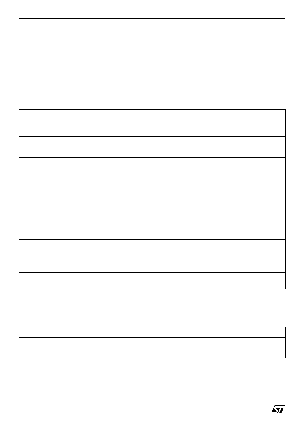
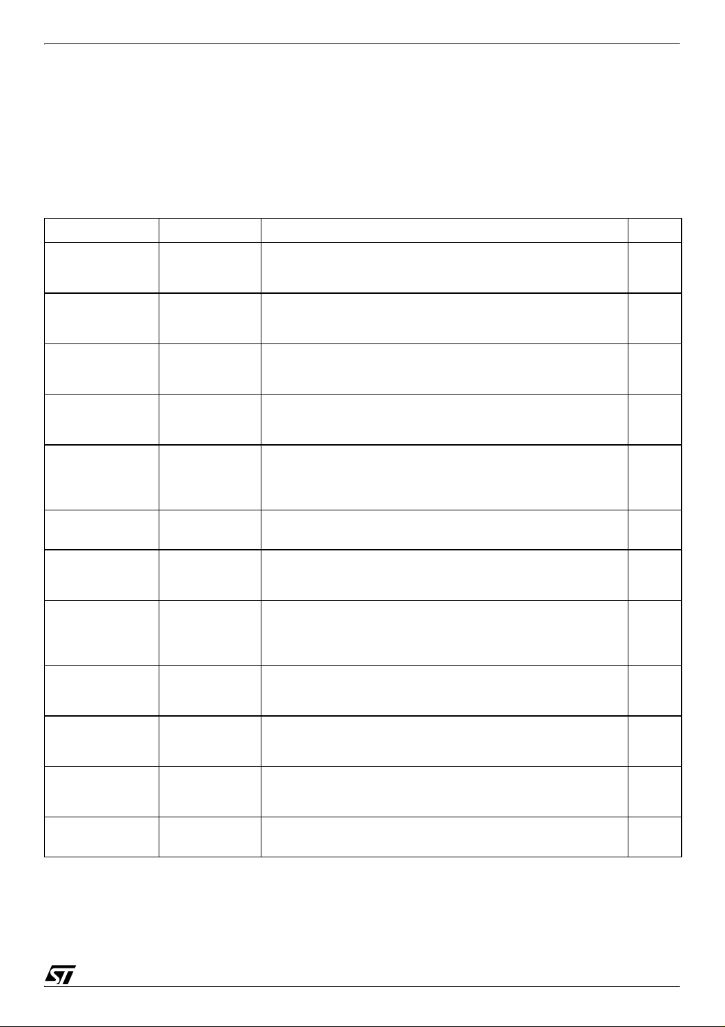
The two following charts show benchmark results for computing performance. Execution time
and code size are presented as global ratios taken the ST9+ as reference.
Preliminary ratios have been calculated for each test. Using those results, a global execution
time ratio and a global code size ratio have been calculated as an average of all ratios. As all
the tests could not have been implemented on all MCUs (
considerations<Italic end>), one or two different results are presented for each MCU. The
first one, available for all the MCUs, has been calculated with the reduced set of tests
performed on all the MCUs. The second one, only available for some MCUs, has been
calculated with the full set of tests.
Refer to section 6 for complete results. Refer to section 9 for measurement proceeding and
calculation description.
see <Italic>9.2.2 Memory
Figure 1. presents execution time ratios and Figure 2. shows code size ratios.
Notes: The reduced set of tests is composed of:
string, char, bubble(10 words), blkmov(64 bytes), convert, 16mul, shright, bitrst
The full set of tests is composed of:
string, char, bubble(10 words), blkmov(64 bytes), convert, 16mul, shright, bitrst,
sieve, acker(3,5), acker(3,6), bubble(600 words), blkmov(512 bytes)
The 80C51 results are preliminary results. They may change in later versions.
4/51
Page 5
ST7 AND ST9 PERFORMANCE BENCHMARKING
best performance
8-bit MCUs 16-bit MCUs8/16-bit MCUs
Figure 1. Computing performance global execution time ratios (ST9+ as reference)
5/51
Page 6
ST7 AND ST9 PERFORMANCE BENCHMARKING
best density
8-bit MCUs 16-bit MCUs8/16-bit MCUs
6/51
Figure 2. Computing performance global code size ratios (ST9+ as reference)
Page 7

ST7 AND ST9 PERFORMANCE BENCHMARKING
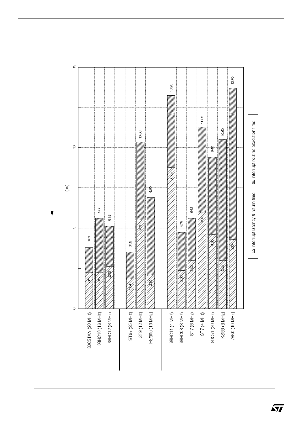
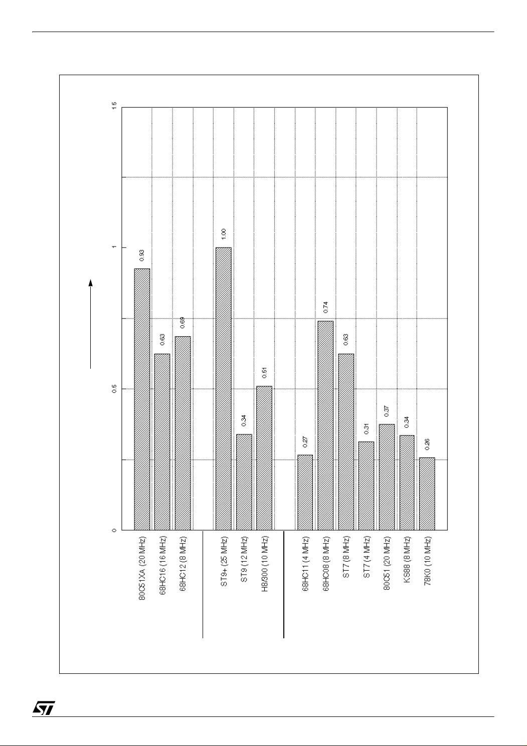
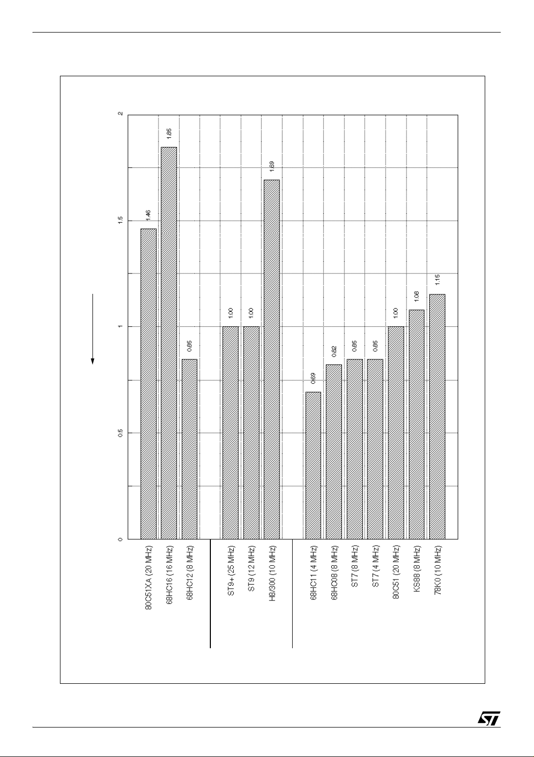
3.2 CORE INTERRUPT PROCESSING PERFORMANCE
The three following charts show benchmark results for interrupt processing performance.
Execution time results are presented as time values (in microseconds), and also as ratios
taken the ST9+ as reference. Code size results are presented as ratios taken the ST9+ as
reference.
Refer to section 6 for complete results and details on calculation.
Figure 3. presents execution time results in microseconds, showing interrupt latency & return
time.
Figure 4. presents execution time ratios, and Figure 5. presents code size ratios.
7/51
Page 8
ST7 AND ST9 PERFORMANCE BENCHMARKING
best performance
8-bit MCUs 16-bit MCUs8/16-bit MCUs
8/51
Figure 3. Interrupt processing performance execution time values
Page 9
ST7 AND ST9 PERFORMANCE BENCHMARKING
best performance
8-bit MCUs 16-bit MCUs8/16-bit MCUs
Figure 4. Interrupt processing performance execution time ratios (ST9+ as reference)
9/51
Page 10
ST7 AND ST9 PERFORMANCE BENCHMARKING
best density
8-bit MCUs 16-bit MCUs8/16-bit MCUs
10/51
Figure 5. Interrupt processing performance code size ratios (ST9+ as reference)
Page 11

ST7 AND ST9 PERFORMANCE BENCHMARKING
4 RESULT ANALYSIS
This section is an analysis of computing performance and interrupt processing
performance results (for execution time and code size). Based on core architecture analysis
section 7), two comparisons are presented, pointing out the strong and weak points of
(see
each MCU. The first concerns the high-end to medium-end MCUs versus ST9+. The
second concerns the medium-end to low-end MCUs versus ST7.
4.1 PRELIMINARY REMARK
Results show that the two different ratios, for execution time and code size, calculated with full
and reduced sets of tests, are in fact not very different. In most cases, the classification of the
MCUs is kept. Thus we can consider that the reduced set is sufficient to make the MCU
core comparison.
4.2 HIGH-END TO MEDIUM-END MCU ANALYSIS VERSUS ST9+
The Table 3 presents the strong and the weak points for high-end to medium-end MCUs,
compared to the ST9+ MCU.
Notes: ICT means Instruction Cycle Time and IL means Instruction Length.
Refer to paragraph <Italic>7.2.2 Average ICT/CPI and IL<Italic end> for details on
calculation.
Refer to paragraph <Italic>7.3.4 ST9+ MCU core<Italic end> to see the main characteristics of
the ST9+ MCU core.
4.2.1 Computing performance results
Regarding speed, the ST9+ MCU ranks at the top of 8/16-bit MCUs. This new version of the
ST9 has been improved on several points, including clock per instruction and clock speed.
These enhancements have considerably reduced its instruction cycle time. A large and
powerful register file organized in groups allow the ST9+ to perform strong computation
(with many registers), have an easy access to peripheral and i/o port registers (with paged
registers), and manage multitasking (with register group pointers). Addressing modes like
register pair, register indirect with pre/post-increment, and indexed give the ST9+ the ability to
perform 16-bit data computation and manipulation, easily manipulate tables and move
blocks. A new memory management unit enlarges the memory space up to 4 Mbytes. New
instructions have been added to handle this new space and improve the C-language
support.
11/51
Page 12

ST7 AND ST9 PERFORMANCE BENCHMARKING
Concerning code efficiency, the position of the ST9+ MCU is also among the best MCUs.
The 16-bit MCUs are only a little better, although favoured by their true 16-bit computing and
data manipulation instructions. In the 8/16-bit MCUs, the H8/300 takes a little advantage due
to its special block move instruction. But all 8-bit MCUs, even with shorter instruction lengths,
have longer code size results.
4.2.2 Interrupt processing performance results
Regarding speed, the ST9+ MCU ranks at the first position. The value chart shows that it
has the shortest interrupt latency but also an interrupt routine execution time which is
among the best. These results show that its interruption management and instruction cycle
time have been considerably enhanced. The register groups bring in addition fast context
switching capabilities.
Some 8-bit MCUs, such as the 68HC08, work quite well in this test. But their performance
must be moderated because such MCUs can manage only one interrupt at the time and so
cast off a complex arbitration phase. The interrupt management of the ST9+ is one of the
more advanced, allowing nested interrupts with full software programmable priorities
and program priority level control.
Code efficiency results for interrupt processing performance are not really significant. The
code represents only a very small part of an entire interrupt service routine, and so no
conclusion can be made.
4.2.3 Conclusion
Global results and all its characteristics allow the ST9+ to compete with the true 16-bit
MCUs on 8-bit and low-end 16-bit applications, and confirm its position of high-end 8/16-bit
MCU.
12/51
Page 13
ST7 AND ST9 PERFORMANCE BENCHMARKING
Table 3. High-end to low-end MCU strong and weak points
MCU Strong points Weak points
7-byte prefetch queue
predecoding
16-bit datapath
600 ns 8x8 multiplication
250 to 300 ns
indirect with 8/16 offset or
auto-increment
compare & branch like
decrement & branch like
memory-to-memory moves
context switching capabilities
up to 16 Mbytes
nested mode
4-bit program priority register
programmable priority levels
3-stage prefetch queue
predecoding
16-bit datapath
625 ns 8x8 multiplication
375 to 440 ns
post-modified indexed
with 8-bitoffset
memory-to-memory moves
context switching capabilities
up to 1 Mbyte
up to 16 Mbytes with memory
expansion module
nested mode
3-bit program priority register
programmable priority levels
2-stage prefetch queue
predecoding
20-bit datapath
375 ns 8x8 multiplication
375 to 500 ns
auto-incr/decrement indexed
accumulator offset indexed
memory-to-memory moves
incr/decrement & branch like
test & branch like
up to 4 Mbytes with memory
expansion module
risc-like encoding
2 to 3 bytes
register indirect, 16-bit offset
or pre/post-increment
block moves
address alignment:
lacking addr. modes:
address alignment:
instruction lengths:
lacking addr. modes:
lacking instructions:
multitasking:
interrupt processing:
instruction processing:
medium 8/16-bit ALU:
medium average ICT:
lacking instructions:
multitasking:
memory space:
interrupt processing:
80C51XA
(20 MHz)
68HC16
(16 MHz)
68HC12
(8 MHz)
H8/300
(10 MHz)
instruction processing:
fast 8/16-bit ALU:
short average ICT:
special addr. modes:
special instructions:
multitasking:
large memory space:
interrupt processing:
instruction processing:
fast 8/16/32-bit ALU:
short average ICT:
special addr. modes:
special instructions:
multitasking:
large memory space:
interrupt processing:
instruction processing:
fast 8/16-bit ALU:
short average ICT:
special addr. modes:
special instructions:
large memory space:
instruction encoding:
short average IL:
special addr. modes:
special instructions:
even jump/branch address
even word operand address
NOP instructions in assembly
code
no indexed addressing
performance penalty if odd
word operand addresses
only even
no direct addressing
index register manipulation
compare & branch like
decrement & branch like
need memory expansion
module
one interrupt at a time
recommended
no program priority register
hardware fixed priorities
standard (no prefetch)
1400 ns 8x8 multiplication
500 to 600 ns
16-bit shifts/rotations
compare & branch like
decrement & branch like
no special capabilities
64 kbytes
one interrupt at a time
recommended
no program priority register
hardware fixed priorities
13/51
Page 14
ST7 AND ST9 PERFORMANCE BENCHMARKING
Table 3. High-end to low-end MCU strong and weak points (cont’d)
MCU Strong points Weak points
instruction processing:
medium 8/16-bit ALU:
long average ICT:
lacking instructions:
68HC11
(4 MHz)
68HC08
(8 MHz)
instruction processing:
fast 8-bit ALU:
special addr. modes:
special instructions:
large memory space:
1-byte prefetch queue
8-bit datapath
625 ns 8x8 multiplication
indexed with 8-bit offset or
post-increment
memory-to-memory moves
compare & branch like
decrement & branch like
up to 4 Mbytes with memory
expansion module
multitasking:
memory space:
interrupt processing:
medium average ICT:
lacking addr. modes:
multitasking:
interrupt processing:
standard (no prefetch)
2500 ns 8x8 multiplication
1500 to 1750 ns
compare & branch like
decrement & branch like
no special capabilities
64 kbytes
one interrupt at a time
recommended
no program priority register
hardware fixed priorities
500 to 625 ns
no indirect addressing
no special capabilities
one interrupt at a time
recommended
no program priority register
hardware fixed priorities
14/51
Page 15

ST7 AND ST9 PERFORMANCE BENCHMARKING
4.3 MEDIUM-END TO LOW-END MCU ANALYSIS VERSUS ST7
The Table 4 presents the strong and the weak points for medium-end to low-end MCUs,
compared to the ST7 MCU.
Notes: ICT means Instruction Cycle Time and IL means Instruction Length.
Refer to paragraph <Italic>7.2.2 Average ICT/CPI and IL<Italic end> for details on
calculation.
Refer to paragraph <Italic>7.3.9 ST7 MCU core<Italic end> to see the main characteristics of
the ST7 MCU core.
4.3.1 Computing performance results
Regarding speed, the ST7 MCU takes the second position just below the newly arrived
68HC08. With no prefetch mechanism, it comes even so ahead of all the other MCUs. A short
clock per instruction added to a standard frequency explains its short instruction cycle time
and its advantageous position. The two index registers and the indirect addressing mode
allow the ST7 to easily perform data manipulation like table manipulation and block move.
A direct addressing mode in a 256-byte zero page give a rapid access to important data
and peripheral registers.
Concerning code efficiency, the ST7 MCU ranks among the 8-bit MCUs, very closely above
the 68HC08. A standard instruction length explains its average position.
4.3.2 Interrupt processing performance results
Regarding speed, the ST7 MCU ranks very close to the 68HC08. A longer instruction cycle
time explains this tiny gap. The strong point of its interrupt management is the automatic
stacking of the cpu state, accumulator and index register. This process eliminates software
stacking, and so saves time and space.
Code efficiency results for interrupt processing performance are not really significant. The
code represents only a very small part of an entire interrupt service routine, and so no
conclusion can be made.
4.3.3 Conclusion
Global results and all its characteristics confirm the ST7 as an outstanding 8-bit MCU.
15/51
Page 16
ST7 AND ST9 PERFORMANCE BENCHMARKING
Table 4. Medium-end to low-end MCU strong and weak points
MCU Strong points Weak points
medium 8/16-bit ALU:
68HC11
(4 MHz)
68HC08
(8 MHz)
80C51
(20 MHz)
KS88
(8 MHz)
78K0
(10 MHz)
instruction processing:
fast 8-bit ALU:
short average ICT:
special addr. modes:
special instructions:
large memory space:
short average IL:
special addr. modes:
special instructions:
multitasking:
special addr. modes:
special instructions:
multitasking:
interrupt processing:
special addr. modes:
special instructions:
multitasking:
1-byte prefetch queue
8-bit datapath
625 ns 8x8 multiplication
500 to 625 ns
indexed with 8-bit offset or
post-increment
compare & branch like
decrement & branch like
memory-to-memory moves
up to 4 Mbytes with memory
expansion module
1 to 2 bytes
register indirect
stack pointer relative
compare & branch like
decrement & branch like
bit test & bit clear & jump
memory-to-memory moves
context switching capabilities
register pair
indirect register/address
indexed (short/long)
compare & increment &
branch like
decrement & branch like
context switching capabilities
nested mode
level priority control register
register indirect
stack pointer relative
indexed with 8-bit offset
decrement & branch like
context switching capabilities
long average ICT:
lacking instructions:
multitasking:
lacking addr. modes:
multitasking:
slow 8-bit ALU:
long average ICT:
slow 8-bit ALU:
long average ICT:
data memory location:
mixed architecture:
slow 8-bit ALU:
long average ICT:
2500 ns 8x8 multiplication
1500 to 1750 ns
compare & branch like
decrement & branch like
no special capabilities
no indirect addressing
no special capabilities
2400 ns 8x8 multiplication
900 to 1000 ns
3000 ns 8x8 multiplication
1250 to 1500 ns
off-chip only
only accumulator oriented
3200 ns 8x8 multiplication
1400 to 1600 ns
16/51
Page 17

ST7 AND ST9 PERFORMANCE BENCHMARKING
5 DESCRIPTION OF MCU WORK ENVIRONMENTS
This section is a short description of the work environment, with the tools used (hardware and
software tools), for each MCU during the benchmarks.
5.1 80C51XA MCU TOOLS
P51XAG35 chip
Hardware tools
Software tools
5.2 68HC16 MCU TOOLS
Hardware tools
Software tools
P51XADB/E development board/emulator
Note that no external RAM was available on the development board.
A Microsoft Windows based integrated development environment have been elaborated upon by
Macraigor Systems Incorporated. The interesting tools for the benchmarks were a standard
editor, an XA absolute macro assembler, and an emulator interface/debugger.
MC68HC16Z1 chip
M68HC16Z1EVB evaluation board
Jumpers are set to configure the board.
Note that, to access the I/O pin used for execution time measuring, a context switch is needed
and add to each test routine 6 bytes and 375 ns. This length and time have been subtracted from
measured results, in order not to disadvantage this MCU. If they are taken into account, the
computing performance results are just a little worse (1.40) but code efficiency decreases down
to 1.45.
Note that the external RAM of the evaluation board needs wait states and so was not use.
MASM16 (DOS environment) is an integrated environment for writing, editing assembling and
debugging source code. It also allows to set the assembler options which are:
masm -I'name'.lst -o'name'.o -a -b 'name'.asm >_masm16.err
EVB16 is a DOS debugger for 68HC16Z1EVB.
5.3 68HC12 MCU TOOLS
MC68HC812A4 chip
Hardware tools
Software tools
M68HC12A4EVB evaluation board
Jumpers have been left as configured in factory.
Note that the external RAM of the evaluation board needs wait states and so was not use.
The development of the routines is performed within an Integrated Development Environment
(IDE)
manager (MCU project), a macro-assembler (MCU asm), and a Motorola S-record generator
(hex). The compilation options are:
A communications program is then necessary to connect the PC to the evaluation board through
a RS232 serial link. We have used PROCOMM PLUS for Windows, but any other
communications program can suit the link to the Evaluation Board and its D-Bug12 monitor/
debugger program, resident in external EPROM.
Note that the ‘TBNE’, ‘TBEQ’, ‘DBNE’, ‘DBEQ’, ‘IBNE’, and ‘IBEQ’ instructions were not usable
without problems with the board used.
: Motorola MCU software. In a Windows environment, this software brings a project
masm -y -W3 -I'name'.lst -a -o'name'.o 'name'.asm
hex -F'name'.hex 'name'.o
17/51
Page 18

ST7 AND ST9 PERFORMANCE BENCHMARKING
5.4 ST9+ MCU TOOLS
ST90R192 chip
Hardware tools
Software tools
5.5 ST9 MCU TOOLS
Circuit Real Time Emulation System ST9+ HDS2 (Hardware Development System 2)
The PLL clock has been used (see configuration in assembly codes)
The GNU C Toolchain (GCC9) for the ST9+ is used to assemble the code sources (in assembler
language). The command line with its options is:
gcc9 -v -g -c -o 'name'.o 'name'.st9
Then it is linked with the linker LD9:
ld9 -I -i -m -Tdata 0x10000300 -o 'name'.u 'name'.o
To debug the program, the Windows Debugger WGDB9xxx for ST9+ is used together with the
emulator. Here, the configuration file hardware.gdb is the following one:
clear_map
map 0x000000 32 sw
map 0x008000 16 sr
Hardware tools
Software tools
ST90R50 chip
Circuit Real Time Emulation System ST9 HDS2 (Hardware Development System 2)
The GNU C Toolchain for ST9 is used. The options are the following ones:
The Windows Debugger WGDB9xxx is used with the configuration file hardware.gdb :
5.6 H8/300 MCU TOOLS
H8/330 chip
LEV8330 evaluation board
Default jumpers’ settings have been kept.
Hardware tools
Software tools
Note that the code was placed on external memory (the size of internal RAM is limited to 512
bytes). As the access to external memory is 3 times longer than the access to internal memory,
the measured execution time results have been corrected. For each test, a value, equals to
(200ns x number of bytes executed), has been subtracted (200ns for each byte of code).
Actually, only the instruction fetch was wrong, and it lasted 300ns instead of 100ns for each byte.
The Eurodesc H-series Interface Software (INTFC3) allows the user to communicate with the
Hitachi's Executive Monitor System (EMS) located on the development board. It uses a DOS
environment.
gcc9 -v -g -c -o 'name'.o 'name'.st9
ld9 -I -i -m -Tdata 0x10000300 -o 'name'.u 'name'.o
bankswitch off
pd_signal used
sdb sr ea 3<<2
sdb sr fc 08
sdb sr fd 08
sdb sr fe 00
# Mapping of memory
map p:0x0000 0x7FFF SR
map D:0x0000 0x7FFF SW
18/51
Page 19

5.7 68HC11 MCU TOOLS
MC68HC11A8 chip
MC68HC11A8EVM evaluation board
Hardware tools
Software tools
Note that the internal chip frequency on evaluation board was 2 MHz, but as 4 MHz versions are
available, this frequency was used for results (execution time values have been divided by 2).
Note that it was not possible to emulate external RAM.
The integrated assembler IASM11 (DOS environment) allows to blend an editor and a cross
assembler into one single environment.
A DOS environment is used to debug programs.
5.8 68HC08 MCU TOOLS
MC68HC708XL36 chip
Hardware tools
Software tools
EML08XL36 emulator module plugged in the M68MMEVS05 modular evaluation system
(platform board for EML08XL36)
Jumpers configure both.
Rapid, a software development tool in a DOS environment allows to execute all the operations.
It consists of a configuration program (Rinstall) and a cross assembler (CASM). Rinstall contains
a serie of data entry screens. Only CASM and the MMEV08X DOS debugger were configured
as follows:
Note that the assembler does not seem to manage the zero page addressing mode. Thus, the
results have been modified to take this addressing mode into account. Without zero page
addressing mode, the execution time result changes to 0.61 and the code size result increases
up to 1.43.
ST7 AND ST9 PERFORMANCE BENCHMARKING
• Cross assembler configuration: “CASM assembler” entry screen
Name and fully path: 'path_of_CASM08.exe'
Primary options: S L D
Secondary options: S L D I
• Debugger configuration: “Debugger” entry screen
Fully path: 'path_of_MMEVS08.exe'
Options: -B
5.9 ST7 MCU TOOLS
ST7275 chip
ST7 HDS (Hardware Development System) emulator with ST7275 DBE (Dedicated Board
Hardware tools
Software tools
Emulator)
Note that measures have been made with a 4 MHz MCU, but as 8 MHz versions exist, two values
are presented with the two frequencies (for the 8 MHz version, execution time values have been
divided by 2).
The toolchain used for the ST7 includes a meta-assembler (ASM), a generic linker (LYN), and a
generic formatter (OBSEND). These software tools are used with the following options
The Windows environment is used by the debugger: Windows Debugger WGDB7.
:
asm -sym -li 'name'
lyn 'name'
asm 'name' -fi = 'name'.map
obsend 'name', f, 'name'.s19, srec
19/51
Page 20

ST7 AND ST9 PERFORMANCE BENCHMARKING
5.10 80C51 MCU TOOLS
P80C32GBPN chip
MicroTek EASYPACK 8051 serial emulator
Hardware tools
Software tools IAR 8051 assembler
5.11 KS88 MCU TOOLS
Hardware tools
Software tools
Note that the internal chip frequency on evaluation board was 12 MHz, but as 20 MHz versions
are available, this frequency was used for results (execution time values have been divided by
20/12).
KS880504 and KS880116 chips
SMDS II in-circuit emulator (Samsung Microcontroller Development System 2) with target boards
TB880504A and TB880116A
A function generator has been used to reach the 8 MHz frequency. It has been connected to the
Personality Board in the SMDS2 emulator after having selected the EXTRA clock source with the
switches in the front panel.
Note that this MCU do not own any internal RAM - register file space excepted. It was also
impossible to emulate external memory. Tests have been performed using register file only.
Everything is done from the SMDS operating program software (DOS environment). SAMA
(Samsung Assembler) is used to assemble the programs with the following command line and
options:
SAMA.EXE %S /K /LST
Then, the program is loaded to SMDS2 memory (emulation memory) and a work file is made ([M]
key). The debugging screen is accessed with the [D] key.
5.12 78K0 MCU TOOLS
µPD78P014 chip
Hardware tools
Software tools
78K0 starter kit
Note that it was not possible to emulate external RAM.
The µPD78P014 toolchain consists of a Micro Series assembler (A78000) and a Micro Series
generic linker (XLINK). The command lines are as follows:
The file bench.xcl extends the length of xlink command line. The extra options included in
bench.xcl are:
The 78K0 starter kit has a DOS environment.
A78000 'name'.asm 'name'.lst
xlink 'name' -o 'name'.o -f bench.xcl
-c78000
-Fnec
-Z(CODE)INTVEC=8000
-Z(CODE)CODE=8080
-Z(DATA)DATA=FB00
-Z(DATA)WRKSEG,SHORTAD=FE20-FEDF
-Z(BIT)BITVARS=0
-Y2
20/51
Page 21

ST7 AND ST9 PERFORMANCE BENCHMARKING
6 COMPLETE NUMERICAL RESULTS
Here are the tables with the complete numerical results.
6.1 CORE COMPUTING PERFORMANCE
The first two tables (Table 5 and Table 6) concern execution time with the values measured
in milliseconds and the ratios calculated with ST9+ MCU as reference. The next two tables
Table 7 and Table 8) concern code size with the values measured in bytes and the ratios
(
calculated with ST9+ MCU as reference. The last two tables (Table 9 and Table 10) present
global execution time ratios and global code size ratios with reduced and full set of tests.
Refer to section 9 for measurement proceeding and calculation description.
Notes: The reduced set of tests includes string, char, bubble(10 words), blkmov(64 bytes),
convert, 16mul, shright, bitrst tests. They are in boldface characters.
Numbers with parenthesis have been judged out of range and have not been taken
into account. In fact, it means that this specific test was absolutely unadapted to this
specific MCU. Only some tests, which are not include in the reduced set, are
concerned.
Legend:
6.2 CORE INTERRUPT PROCESSING PERFORMANCE
▲ x.xx
▼ x.xx
best results
worst results
Table 11 concerns execution time with the values measured in microseconds, showing
interrupt latency & return time, the total time, and the ratios calculated with ST9+ MCU as
reference.
Table 12 concerns code size with the values measured in bytes and the ratios
calculated with ST9+ MCU as reference.
The execution time has only been calculated theoretically with the assembly code, like
computing performance theoretical execution time (
see <Italic>9.1.1 Execution time
measure<Italic end>). The result is the sum of the interrupt latency (execution time of the
longest instruction and interrupt entry time) and the execution time of the interrupt service
routine. The code size has been calculated with the assembly code.
Legend:
▲ x.xx
▼ x.xx
best results
worst results
21/51
Page 22

ST7 AND ST9 PERFORMANCE BENCHMARKING
Table 5. Computing performance execution time measures
Execution time
measures (ms)
1 sieve ▲ 25.1 27.8 47.5 41.4 142 147
2 acker(3,5) ▲ 148 224 230 268 868 916 950
3 acker(3,6) ▲ 602 920 936 1,090 3,530 3,720 3,850
4 string 0.178 0.157 ▲ 0.15 0.160 0.514 0.369 0.54 0.264 0.345 0.690 ▼ 1.17
5 char 0.042 0.039 ▲ 0.037 0.048 0.149 0.071 0.140 0.039 0.0070 0.140 0.142
6 bubble(10 words) ▲ 0.170 0.223 0.328 0.306 0.988 0.741 1.33 1.14 1.09 2.18 1.99
7 bubble(600 words) ▲ 638 968 1,280 1,190 3,830 3,750 5,130 4,280 ▼ 8,560
8 blkmov(64 bytes) ▲ 0.025 0.035 0.037 0.057 0.174 0.036 0.259 0.078 0.153 0.305 0.233
9 blkmov(512 bytes) ▲ 0.167 0.272 0.289 0.452 1.36 0.261 2.05 1.34 2.67 (8.61)
10 convert ▲ 0.146 0.227 0.288 0.223 0.766 0.397 0.82 0.265 0.452 0.904 0.584
11 16mul 0.0019 0.0017 ▲ 0.0016 0.0068 0.020 0.012 0.029 0.013 0.018 0.037 0.035
12 shright ▲ 0.0013 0.0038 0.0046 0.0034 0.011 0.010 0.017 0.0072 0.010 0.020 ▼ 0.031
13 bitsrt ▲ 0.047 0.050 0.055 0.059 0.178 0.071 0.215 0.086 0.092 0.183 0.203
80C51XA
(20 MHz)
68HC16
(16 MHz)
68HC12
(8 MHz)
(1) The 80C51 results are preliminary results. They may changed in later versions.
ST9+
(25 MHz)
ST9
(12 MHz)
H8/300
(10 MHz)
68HC11
(4 MHz)
68HC08
(8 MHz)
ST7
(8 MHz)
ST7
(4 MHz)
Table 6. Computing performance execution time ratios
Execution time
ratios
1 sieve
2 acker(3,5) ▲ 1.81 1.20 1.16 1.00 0.31 0.29 0.28
3 acker(3,6) ▲ 1.81 1.18 1.16 1.00 0.31 0.29 0.28
4 string 0.90 1.02 ▲ 1.05 1.00 0.31 0.43 0.30 0.61 0.46 0.23 ▼ 0.14
5 char 1.14 1.23 ▲ 1.28 1.00 0.32 0.67 0.34 1.23 0.68 0.34 0.34
6 bubble(10 words) ▲ 1.80 1.37 0.93 1.00 0.31 0.41 0.23 0.27 0.28 0.14 0.15
7 bubble(600 words) ▲ 1.87 1.23 0.93 1.00 0.31 0.32 0.23 0.28 ▼ 0.14
8 blkmov(64 bytes) ▲ 2.30 1.65 1.56 1.00 0.33 1.57 0.22 0.74 0.38 0.19 0.25
9 blkmov(512 bytes) ▲ 2.71 1.66 1.56 1.00 0.33 1.73 0.22 0.34 0.17 (0.052)
10 convert ▲ 1.54 0.98 0.78 1.00 0.29 0.56 0.27 0.84 0.49 0.25 0.38
11 16mul 3.60 3.92 ▲ 4.22 1.00 0.35 0.56 0.23 0.52 0.37 0.19 0.20
12 shright ▲ 2.67 0.92 0.75 1.00 0.30 0.35 0.20 0.48 0.34 0.17 ▼ 0.11
13 bitsrt ▲ 1.25 1.18 1.08 1.00 0.33 0.83 0.27 0.69 0.65 0.32 0.29
80C51XA
(20 MHz)
▲
68HC16
(16 MHz)
1.65 1.49 0.87 1.00 0.29 0.28
68HC12
(8 MHz)
ST9+
(25 MHz)
ST9
(12 MHz)
H8/300
(10 MHz)
68HC11
(4 MHz)
68HC08
(8 MHz)
ST7
(8 MHz)
ST7
(4 MHz)
22/51
Page 23

ST7 AND ST9 PERFORMANCE BENCHMARKING
Table 7. Computing performance code size measures
Code size
measures (bytes)
1 sieve 49 68 73 ▲ 48 ▲ 48 54
2 acker(3,5) 73 68 ▲ 62 88 88 86 80
3 acker(3,6) 73 68 ▲ 62 88 88 86 80
4 string 57 52 ▲ 43 50 50 52 54 61 53 53 ▼ 76
5 char 31 26 21 29 29 28 ▲ 20 22 22 22 ▼ 61
6 bubble(10 words) 41 44 ▲ 40 44 44 42 57 106 88 88 ▼ 155
7 bubble(600 words) 41 44 ▲ 40 44 44 42 57 (764) (764)
8 blkmov(64 bytes) 18 20 15 17 17 12 13 13 14 14 ▲ 12
9 blkmov(512 bytes) 18 20 19 17 17 24 13 ▼ 44 ▼ 44 ▲ 12
10 convert 24 ▼ 32 22 23 23 22 29 ▲ 14 22 22 16
11 16mul 10 10 ▲ 7 44 44 40 62 ▼ 66 ▼ 66 ▼ 66 55
12 shright ▲ 8 14 11 10 10 12 14 ▼ 16 15 15 14
13 bitsrt 340 304 310 261 261 ▲ 138 233 260 290 290 219
80C51XA
(20 MHz)
68HC16
(16 MHz)
68HC12
(8 MHz)
(1) The 80C51 results are preliminary results. They may changed in later versions.
ST9+
(25 MHz)
ST9
(12 MHz)
H8/300
(10 MHz)
68HC11
(4 MHz)
68HC08
(8 MHz)
ST7
(8 MHz)
ST7
(4 MHz)
Table 8. Computing performance code size ratios
Code size
ratios
1 sieve 1.02 1.42 1.52
2 acker(3,5) 0.80 0.77 ▲ 0.71 1.00 1.00 0.98 0.91
3 acker(3,6) 0.83 0.77 ▲ 0.71 1.00 1.00 0.98 0.91
4 string 1.14 1.04 ▲ 0.86 1.00 1.00 1.04 1.08 1.22 1.06 1.06 ▼ 1.52
5 char 1.07 0.90 0.720 1.00 1.00 0.97 ▲ 0.69 0.76 0.76 0.76 ▼ 2.10
6 bubble(10 words) 0.93 1.00 ▲ 0.91 1.00 1.00 0.96 1.30 2.41 2.00 2.00 ▼ 3.52
7 bubble(600 words) 0.93 1.00 ▲ 0.91 1.00 1.00 0.96 1.30 (17.4) (17.4)
8 blkmov(64 bytes) 1.06 1.18 0.88 1.00 1.00 0.71 0.77 0.77 0.82 0.82 ▲ 0.71
9 blkmov(512 bytes) 1.06 1.18 1.12 1.00 1.00 1.41 0.77 ▼ 2.60 ▼ 2.60 ▲ 0.71
10 convert 1.04 1.40 0.96 1.00 1.00 0.96 1.26 ▲ 0.61 0.96 0.96 0.70
11 16mul 0.23 0.23 ▲ 0.16 1.00 1.00 0.91 1.41 ▼ 1.50 ▼ 1.50 ▼ 1.50 1.25
12 shright ▲ 0.80 1.40 1.10 1.00 1.00 1.20 1.40 ▼ 1.60 1.50 1.50 1.40
13 bitsrt 1.30 1.17 1.19 1.00 1.00 ▲ 0.53 0.89 1.00 1.11 1.11 0.84
80C51XA
(20 MHz)
68HC16
(16 MHz)
68HC12
(8 MHz)
ST9+
(25 MHz)
▲
1.00
ST9
(12 MHz)
▲
1.00 1.13
H8/300
(10 MHz)
68HC11
(4 MHz)
68HC08
(8 MHz)
ST7
(8 MHz)
ST7
(4 MHz)
23/51
Page 24

ST7 AND ST9 PERFORMANCE BENCHMARKING
3
0
0
0
8
5
0
Table 9. Computing performance global execution time ratios
Global execution time
ratios
with reduced set of tests ▲ 1.90 1.54 1.46 1.00 0.32 0.67 0.26 0.67 0.46 0.23 0.2
with full set of tests ▲ 1.92 1.47 1.33 1.00 0.32 0.64
80C51XA
(20 MHz)
68HC16
(16 MHz)
68HC12
(8 MHz)
(1) The 80C51 results are preliminary results. They may changed in later versions.
ST9+
(25 MHz)
ST9
(12 MHz)
H8/300
(10 MHz)
68HC11
(4 MHz)
68HC08
(8 MHz)
ST7
(8 MHz)
ST7
(4 MHz)
Table 10. Computing performance global code size ratios
Global code size
ratios
with reduced set of tests 0.95 1.04 ▲ 0.85 1.00 1.00 0.98 1.10 1.24 1.21 1.21 ▼ 1.5
with full set of tests 0.94 1.03 ▲ 0.90 1.00 1.00 1.04
80C51XA
(20 MHz)
68HC16
(16 MHz)
68HC12
(8 MHz)
(1) The 80C51 results are preliminary results. They may changed in later versions.
ST9+
(25 MHz)
ST9
(12 MHz)
H8/300
(10 MHz)
68HC11
(4 MHz)
68HC08
(8 MHz)
ST7
(8 MHz)
ST7
(4 MHz)
Table 11. Interrupt processing performance execution time values and ratios
Execution time
values (µs) and ratios
interrupt latency & return 3.15 4.19 3.75 ▲ 2.40 7.17 3.90 ▼ 21.75 2.88 3.88 7.75 8.4
execution time values 4.70 7.56 6.25 ▲ 4.08 12.00 8.70 ▼ 17.25 5.25 6.50 13.00 10.8
execution time ratios 0.87 0.54 0.65 ▲ 1.00 0.34 0.47 ▼ 0.19 0.78 0.63 0.31 0.3
80C51XA
(20 MHz)
68HC16
(16 MHz)
68HC12
(8 MHz)
ST9+
(25 MHz)
ST9
(12 MHz)
H8/300
(10 MHz)
68HC11
(4 MHz)
68HC08
(8 MHz)
ST7
(8 MHz)
ST7
(4 MHz)
Table 12. Interrupt processing performance code size values and ratios
Code size
values and ratios
code size values (bytes) 28.5 ▼ 36 16.5 19.5 19.5 33 ▲ 13.5 16 16.5 16.5 19.
code size ratios 1.46 ▼ 1.85 0.85 1.00 1.00 1.70 ▲ 0.69 0.82 0.85 0.85 1.0
80C51XA
(20 MHz)
68HC16
(16 MHz)
68HC12
(8 MHz)
ST9+
(25 MHz)
ST9
(12 MHz)
H8/300
(10 MHz)
68HC11
(4 MHz)
68HC08
(8 MHz)
ST7
(8 MHz)
ST7
(4 MHz)
24/51
Page 25

ST7 AND ST9 PERFORMANCE BENCHMARKING
7 MCU CORE ARCHITECTURE ANALYSIS
This section presents, for the different MCUs, the main parameters of the core architecture
which are significant for benchmark result analysis.
7.1 PARAMETER DESCRIPTION
The significant parameters of core architecture are the following ones:
Programming model
Register file
Accumulator(s)
Mixed register file/accumulator
- list of registers
- multitasking capabilities
(they may be outside the cpu)
CPU
Instruction processing
Standard
Prefetch mechanism
- queue size
- predecoding (if any)
- address alignment
MOVE Rd,Rs
ADD Rd,#2
LDAA #8, X
ADDA #A0
- Clock Per Instruction (CPI)
- average Clock Per Instruction
- Instruction Length (IL)
- average Instruction Length
- special addressing modes
- special instructions
Instruction set
Cisc/Risc encoding
Cpu internal buses address bus size, data bus size
register bus (if any)
Arithmetic Logic Unit
+ / x
- standard operations
- special functions and performance
datapath size
On-chip/Off-chip buses
- on-chip buses
address bus size
data/program memory bus sizes
register bus size (if any)
- off-chip buses (if any)
address bus size
data/program memory bus size
multiplexing
Memory Spaces
Harvard organization
Von Neumann organization
- special register space (if any)
- data/program memory spaces
- interrupt vector table location and size
25/51
Page 26

ST7 AND ST9 PERFORMANCE BENCHMARKING
7.2 REMARKS ON SOME PARAMETERS
7.2.1 Instruction processing
Only two different instruction processings exist:
• standard processing: current instruction is completely processed before next one is fetched
• prefetch mechanism: some next opcodes are prefetched as current instruction is processed
The prefetch mechanism is best described as a queue rather than as a pipeline. Queue
logic fetches program information and positions it for execution, but instructions are executed
sequentially. A typical pipelined CPU executes more than one instruction at the same time.
The queue size is given, but performance is not precised because no value is given by
databooks. Nevertheless, general statistics on instruction processing mechanisms give an
usual average 20%-25% gain for one stage, and this gain is not more than 25%-30% for two
stages. Additional stages without complex mechanisms do not give higher gain. Anyway, the
instruction processing mechanism has a leading role in general performance.
7.2.2 Average ICT/CPI and IL
The average ICT (Instruction Cycle Time) is a currently used parameter. But it is linked to the
frequency f, then we prefer the average CPI (Clock Per Instruction) to describe the
instruction set. On the other hand, to compare MCU core performance, the frequency has
to be considered, and so the average ICT is used in result analysis (
section 4). Charts with
ICT and IL ranges are presented at the end of this section (see <Italic>7.4 Instruction Cycle
Time chart<Italic end> and <Italic>7.5 Instruction Length chart<Italic end>).
Remark that the average ICT (in µs) is the inverse of the MIPS parameter (Million Instruction
Per Second), and so we have the formula:
f1
MIPS =
=
CPI ICT
(f is in MHz and ICT is in µs)
The average ICT/CPI and average IL have been calculated considering all available
instructions and all possible addressing modes, favouring mostly used ones in the test
routines. Ranges are presented instead of decimal values, to take the subjectivity of the
calculation into account. Thus the values can be considered as reliable.
26/51
Page 27

ST7 AND ST9 PERFORMANCE BENCHMARKING
7.2.3 Special addressing modes and instructions
Test routines assembly code analysis has pointed out that some addressing modes and
instructions can reduce significantly the code size. To a minor extent, execution time may also
be decreased. The addressing modes and instructions concerned are usually those which
allow to make two operations within a single instruction.
Indirect with pre/post-increment addressing mode is an example. This mode is very useful for
loops and block moves. Modes allowing memory-to-memory transfers are another example
for block moves. In the same way, instructions such as bit test & set, decrement & branch, or
compare & branch have stood out for the same reasons.
These addressing modes and instructions are mentioned in tables as special addressing
modes and special instructions.
7.3 MCU CORE ANALYSIS
The following paragraphs are synthetical diagrams presenting the main parameters of core
architecture for each MCU. Those parameters have been synthesized from the databooks.
Some special characteristics are also mentioned, even if they are not really significant for the
benchmark result analysis.
27/51
Page 28

ST7 AND ST9 PERFORMANCE BENCHMARKING
7.3.1 80C51XA MCU core
Programming model
Register file
- banked registers
4 banks of four 16-bit registers
- global registers
four 16-bit registers (up to 12)
- others registers
16-bit program counter (up to 24-bit)
two 8-bit segment registers
16-bit system and user stack pointers
- special function registers
program status word, system configuration register
segment select register
data/extra/code segment registers
on-chip/off-chip peripheral and i/o port registers
- multitasking capabilities
context switching with banked registers
system and user modes
80C51XA CPU
Cpu internal buses 16-bit mux. address/data/control bus
Instruction processing
Prefetch mechanism
- 7-byte queue
- predecoding
- jump/branch address even alignment
addition of some 1-byte NOP instructions
- word operand even alignment
addition of some 1-byte NOP instructions
MOVE Rd,Rs
ADD Rd,#2
Instruction set
Cisc encoding
- CPI
2 cycles to 24 cycles
- average CPI between 5 and 6 cycles
- IL 2 bytes to 6 bytes
- average IL between 3 and 4 bytes
- special addressing modes
register access as bit, word, or doubleword
immediate with 11-bit addresses
indirect with 8/16-bit offset or auto-increment
- special instructions
exchange register contents
push/pull multiple registers
memory-to-memory moves
register indirect to reg. ind., both auto-increment
compare & branch like
decrement & branch like
8/16-bit sfr bus (special function register)
Arithmetic Logic Unit
+ / x
- 8/16-bit operations
- special functions
8x8 unsigned multiplication 12 cycles
16x16 (un)signed multiplications 12 cycles
8/8 unsigned division 12 cycles
16/8 (un)signed divisions (12)14 cycles
32/16 (un)signed divisions (22)24 cycles
32-bit shifts 6 cycles
16-bit datapath
On-chip/Off-chip buses
- on-chip buses
16-bit address bus (up to 24-bit)
8/16-bit data memory bus
8/16-bit program memory bus
8/16-bit sfr bus
- off-chip buses
8/16-bit address bus (up to 24-bit)
8/16-bit multiplexed sfr/data/program mem. bus
the two buses may be multiplexed
the two buses are multiplexed with ports
28/51
Memory Spaces
Harvard organization
- segmented data/program memory spaces
data memory space
up to 255 segments of 64 kbytes each = 16 Mbytes
1-Kbyte zero page/segment (32 bytes bit addr.)
special function register space (logically separate)
512 bytes of on-chip registers (64 bytes bit addr.)
512 bytes of off-chip registers
program memory space
up to 255 segments of 64 kbytes each = 16 Mbytes
first 284-byte interrupt vector table = 71 interrupts
Page 29

7.3.2 68HC16 MCU core
ST7 AND ST9 PERFORMANCE BENCHMARKING
Programming model
Accumulators
- two 16-bit accumulators
useable as one 32-bit accumulator
first addressable as two 8-bit registers
- three 16-bit index registers
with 4-bit extension
- others registers
16-bit program counter (with 4-bit extension)
16-bit stack pointer (with 4-bit extension)
condition code register
two 16-bit & one 36-bit & one 16-bit mac registers
operand registers, result register, mask register
- extension fields
four 4-bit index address extension fields
one 4-bit stack address extension fields
- multitasking capabilities
context switching with extension fields
68HC16 CPU
Cpu internal buses 16-bit address bus, 16-bit data bus
LDAA #8, X
ADDA #A0
Instruction set
Cisc encoding
- CPI
2 cycles to 38 cycles
- average CPI between 6 and 7 cycles
- IL 2 bytes to 6 bytes (even)
- average IL between 3 and 4 bytes
- special addressing modes
accumulator offset
indexed with 8/16/20-bit offset
post-modified indexed mode with 8-bit offset
- special instructions
32-bit long integer manipulations
exchange register contents
push/pull multiple registers
memory-to-memory moves
extended ↔ post-modified indexed
extended ↔ extended
mac and r(epeat)mac instructions
(to be confirmed)
Instruction processing
Prefetch mechanism
- 3-stage queue
stage A : latched opcode
stage B : executing opcode
stage C : hold opcode
- predecoding
- word operand even/odd alignment
substantial performance penalty if odd alignment
On-chip/Off-chip buses
- on-chip buses
16-bit address bus + 4-bit extension (= 20 bits)
extensible up to 24 bits
8/16-bit multiplexed data/program memory bus
- off-chip buses
16-bit address bus + 4-bit extension (= 20 bits)
extensible up to 24 bits
8/16-bit multiplexed data/program memory bus
the two buses are multiplexed with ports
Arithmetic Logic Unit
+ / x
- 8/16/32-bit operations
- special functions
8x8 unsigned multiplication 10 cycles
16x16 (un)signed multiplications (8)10 cycles
16x16 fractional signed multiplication8 cycles
32/16 (un)signed divisions (24)38 cycles
16/16 fractional unsigned division 22 cycles
16/16 integer division 22 cycles
mac signed 16-bit fractions 12 cycles
r(epeat) mac signed 16-bit fractions 6+12n cycles
16-bit datapath
Memory Spaces
Harvard organization
- pseudo-linear data/program memory space
data memory space
16 banks of 64 kbytes each = 1 Mbyte
peripheral registers in last segment
program memory space
16 banks of 64 kbytes each = 1 Mbyte
first 512-byte interrupt vector table = 207 interrupts
29/51
Page 30

ST7 AND ST9 PERFORMANCE BENCHMARKING
7.3.3 68HC12 MCU core
Programming model
Accumulators
- two 8-bit accumulators
useable as one 16-bit accumulator
- two 16-bit index registers
- others registers
16-bit program counter
16-bit stack pointer
condition code register
- multitasking capabilities
with memory expansion module
context switching with program page register
and program/data/extra windows
specific call and rtc instructions
68HC12 CPU
Instruction processing
Prefetch mechanism
- 2-stage queue
2-word instruction queue
16-bit holding buffer if queue is full
- predecoding
- word operand even/odd alignment
no performance penalty if odd alignment
LDAA #8, X
ADDA #A0
Instruction set
Cisc encoding
- CPI 1
cycle to 13 cycles
- average CPI between 3 and 4 cycles
- IL 1 byte to 5 bytes
- average IL between 3 and 4 bytes
- special addressing modes
auto pre/post-increment/decrement indexed
stack pointer and program counter indexed
indexed-indirect with 16-bit offset
accumulator offset indexed
- special instructions
exchange register contents
increment/decrement/test & branch like
memory-to-memory moves
extended ↔ extended
mac & min/max instructions
fuzzy logic support, table lookup and interpolate
Cpu internal buses 16-bit address bus, 16-bit data bus
(to be confirmed)
Arithmetic Logic Unit
+ / x
- 8/16-bit operations
- special functions
8x8 unsigned multiplication 3 cycles
16x16 (un)signed multiplications 3 cycles
32/16 (un)signed divisions (11)12 cycles
16/16 unsigned fractional division 12 cycles
16/16 (un)signed integer divisions 12 cycles
min/max of two 16-bit values 4 to 7 cycles
mac signed 16x16 to 32-bit mem. 13 cycles
8/16-bit table lookup and interpolate 10 cycles
(un)weighted product sum 8n cycles
20-bit datapath
On-chip/Off-chip buses
- on-chip buses
16-bit address bus
8/16-bit data/program memory bus
- off-chip buses
16-bit address bus
up to 22 bits with memory expansion module
8/16-bit data/program memory bus
the two buses are multiplexed with ports
30/51
Memory Spaces
Von Neumann organization
- linear data/program memory space
64 kbytes with first 256-byte zero page
peripheral registers in zero page
upper 128-byte interrupt vector table = 64 interrupts
- memory extension (Harvard organization)
program/data/extra mem. windows in linear space
up to 4-Mbyte memory space/window
Page 31

7.3.4 ST9+ MCU core
ST7 AND ST9 PERFORMANCE BENCHMARKING
Programming model
Register file
- general purpose registers
14 groups of sixteen 8-bit registers
- system registers
one group of sixteen 8-bit registers
flags, central interrupt control register
user/system stack pointers
mode register, page pointer
2 register group pointers
i/o port data registers
- paged registers
on-chip peripheral data and control registers
up to 64 pages of sixteen 8-bit registers
- 16-bit program counter
- multitasking capabilities
context switching with register group pointers
ST9+ CPU
Instruction processing
Prefetch mechanism
- next byte prefetching
as soon as instruction register is available
and address is known
LDW RRd,rrs
ADD Rd,#2
- CPI
- average CPI between 10 and 12 cycles
- IL 1 byte to 6 bytes
- average IL between 3 and 4 bytes
- special addressing modes
bit access to whole register file
register pair (two 8-bit registers as one 16-bit)
register direct/indirect
indirect with pre/post-increment
indexed (short, long, register, memory)
- special instructions
exchange register contents
bit test & set
decrement & branch like
memory-to-memory moves
register indirect to reg. ind., both post-increment
Cpu internal buses 16-bit address
8-bit data multiplexed bus
+ / x
- 8/16-bit operations
- special functions
8x8 unsigned multiplication 22 cycles
16/8 unsigned divisions 26/14 cycles
32/16 stepped unsigned divisions 26 cycles
Instruction set
Cisc encoding
2 cycles to 26 cycles
Arithmetic Logic Unit
8-bit datapath
On-chip/Off-chip buses
- on-chip buses
16-bit address bus
8/16-bit data/program memory bus
8-bit register bus
- off-chip buses
8/16-bit address bus
up to 22-bit with memory management unit
8-bit multiplexed data/program memory bus
the two buses may be multiplexed
the two buses are multiplexed with ports
Memory Spaces
Harvard organization
- register file space
224 bytes of general purpose registers
system, on-chip peripheral, and i/o port registers
- linear data/program memory space
data memory space
up to 256 segments of 16 kbytes each = 4 Mbytes
program memory space
up to 64 segments of 64 kbytes each = 4 Mbytes
256-byte interrupt vector table = 128 interrupts
user-programmable location
31/51
Page 32

ST7 AND ST9 PERFORMANCE BENCHMARKING
7.3.5 ST9 MCU core
Programming model
Register file
- general purpose registers
14 groups of sixteen 8-bit registers
- system registers
one group of sixteen 8-bit registers
flags, central interrupt control register
user/system stack pointers
mode register, page pointer
2 register group pointers
i/o port data registers
- paged registers
on-chip peripheral data and control registers
up to 64 pages of sixteen 8-bit registers
- 16-bit program counter
- multitasking capabilities
context switching with register group pointers
ST9 CPU
Instruction processing
Prefetch mechanism
- next byte prefetching
as soon as instruction register is available
and address is known
LDW RRd,rrs
ADD Rd,#2
- CPI
- average CPI between 16 and 18 cycles
- IL 1 byte to 6 bytes
- average IL between 3 and 4 bytes
- special addressing modes
bit access to whole register file
register pair (two 8-bit registers as one 16-bit)
register direct/indirect
indirect with pre/post-increment
indexed (short, long, register, memory)
- special instructions
exchange register contents
bit test & set
decrement & branch like
memory-to-memory moves
register indirect to reg. ind., both post-increment
Cpu internal buses 16-bit address
8-bit data multiplexed bus
+ / x
- 8/16-bit operations
- special functions
8x8 unsigned multiplication 22 cycles
16/8 unsigned divisions 28/20 cycles
32/16 stepped unsigned divisions 28 cycles
Instruction set
Cisc encoding
6 cycles to 38 cycles
Arithmetic Logic Unit
8-bit datapath
On-chip/Off-chip buses
- on-chip buses
16-bit address bus
8/16-bit data/program memory bus
8-bit register bus
- off-chip buses
8/16-bit address bus
8-bit multiplexed data/program memory bus
the two buses may be multiplexed
the two buses are multiplexed with ports
32/51
Memory Spaces
Harvard organization
- register file space
224 bytes of general purpose registers
system, on-chip peripheral, and i/o port registers
- linear data/program memory space
data memory space
up 64 kbytes
program memory space
up to 64 kbytes
first 256-byte interrupt vector table = 128 interrupts
Page 33

7.3.6 H8/300 MCU core
ST7 AND ST9 PERFORMANCE BENCHMARKING
Programming model
Register file
- general registers
sixteen 8-bit registers
useable as eight 16-bit registers
include one 16-bit stack pointer
- others registers
16-bit program counter
condition code register
H8/300 CPU
Instruction processing
Standard
- sequential processing
MOVE Rd,Rs
ADD Rd,#2
Instruction set
Risc encoding
- CPI
2 cycles to 24 cycles
- average CPI between 5 and 6 cycles
- IL 2 bytes or 4 bytes (even)
- average IL between 2 and 3 bytes
- special addressing modes
register access as bit, 4-bit, byte, or word
register indirect
with 16-bit offset
with pre/post-increment
- special instructions
block moves
Cpu internal buses 16-bit address bus, 16-bit data bus
8-bit register bus (to be confirmed)
Arithmetic Logic Unit
+ / x
- 8/16-bit operations
- special functions
8x8 unsigned multiplication 14 cycles
16/8 unsigned division 14 cycles
8-bit datapath
On-chip/Off-chip buses
- on-chip buses
16-bit address bus
8/16-bit data/program memory bus
- off-chip buses
8/16-bit address bus
8-bit data/program memory bus
the two buses are multiplexed with ports
Memory Space
Von Neumann organization
- linear data/program memory space
64 kbytes
upper 176-byte on-chip register field
additional 16-byte on-chip register field
first 48-byte interrupt vector table = 21 interrupts
33/51
Page 34

ST7 AND ST9 PERFORMANCE BENCHMARKING
7.3.7 68HC11 MCU core
Programming model
Accumulators
- two 8-bit accumulators
useable as one 16-bit accumulator
- two 16-bit index registers
- other registers
16-bit program counter
16-bit stack pointer
condition code register
68HC11 CPU
Instruction processing
Standard
- sequential processing
LDAA #8, X
ADDB #A0
Instruction set
Cisc encoding
- CPI
2 cycles to 41 cycles
- average CPI between 6 and 7 cycles
- IL 1 byte to 3 bytes
- average IL between 2 and 3 bytes
- special instructions
exchange register contents
Cpu internal buses 16-bit address bus, 8-bit data bus
(to be confirmed)
Arithmetic Logic Unit
+ / x
- 8/16-bit operations
- special functions
8x8 unsigned multiplication 10 cycles
16/16 unsigned integer division 41 cycles
16/16 unsigned fractional division 41 cycles
8-bit datapath
On-chip/Off-chip buses
- on-chip buses
16-bit address bus
8-bit data/program memory bus
- off-chip buses
8/16-bit address bus
8-bit data/program memory bus
the two buses are multiplexed with ports
Memory Space
Von Neumann organization
- linear data/program memory space
64 kbytes
256-byte zero page
64-byte peripheral register space
upper 41-byte interrupt vector table 18 interrupts
34/51
Page 35

7.3.8 68HC08 MCU core
ST7 AND ST9 PERFORMANCE BENCHMARKING
Programming model
Accumulator
- one 8-bit accumulator
- one 16-bit index register
- other registers
16-bit program counter
16-bit stack pointer
condition code register
68HC08 CPU
Instruction processing
Prefetch mechanism
- 1-byte queue
opcode lookahead register
LDA #8, X
ADD #A0
Instruction set
Cisc encoding
- CPI
1 cycle to 9 cycles
- average CPI between 4 and 5 cycles
- IL 1 byte to 4 bytes
- average IL between 2 and 3 bytes
- special addressing modes
indexed with 8-bit offset and post-increment
stack pointer relative (8/16-bit offset)
- special instructions
compare & branch like
decrement & branch like
memory-to-memory moves
direct to direct
direct ↔ indexed with post-increment
Cpu internal buses 16-bit address bus, 8-bit data bus
(to be confirmed)
Arithmetic Logic Unit
+ / x
- 8-bit operations
- special functions
8x8 unsigned multiplication 5 cycles
16/8 unsigned integer division 7 cycles
8-bit datapath
On-chip/Off-chip buses
- on-chip buses
16-bit address bus
8-bit data/program memory bus
- off-chip buses
8/16-bit address bus
up to 22-bit with memory expansion module
8-bit data/program memory bus
the two buses are multiplexed with ports
Memory Space
Von Neumann organization
- linear data/program memory space
64 kbytes
up to 4 Mbytes with memory expansion module
256-byte zero page
58-byte peripheral register space
direct addressable
upper 256-byte interrupt vector table = 128 interrupts
35/51
Page 36

ST7 AND ST9 PERFORMANCE BENCHMARKING
7.3.9 ST7 MCU core
Programming model
Accumulator
- one 8-bit accumulator
- two 8-bit index registers
- other registers
16-bit program counter
16-bit stack pointer
condition code register
ST7 CPU
Instruction processing
Standard
- sequential processing
On-chip/Off-chip buses
- on-chip buses
16-bit address bus
8-bit data/program memory bus
LD (X),A
ADD A,#A0
Instruction set
Cisc encoding
- CPI 2
cycles to 12 cycles
- average CPI between 4 and 5 cycles
- IL 1 byte to 4 bytes
- average IL between 2 and 3 bytes
- special addressing modes
indirect (short/long)
Cpu internal buses 16-bit address bus, 8-bit data bus
(to be confirmed)
Arithmetic Logic Unit
+ x
- 8-bit operations
- special functions
8x8 unsigned multiplication 11 cycles
8-bit datapath
Memory Space
Von Neumann organization
- linear data/program memory space
64 kbytes
256-byte zero page
128-byte peripheral register space
direct addressable
upper 32-byte interrupt vector table = 14 interrupts
36/51
Page 37

7.3.10 80C51 MCU core
ST7 AND ST9 PERFORMANCE BENCHMARKING
Programming model
Register file &
Accumulator
- general registers
4 banks of eight 8-bit registers
they are mapped in data memory
- special function registers
one 8-bit accumulator
16-bit program counter
16-bit data pointer register
useable as two 8-bit registers
8-bit stack pointer
condition code register
peripheral registers
they are mapped in data memory
- multitasking capabilities
context switching with banked registers
80C51 CPU
Instruction processing
Standard
- sequential processing
MOV A,(R1)
ADD A,#A0
Instruction set
Cisc encoding
- CPI 12
cycles to 48 cycles
- average CPI between 18 and 20 cycles
- IL 1 byte to 3 bytes
- average IL between 1 and 2 bytes
- special addressing modes
16-bit addressing with data pointer register
register/stack pointer/data pointer register indirect
stack pointer relative
- special instructions
exchange accumulator and register/direct byte
compare/decrement & branch like
bit test & bit clear & jump
memory-to-memory moves
direct to direct
direct to indirect
Core internal buses 16-bit address bus, 8-bit data bus
(to be confirmed)
Arithmetic Logic Unit
+ / x
- 8-bit operations
- special functions
8x8 unsigned multiplication 48 cycles
16/8 unsigned division 48 cycles
8-bit datapath
On-chip/Off-chip buses
- on-chip buses
8/16-bit address bus
8-bit data memory bus
8-bit program memory bus
- off-chip buses
8/16-bit address bus
8-bit data/program memory bus
the two buses are multiplexed
the two buses are multiplexed with ports
Memory Spaces
Harvard organization
- linear data/program memory space
data memory space
64 kbytes
first 128-byte zero page
lowest 32-byte banked register space
16-byte bit addressable space
special function register space (logically separate)
128-byte special function register space
direct addressable only
program memory space
64 kbytes
first 128-byte zero page
first 24-byte interrupt vector table = 5 interrupts
37/51
Page 38

ST7 AND ST9 PERFORMANCE BENCHMARKING
7.3.11 KS88 MCU core
Programming model
Register file
- prime registers
192 8-bit prime data registers
- two register sets
register set 1
sixteen 8-bit working registers
sixteen 8-bit system registers
32 8-bit system & peripheral control registers
register set 2
64 registers
- other registers
16-bit program counter
system and user stack pointers
- multitasking capabilities
context switching with register sets
system and user modes
KS88 CPU
Instruction processing
Standard
- sequential processing
MOVE Rd,Rs
ADD Rd,#2
Instruction set
Cisc encoding
- CPI
6 cycles to 28 cycles
- average CPI between 10 and 12 cycles
- IL 1 byte to 3 bytes
- average IL between 2 and 3 bytes
- special addressing modes
register pair (two 8-bit registers as one 16-bit)
indirect address/register
indexed (short/long)
- special instructions
compare & increment & branch like
decrement & branch like
Core internal buses 16-bit address bus, 8-bit data bus
8-bit register bus (to be confirmed)
Arithmetic Logic Unit
+ / x
- 8-bit operations
- special functions
8x8 unsigned multiplication 24 cycles
16/8 unsigned division 28 cycles
8-bit datapath
On-chip/Off-chip buses
- on-chip buses
8/16-bit address bus
8-bit program memory bus
8-bit register bus
- off-chip buses
8/16-bit address bus
8-bit data/program memory bus
the two buses are multiplexed
the two buses are multiplexed with ports
38/51
Memory Spaces
Von Neumann organization
- register file space
192-byte prime data register space (all addr. modes)
64-byte register set 1
16-byte working register space (working reg. addr.)
16-byte system register space (register addressing)
32-byte system & peripheral control register space
(register addressing)
64-byte register set 2
64-byte data register space (indirect, indexed, stack)
- linear data/program memory space
64 kbytes
first 16-Kbyte program memory only
first 256-byte interrupt vector table = 128 interrupts
Page 39

7.3.12 78K0 MCU core
ST7 AND ST9 PERFORMANCE BENCHMARKING
Programming model
Register file &
Accumulator
- general registers
4 banks of eight 8-bit registers
useable as four 16-bit registers
second register is the accumulator
they are memory mapped
- cpu special function registers
16-bit program counter
16-bit stack pointer
program status word
- multitasking capabilities
context switching with banked registers
78K0 CPU
Instruction processing
Standard
- sequential processing
MOV A,(R1)
ADD A,#A0
Instruction set
Cisc encoding
- CPI 4
cycles to 50 cycles
- average CPI between 14 and 16 cycles
- IL 1 byte to 4 bytes
- average IL between 2 and 3 bytes
- special addressing modes
register indirect
indexed with 8-bit offset
stack pointer relative
- special instructions
decrement & branch like
Core internal buses 16-bit address bus, 8-bit data bus
(to be confirmed)
Arithmetic Logic Unit
+ / x
- 8-bit operations
- special functions
8x8 unsigned multiplication 32 cycles
16/8 unsigned division 50 cycles
8-bit datapath
On-chip/Off-chip buses
- on-chip buses
8/16-bit address bus
8-bit data memory bus
8-bit program memory bus
- off-chip buses
8/16-bit address bus
8-bit data/program memory bus
the two buses are multiplexed
the two buses are multiplexed with ports
Memory Space
Von Neumann organization
- linear data/program memory space
64 kbytes
upper 256-byte special function register space
peripheral registers
sfr addressing
following 32-byte general register space
register addressing
256-byte zero page straddle sfr/register/ram spaces
first 64-byte interrupt vector table = 14 interrupts
39/51
Page 40

ST7 AND ST9 PERFORMANCE BENCHMARKING
7.4 INSTRUCTION CYCLE TIME CHART
The following chart (Figure 6.) presents complete and average Instruction Cycle Time (ICT)
ranges for the different MCUs.
The complete range goes from the minimum to the maximum complete ICT. The average ICT
range goes from the minimum to the maximum average ICT. For explanation on calculation,
see <Italic>7.2.2 Average ICT/CPI and IL<Italic end>.
7.5 INSTRUCTION LENGTH CHART
The following chart (Figure 7.) presents complete and average Instruction Length (IL) ranges
for the different MCUs.
The complete range goes from the minimum to the maximum complete IL. The average ICT
range goes from the minimum to the maximum average IL. For explanation on calculation,
see
<Italic>7.2.2 Average ICT/CPI and IL<Italic end>.
40/51
Page 41
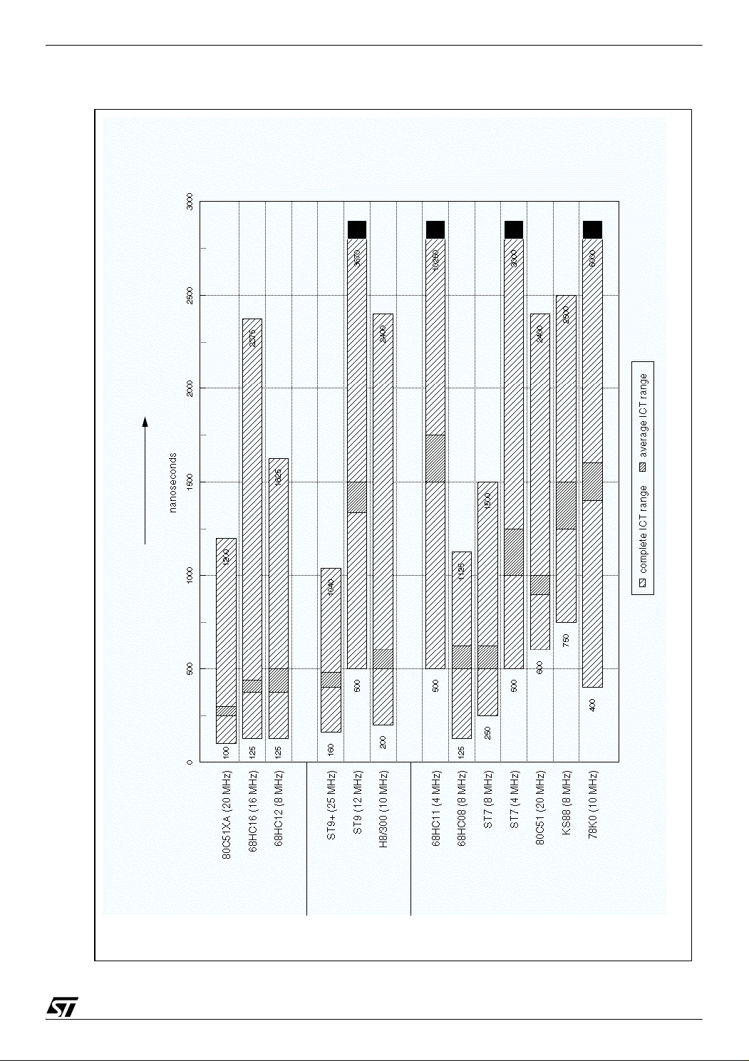
ST7 AND ST9 PERFORMANCE BENCHMARKING
best performance
8-bit MCUs 16-bit MCUs8/16-bit MCUs
Figure 6. Complete and average Instruction Cycle Time ranges
41/51
Page 42

ST7 AND ST9 PERFORMANCE BENCHMARKING
best density
8-bit MCUs 16-bit MCUs8/16-bit MCUs
42/51
Figure 7. Complete and average Instruction Length ranges
Page 43

ST7 AND ST9 PERFORMANCE BENCHMARKING
8 DESCRIPTION OF THE TEST ROUTINES
This section is a more precise description of the test routines. For each test, are detailed the
algorithm, its implementation and the features which it stresses.
8.1 ERATOSTHENES SIEVE
Algorithm
Implementation
Features stressed
The Eratosthenes sieve is a well-known algorithm which searches the prime numbers greater
than or equal 3 out of n elements (n=8189 has been chosen arbitrary).
The even numbers greater than 3 are not prime numbers, so that this algorithm only looks for
prime numbers among an array of odd numbers.
We have chosen an array of 8189 elements. It represents the odd numbers from 3 to 16379. The
array is initialized with the value 'true' ('true' = 0), and is then filled with 1 (false) if the
corresponding number is not a prime number or is not modified (it keeps the value 0='true') if it
is a prime number. Don't forget that it is an array of odd numbers: array[j]
At the beginning of the routine, each number is a potential prime number (initialization value is
'true'). The algorithm consists in setting (to 'false') the odd multiples of every prime number found
in the array skimmed through in the ascending order.
This test measures the elementary computational capability and the ability to manipulate
data in an array.
8.2 ACKERMANN FUNCTION
Algorithm
Implementation
Features stressed It tests the efficiency in recursive procedure calls and in stacks usage.
The Ackermann function is a two parameter function -acker(m,n)- which induces several
recursive calls.
This test routine is performed with two different pairs of parameters: acker(3,5) and acker(3,6).
For instance, with the parameters m=3 and n=6, the function induces 172,
8.3 STRING SEARCH
↔ 2j+3
233 procedure calls.
Algorithm The String search consists in searching a 16-byte string in a 128-character array.
The data are predefined with the following contents:
for the 128-character array,
“xxxxxxxxpatterxxxxxxxxxxxxxxxxxxxxxxxxxxxxxxxxxxxxxxxxxxxxxxxxxxxx” (64 bytes)
“xxxxxxxxxxxxxxxxxpattern is here!xxxxxxxxxxxxxxxxxxxxxxxxxxxxxxx” (64 bytes)
Implementation
Features stressed This program measures the efficiency in data comparison and string manipulation.
and for the 16-byte string,
“pattern is here!” (16 bytes)
The searching algorithm looks for the first matching character in the array and then compares
the rest of the string. If the searched string has been found, it returns the address of the first
character of the string in the array.
43/51
Page 44
ST7 AND ST9 PERFORMANCE BENCHMARKING
8.4 CHARACTER SEARCH
Algorithm The Character search consists in searching a byte in a 40-byte block.
Implementation
Features stressed As the string search, this program measures the efficiency in data comparison.
8.5 BUBBLE SORT
Algorithm The Bubble sort benchmark manages the sorting of a one dimension array of 16-bit integers.
Implementation
Features stressed
8.6 BLOCK MOVE
The data are also predefined. The algorithm searches the byte “o” in the 40-byte block
“-------------------------------o--------”, where the character 'o' is the 32
The test is performed with 10 words and then with 600 words. The array is initialized with 10 or
600 words (16-bit integers) in reverse order.
The algorithm is a classic bubble sort which arranges the 10 words (or the 600 words) in the
ascending order of magnitude.
Note that the routine used is intentionally almost the same for the two values (as though it could
have been optimized for the first value). Few differences may exist, but they do not modify the
way the test is done.
This benchmark demonstrates the efficiency in data comparison and data manipulation but
especially in 16-bit value comparison and 16-bit value manipulation.
nd
character of the block.
Algorithm The Block move test routine aims at transferring a block from a place to another place in memory.
This program is tested with a 64-byte block and with a 512-byte block.
Implementation
Features stressed It shows the data blocks manipulation ability.
Note that the routine used is intentionally almost the same for the two values (as though it could
have been optimized for the first value). Few differences may exist, but they do not modify the
way test is done.
8.7 BLOCK TRANSLATION
Algorithm The Convert test routine aims at transferring a block from a place to another place in memory.
It uses a table to convert the source block into the destination block. The table contains the
Implementation
Features stressed
translation of the source block elements. This benchmark is useful to convert for example from
an ASCII code to an EBCDIC code...
As the block move test program, it shows the data blocks manipulation ability, but also the
ability to use a lookup table.
8.8 16-BIT INTEGER MULTIPLICATION
Algorithm
Implementation
Features stressed This test measures the computational capability of the microcontroller with 16-bit integers.
The 16-bit integer multiplication program performs a multiplication of two unsigned words (16-bit
integers), giving a 32-bit result.
The two operands chosen here are 256, so that the multiplication performed is:
256 x 256 = 65536 (=10000h hexadecimal value)
44/51
Page 45

ST7 AND ST9 PERFORMANCE BENCHMARKING
8.9 16-BIT VALUE RIGHT SHIFT
Algorithm The 16-bit value right shift routine shifts a 16-bit value five places to the right.
Implementation
Features stressed It is a test measuring the word (16-bit) and bit manipulation capability.
8.10 BIT MANIPULATION
The operand to be shifted is 40h (hexadecimal value). It is taken into account as a 16-bit integer
and it is the 16-bit value which is shifted.
Algorithm
Implementation
Features stressed
The Bit manipulation benchmark performs the set, the reset, and the test of 3 bits in a 128-bit
array.
The memory where some bits will be set, reset, and tested, is initialized with the 'Ah' value
(hexadecimal value). It is composed of 8 words '0AAAAh', which represents a 16-byte memory
area, that is to say a 128-bit array.
The test consists in setting, resetting, and then testing the 10th bit of the array, then the 13th bit
of the array, and then the 123
resetting it to 0. And testing a bit is testing it and setting it to 1 if zero (with the zero flag Z also
set if zero).
This benchmark measures the computational capability and the efficiency in bit
manipulation.
rd
bit of the array. Setting a bit is setting it to 1. Resetting a bit is
8.11 TIMER INTERRUPT
Algorithm
Implementation
Features stressed This benchmark measures the interrupt processing performance.
The Timer interrupt benchmark is composed of two routines performing an input capture interrupt
and an input capture/output compare interrupt.
The first routine is the body of an interrupt service routine handling a timer input capture.
The second is the body of an interrupt service routine handling a timer input capture or a output
compare; as interrupt vectors can be separate, this routine may be composed of two different
parts.
The routines include:
• the average instruction (that is an instruction lasting the average instruction cycle time)
which is interrupted and the interrupt entry process (they represent the interrupt latency)
• the body of a typical interrupt service routine including the following operations:
- stack two registers or change register bank (if not done by interrupt processing)
- read timer register
- call to a subroutine with input capture register content as input parameter or output
compare register content as output parameter
- return from subroutine
- unstack registers or restore register bank (if not done by interrupt processing)
- return from interrupt
It is true that each MCU has its specific own manner of handling interrupts. Reading the timer
register and using the input capture/output compare as a parameter for a function call has been
judged as a satisfying way to do so. Thus, it has been chosen as routine body.
45/51
Page 46

ST7 AND ST9 PERFORMANCE BENCHMARKING
9 MEASUREMENT PROCEEDING AND CALCULATION
This section describes measurement proceeding and calculation for computing performance
test routines only. Interrupt processing performance test routines are not concerned
see <Italic>6.2 Core interrupt processing performance<Italic end> for details on measure
(
and calculation).
9.1 MEASUREMENT PROCEEDING
The parameters measured are execution time and code size. The first has been measured
on MCU boards (thanks to an oscilloscope) whenever possible, or with the assembly code.
The second has been measured on the assembly code.
To facilitate execution time measurement, assembly code has been divided in two parts. The
first, called Assignments & Initializations in the source code, contains the initialization of the
MCU and data and then a call to the test routine; which is included in the second part, called
Test Loop. The first part ends with an infinite loop. The execution time and code size will
obviously be measured on Test Loop part.
9.1.1 Execution time measure
An I/O pin is used to make the measure, thanks to a digital oscilloscope. This I/O pin is
configured as an output, with a push-pull, and interrupts are disabled in the initialization part.
The pin used for each MCU is detailed in
Table 13.
Table 13. I/O pins for execution time measuring
MCU name I/O pin for measure
80C51XA pin 0 of port 2
68HC16 pin 2 of port E
68HC12 pin 7 of port E
ST9+ pin 0 of port 4
ST9 pin 0 of port 4
H8/300 pin 0 of port 6
68HC11 pin 0 of port B
68HC08 pin 0 of port A
ST7 pin 0 of port B
80C51 pin 0 of port 1
KS88
78K0 pin 0 port 2
pin 0 of port 2 (for 88C0504)
pin 0 of port 4 (for 88C0116)
The Test Loop routine begins with the set of the I/O pin. This marks the beginning of the test
46/51
Page 47

ST7 AND ST9 PERFORMANCE BENCHMARKING
Theoretical execution time =
number of clock cycles
internal clock frequency
routine and so the start of the measure on the oscilloscope (trigger on positive edge). The
following lines are the implementation of the algorithm. This part ends with the reset of the I/O
pin and a return of the call.
The execution time is the length of the pulse triggered with the oscilloscope. Figure 8. shows
the diagram of the way of execution time measurement proceeding.
Note that it was sometimes not possible to implement all the tests on an MCU (see
<Italic>9.2.2 Memory considerations<Italic end>). In some of these cases, test routines have
even been written and execution time has been calculated theoretically. The theoretical
execution time is simply given by dividing the number of clock cycles, calculated the assembly
source, by the internal processing frequency:
Note that experience has shown the accuracy of these theoretical calculations in front of real
measures. Thus results of both types can be compared.
Figure 8. Execution time measurement proceeding
Assignments &
Initializations
.....
reset I/O pin
.....
.....
Test routine
Execution time
Infinite Loop
Infinite Loop
Test Loop
set I/O pin
.....
.....
.....
.....
reset I/O pin
pulse
Oscilloscope screen
47/51
Page 48

ST7 AND ST9 PERFORMANCE BENCHMARKING
9.1.2 Code size measure
Code size is measured with the assembly code. The result is the number of bytes used to
code the test routine (in Test Loop part) without the set and reset instructions for the I/O pin.
Here is an example of a Test Loop:
0000 C290 test: setb p1.0 ; set I/O pin
0002 7809 mov r0, #srcpointer ; beginning of test routine
0004 7982 mov r1, #destpointer
0006 900200 mov dptr, #200h
0009 7F79 mov r7, #121
000B E6 loop: mov a, @r0
000C 93 movc a, @a+dptr
000D F7 mov @r1, a
000E 08 inc r0
000F 0A inc r2
0010 DFF9 djnz r7, loop ; end of test routine
0012 D290 finish: clr p1.0 ; reset I/O pin
0014 22 ret
The code size of this assembly code equals (12h-2h) = 10h = 16d, thus 16 bytes.
9.2 CALCULATION
9.2.1 Execution time and code size ratios
From execution time and code size measures, preliminary ratios with ST9+ MCU as
reference have been calculated for each test. Using those results, a global execution time
ratio and a global code size ratio have been calculated as an average of all ratios.
As all the tests could not have been implemented on all MCUs (see <Italic>9.2.2 Memory
considerations<Italic end>), one or two different results are presented for each MCU. The
first one, available for all the MCUs, has been calculated with the reduced set of tests
performed on all the MCUs (
Table 14). The second one, only available for some MCUs, has
been calculated with the full set of tests (Table 15).
Table 14. Reduced set of tests
Tests concerned string, char, bubble(10 words), blkmov(64 bytes), convert, 16mul, shright, bitrst
sum(ET ratios of reduced set)
number of tests of reduced set
sum(CS ratios of reduced set)
number of tests of reduced set
Resulting ratio formulas
ET = execution time
CS = code size
Global ET ratio for reduced set =
Global CS ratio for reduced set =
48/51
Page 49

Table 15. Full set of tests
ST7 AND ST9 PERFORMANCE BENCHMARKING
Tests concerned
Resulting ratio formulas
ET = execution time
CS = code size
string, char, bubble(10 words), blkmov(64 bytes), convert, 16mul, shright, bitrst
sieve, acker(3,5), acker(3,6), bubble(600 words), blkmov(512 bytes)
Global ET ratio for full set =
Global CS ratio for full set =
sum(ET ratios of full set)
number of tests of full set
sum(CS ratios of full set)
number of tests of full set
9.2.2 Memory considerations
The “place” of the memory (internal or external) of the MCU used for stack, has indirectly
a consequence on the results. As all the MCUs own internal memory and do not own external
memory, internal memory has been used for most of the tests. But because some tests
(especially Ackermann function) require an important stack capacity, alternative solutions
have been elaborated.
Here is a synthesis of the different cases:
• for tests with a limited memory need, internal memory has been used as stack
• for tests with important memory need,
- for MCUs with important internal memory available, internal memory has been used
- for MCUs with limited internal memory but with external memory (with identical access time)
available, external memory has been used
- for MCUs with limited internal memory and external memory with longer access time, no real
measure has been made in order not to disfavour some MCUs; in some of these cases,
theoretical measures have been calculated based on the assembly code - note that
theoretical results are closed to practical results with internal memory
A small number of tests for some MCUs could not have been implemented due to various
reasons.
49/51
Page 50

ST7 AND ST9 PERFORMANCE BENCHMARKING
As theoretical results are close to actual results with internal memory (see <Italic>9.1.1
Execution time measure<Italic end>), there are only two main cases (for each MCU):
• tests which have been performed (theoretically or practically with internal or external memory)
• tests which have not been implemented (due to various reasons)
As a matter of facts, there are two different sets of tests:
•the reduced set of tests performed on all the MCUs
•the full set of tests performed only on some MCUs
A rapid view on results show that the ratios obtained using both set of tests are not very
different (
see <Italic>4.1 Preliminary remark<Italic end>).
50/51
Page 51

ST7 AND ST9 PERFORMANCE BENCHMARKING
“THE PRESENT NOTE WHICH IS FOR GUIDANCE ONLY AIMS AT PROVIDING CUSTOMERS WITH INFORMATION
REGARDING THEIR PRODUCTS IN ORDER FOR THEM TO SAVE TIME. AS A RESULT, STMICROELECTRONICS
SHALL NOT BE HELD LIABLE FOR ANY DIRECT, INDIRECT OR CONSEQUENTIAL DAMAGES WITH RESPECT TO
ANY CLAIMS ARISING FROM THE CONTENT OF SUCH A NOTE AND/OR THE USE MADE BY CUSTOMERS OF
THE INFORMATION CONTAINED HEREIN IN CONNECTION WITH THEIR PRODUCTS.”
Information furnished is believed to be accurate and reliable. However, STMicroelectronics assumes no responsibility for the consequences
of use of such information nor for any infringement of patents or other rights of third parties which may result from its use. No license is granted
by implication or otherwise under any patent or patent rights of STMicroelectronics. Specifications mentioned in this publication are subject
to change without notice. This publication supersedes and replaces all information previously supplied. STMicroelectronics products are not
authorized for use as critical components in life support devices or systems without express written approval of STMicroelectronics.
The ST logo is a registered trademark of STMicroelectronics.
All other names are the property of their respective owners
© 2004 STMicroelectronics - All rights reserved
STMicroelectronics group of companies
Australia – Belgium - Brazil - Canada - China – Czech Republic - Finland - France - Germany - Hong Kong - India - Israel - Italy - Japan -
Malaysia - Malta - Morocco - Singapore - Spain - Sweden - Switzerland - United Kingdom - United States of America
www.st.com
51/51
 Loading...