

Page 1

AN900
APPLICATION NOTE
INTRODUCTION TO SEMICONDUCTOR TECHNOLOGY
by Microcontroller Division Applications
INTRODUCTION
An integrated circuit is a small but sophisticated device implementing several electronic functions. It is made up of two major parts: a tiny and very fragile silicon chip (die) and a package
which is intended to protect the internal silicon chip and to provide users with a practical way
of handling the component. This note describes the various “front-end” and “back-end” manufacturing processes and tak es the transistor as an example, beca use it uses the MOS technology. Actually, this technology is used for the m a jority of the ICs manufactu red at STMicroelectronics.
AN900/1100 1/15
1
Page 2
INTRODUCTION TO SEMICONDUCTOR TECHNOLOGY
1 THE FABRICATION OF A SEM ICONDUCTOR DEVICE
The manufacturing phase of an integrated c ircui t can be d ivided into two steps. The firs t,
wafer fabrication , is the extreme ly sop histicated and intricate proces s of manufa cturing the
silicon chip. The second, assembly, is the highly precise and automated process of pack-
aging the die. Those two phases are commonly known as “Front-End” and “Back-End”. They
include two test steps: wafer probing and final t est.
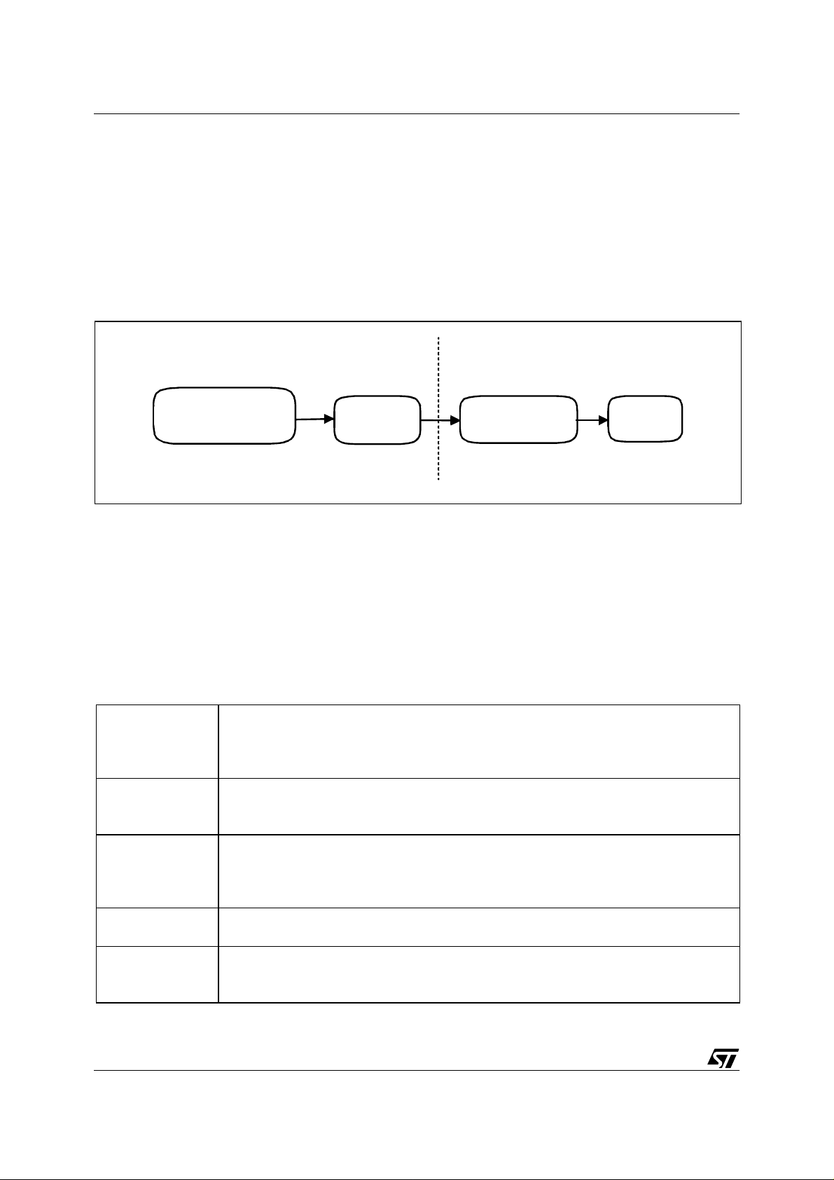
Figure 1. Manufacturing Flow Chart of an Integrated Circuit
"Front-End" "Back-End"
WAFER
FABRICATION
Wafer
Probing
ASSEMBLY
Final
Test
VR02103A
1.1 WAFER FABRICATION (FRONT-END)
Identical integrated circuits, called die, are made on each wafer in a multi-step process. Each
step adds a new la ye r t o th e w afer or mod ifies the e xis ting o ne . Thes e l ayer s fo rm t he e lements of the individual electronic circuits.
The main steps for the fabrication of a die are summarized in the following table. Some of
them are repeated several times at different stages of the process. The order given here
doesn't reflect the real order of fabrication process.
This step shapes the different components. The principle is quite simple (see draw-
PhotoMasking
Etching
Diffusion
Ionic
Implantation
Metal
Deposition
ing on next page). Resin is put down on the wafer which is then exposed to light
through a specific mask. The lighten part of the resin softens and is rinsed off with
solvents (developing step).
This operation removes a thin film material. There are two different methods: wet
(using a liquid or soluble compound) or dry (using a gaseous compound like oxygen
or chlorine).
This step is used to introduce dopants inside the material or to grow a thin oxide
layer onto the wafer. Wafers are inserted into a high temperature furnace (up to
1200 ° C) and doping gazes penetrate the silicon or react with it to grow a silicon
oxide layer.
It allows to introduce a dopant at a given depth into the material using a high energy
electron beam.
It allows the realization of electrical connections between the different cells of the
integrated circuit and the outside. Two different methods are used to deposit the
metal: evaporation or sputtering.
2/15
2
Page 3

INTRODUCT ION TO SEMICO NDUCTOR TE CHNOLOGY
Wafers are sealed with a passivation layer to prevent the device from contamina-
Passivation
Back-lap
tion or moisture attack. This layer is usually made of silicon nitride or a silicon oxide
composite.
It’s the last step of wafer fabrication. Wafer t hickness is reduced (for microcontroller
chips, thickness is reduced from 650 to 380 microns), and sometimes a thin gold
layer is deposited on the back of the wafer.
Initially, the silicon chip forms part of a very thin (usually 650 microns), round silicon slice: the
raw wafer. Wafer diameters are typically 125, 150 or 200 mm (5, 6 or 8 inches). However raw
pure silicon has a main electrical property: it is an isolating material. So some of the features
of silicon have to b e altered, b y means of well controlled proc esses. This is obtained by
"doping" the silicon.
Dopants ( or do ping a tom s) ar e purp osely ins e rted in th e silic on lat tice, he nce c han ging t he
features of the material in predefined areas: they are divided into “N” and “P” categories representing t he negative and positive carriers they hold. M any di ffere nt do pants a re u se d to
achieve these desired features: Phosphorous, Arsenic (N type) and Boron (P type) are the
most frequently used ones. Semiconductors manufacturers purchase wafers predoped with N
or P impurities to an i mpurity level of.1 ppm (one doping atom per ten million atoms of silic on).
There are two ways to dope the silicon. The first one is to insert the wafer into a furnace.
Doping gases are then introduced which impregnate the silicon surface. This is one part of the
manufacturing process called diff usi on (the other part being the oxide grow th). The second
way to dope the silicon is called ionic impl antation. In this case, doping atoms are introduced
inside the silicon using an ele ctron beam. Un like diffusion, ionic implant ation allows to put
atoms at a g iven de pth ins ide the silicon and bas ically allows a better contr ol of all t he ma in
parameters dur ing the pr ocess . Io ni c im plant ation proc ess is si mpler than d iffus ion proc ess
but more costly (ionic implanters are very expensive machines).
3/15
Page 4
INTRODUCTION TO SEMICONDUCTOR TECHNOLOGY
Figure 2. Diffusion and Ionic Implanta tion Processes
DIFFUSI ON PROCESS
OXIDE GROWTH
Oxygen (O )
2
SiO
DIFFUSION FURNACE
DOPING DOPING
HIGH TEMPERATURE
Doping atoms
2
IONIC IMPLANTATION
PROCESS
Electron Beam
VACUUM
IONIC IMPLANTER
VR02103B
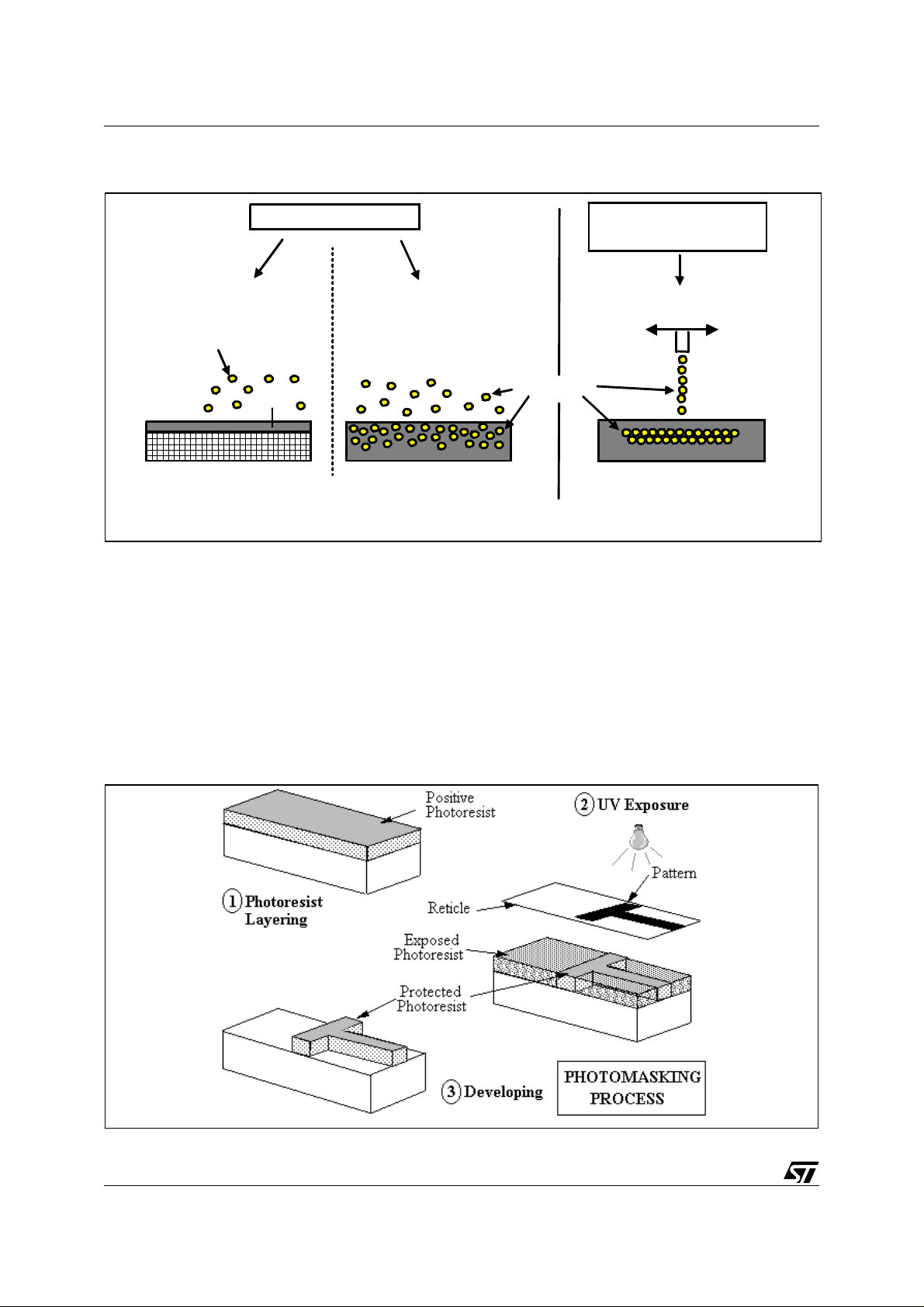
Photomasking (or masking) is an operation that is repeated many times dur ing the process.
This operation is described on the above graph. This step is called photomasking because the
wafer is “masked” in some areas (using a specific pattern), in the same way one “masks out”
or protects the windscreens of a car before painting the body. But even if the process is somewhat similar to the painting of a car body, in the case of a silicon chip the dimensions are
measured in tenth of m icro ns. The photoresi st will replicate this pattern on the wafer. The exposed p art of th e photor esist is then rinsed o ff wit h a solve nt (usu ally hy drofl uoric or phos phoric acid).
Figure 3. Photomasking Process
4/15
Page 5
INTRODUCT ION TO SEMICO NDUCTOR TE CHNOLOGY
Metal dep osi ti o n is used to put down a metal layer on the wafer surface. There are two ways
to do that. The process shown on the graph below is called sputtering. It consists first in creating a plasma with argon ions . These ions bump into the target surface (composed of a metal,
usually aluminium) and rip metal atoms from the target. Then, atoms are projected in all the directions and most of them condense on the substrate surface.
Figure 4. Metal Deposition Process
POWER SUPPLY
CATHODE
METAL
ATOMS
PLASMA
Thin Metal Layer
SUBSTRATE
ANODE
VR02103C
Etching process is used to etch into a specific layer the circuit pattern that has been defined
during the photomasking process. Etching process usually occurs after deposition of the layer
that has to be etched. Fo r instance, the poly gates of a transistor are obtained by etching the
poly layer. A second example are the aluminium connections obtained after etching of the aluminium layer.
Figure 5. Etching Process
Photoresist Mask
Thin Film to be etched
BEFORE
Substrate
AFTER
VR02103D
5/15
Page 6

INTRODUCTION TO SEMICONDUCTOR TECHNOLOGY
Photomasking, ionic implantation, diffusion, metal deposition, and etching processes
are repeated many tim es, us ing differen t m ateri als and do pant s at di fferen t tempe ratures in
order to achieve all the operations needed to produce the requested characteristics of the silicon chip. The resolution limi t (mini mal line s ize inside the circuit) of current technology is 0.35
microns. Achieving such results requires very sophisticated processes as well as superior
quality levels.
Backlap is t he fi na l step of wa fe r fa br ic ati on . The w af er th i ckn ess is re du c ed fr om 6 50 m icrons to a minimum of 180 microns (for smartcard products).
Wafer fabrication takes place in an extremely clean environment, where air c leanliness is one
million times b e tter than the air we normally breathe in a city, or some orders of magnitude
better than the air i n a heart t ransplant operating th eatr e. Photom a sking, for e xampl e, tak es
place in rooms where there’s maximum one particle whose diameter is superior to 0.5 micron
(and doesn’t exceed 1 micron) inside one cubic foot of air.
All these processes are part of the m anufacturing phase of the chip itself. Si licon chips are
grouped on a silicon wafer (in the same w ay postage stamps are printed on a single sh eet of
paper) before being separated from each other at the beginning of the assembly phase.
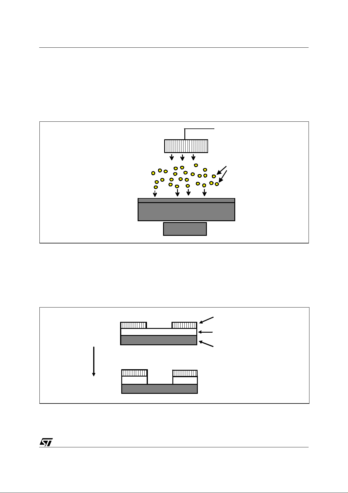
Wafer Probing. This step takes place between wafer fabrication and assembly. It verifies the
functionality of the device performing thousands of electrical tes ts, by means of special microprobes (see graph on next page). Wafer probing is composed of two different tests:
1. Process parametric test: this test is performed on some test samples a nd checks the
wafer fabrication process itself.
2. Full wafer probing test: this test verifies the functionality of the finished product and is performed on all the dies.
Figure 6. Description of the Wafer Probing Operation
The bad di e are au toma tical ly mark ed wi th a bl ack dot so they can be separated from the
good die after the wafer is cut. A record of what went wrong with the non-working die is closely
examined by fa ilure an alysis en gin eers to de term ine w here th e problem occ urred s o that it
may be corrected. The percentage of good die on an individual wafer is called its yield.
6/15
Page 7

INTRODUCT ION TO SEMICO NDUCTOR TE CHNOLOGY
1.2 ASSEMBLY (BACK-END)
The first step of assembly is to separate the silicon chips: this step is called die cutting.
Then, the die are placed on a lead frame: the “leads” are the chip legs (which will be soldered
or placed in a socket on a printed circuit board. On a surface smaller than a baby's fingernail
we now have thousands (or millions) of electronic components, all of them interconnected and
capable of implementing a subset of a complex electronic function. At this stage the device
is completely func tional , but i t wo uld be imp ossible to u se it w ithout som e sor t of s upporting
system. Any scratch would alter its behaviour ( or impact its r eliabili ty), any shock would cause
failure.
Therefore, the die must be put into a ceramic or plastic package to be protec ted fr om the external world. A number of operations have to be made to realize this: they are described on the
following graph.
7/15
Page 8

INTRODUCTION TO SEMICONDUCTOR TECHNOLOGY
Figure 7. Description of The Assembly Process
Wires thinner than a human hair (for microcontrollers the typical v alue is 33 microns) are re-
quired to connect chips to the external world and enable electronic signals to be fed through
the chip. The process of connecting these thin wires from the chip’s bond pads to the package
lead is called wire bonding (see also graph on next page for more details).
Figure 8. Wire Bonding
8/15
Page 9

INTRODUCT ION TO SEMICO NDUCTOR TE CHNOLOGY
Figure 9. Wire Bonding Operation
The chip is then mounted in a ceramic or plastic package. The package not only protects the
chip from e xternal shock s, bu t als o ma kes the whol e de vice eas ier to hand le. T heses pack ages come in a variety of shapes and sizes depending on the die itself and the application in
which it will be used.
9/15
Page 10

INTRODUCTION TO SEMICONDUCTOR TECHNOLOGY
Figure 10. Different Kinds of Plastic Packages
Products are then marked with a “tr aceability co de” which is used by the m anufacturer and
the user to identify the function of the device (and its date of fabrication). At the end of the assembly proc ess, th e int egrat ed cir cuit is tes te d b y aut omat ed test equ ipment. O nly the inte grated circuits that passed the tests will be packed and shipped to their final destination.
10/15
Page 11

INTRODUCT ION TO SEMICO NDUCTOR TE CHNOLOGY
2 BASIC IC ELEMENT: THE TRANSISTOR
2.1 MOS TECHNOLOGY
We will examine first the basics of MOS (Metal Oxide Semiconductor) technologies as they
are used for the majority of the integrated circuits manufactured at STMicroelectronics.
. There are three major MOS technology families: PMOS, NMOS and CMOS. They refer to the
channel type of the MOS transistors made with the technology.
– PMOS technologies implement P-channel transistors by diffusing P-type dopants (usually
Boron) into an N-type silicon substrate to form the source and the drain. P-channel is so
named because the channel is composed of positively charged carriers.
– NMOS technologies are similar, but use N-type dopants (usually Phosphorus or Arsenic)
to make N-channels transistors in P-type silicon substrate. N-channel is so named because
the channel is composed of negatively charged carriers.
– CMOS (Complementary MOS) technologies combine both P-channel and N-channel de-
vices on the same silicon. Either P or N-type silicon substrates can be used. However, deep
areas of the opposite doping type (called wells) must be defined to allow fabrication of the
complementary transistor type.
Figure 11. MOS Technologies
11/15
Page 12

INTRODUCTION TO SEMICONDUCTOR TECHNOLOGY
Most of the early semiconductor devices were made with PMOS technologies because it was
easier to obtain stable manufacturing process with this technology. As higher speeds and
greater densities were needed, new devices were implemented with NMOS. This was due to
the higher speed of N-channel charge carriers (electrons) in silicon and also to the progress in
the control of silicon doping. But CMOS technology has begun to see widespread commercial
use in memory devices: it allowed the use of very low power devices. At the beginning, CMOS
were slower than NMO S devices. T oday, CMO S technology has been improved to pr oduce
higher speed devices.
2.2 FABRICATION OF A TRANSISTOR
The fabrication begins with a slice of single crystal silicon, uniformly doped P-type.
The wafer is oxidized in a furnace to grow a thin
layer of silicon dioxide (SiO
) on the surface. Sil-
2
icon nitride is then deposited on the oxidized
wafer in a gas phase chemical reactor. The wafer
is now ready to receive the first patt e rn of what is
to become a many layered complex circuit. The
first pattern defines the boundaries of the active
regions of the integrated circuit, whe re transistors, capacitors, diffused resistors and first level
interconnects will be made.
The patterned wafer is th en im plante d wi th bor on
atoms. Boron will only reach the etched zones of
the silicon substrate, creating P-type doped
areas that will electrically separate active are as.
Wafer is oxidized again and the thick oxide only
grows in the etched areas due to silicon nitride’s
properties as an oxidation barrier.
The remaining silicon nitride layer is re moved.
Now that the areas for active transistors have
been defined and isolated, the transistor types can be determined. The wafer is patterned and
implanted with dopant atoms.The energy and dose at which the dopant atoms are implanted
determines much of the transistor’s characteristics.
The transistor types defined, the gate oxide of the
active transistors are grown in a high temperature
furnace. The gate oxide layer is then mas ked and
holes are etched to provide direct access to buried
contacts where needed . A po lycristalin e sili con
layer is deposited on th e w afer. The gate layer is
then patterned to define the actual transistor gates
and interconnect paths.
12/15
Page 13

INTRODUCT ION TO SEMICO NDUCTOR TE CHNOLOGY
Wafer is diffused with N-type dopant s to form the
source and drain junction. The transistor gate
material ac ts a s a b ar rier t o th e dop ant p r ovidi ng
an undiffused channel self-aligned to the two j unc-
tions. The wafer is then oxidized to seal the junc-
tions from contamination with a layer of SiO
.
2
A thick glass layer is then deposited over the wafer
(to provide better insulation), patterned with con-
tact holes and placed in a high temperature fur-
nace. Metal is deposited on the wafer and the in-
terconnect patterns and external bonding pads are
defined and etched. To prevent the device from
contami nation or moistu re attac k, wafers are
sealed with a passivation layer. Patterning is
done for the last time opening up windows only
over the bond pads where external connections
will be made.
This completes basic fabrication sequence for a
single poly and single metal layer process.
13/15
Page 14

INTRODUCTION TO SEMICONDUCTOR TECHNOLOGY
2.3 HOW DOES A TRANSISTOR WORK?
Transist or is the basic elem ent of an MCU device. There c an be hu ndred s of thou san ds of
them and the size of their gate can go down to 0.35 microns.
Let’s explain the way a N MOS trans istor o perates . Basic ally, T here’s a lack of ele ctrons be tween the Source (S) and the Drain (D ) because this area has been implanted with a P-type
dopant (Boron for instance). Therefore, when no voltage is applied, there’s no current between
the source and the drain (case of the enhancement tran sistor).
If we apply a positive voltage on the gate and the drain, then this will attract electrons in the
channel existing between the source and the drain, therefore making it possible for an elec-
trical current to flow between S and D.
There are two main types of transistor:
– Enhancement Transistor: channel is permanently OFF. It requires a positive applied gate
voltage to turn on. Microcontrollers, for instance, mainly use this type of transistor.
– Depletion Transistor: channel is permanently ON. It requires a negative applied gate volt-
age to turn off.
This schem e is a c ross s ection of
a real transistor obtained after
about 100 steps of fabrication
(see previous paragraph for the
explanation of the different fabrication steps). The last layer is
called a passivation layer and protects the transistor.
14/15
Page 15

INTRODUCT ION TO SEMICO NDUCTOR TE CHNOLOGY
“THE PRESENT NOTE WHICH IS FOR GUIDANCE ONLY AIMS AT PROVIDING CUSTOMERS WITH INFORMATION
REGARDING THE IR PRO DUCT S IN OR DER FO R THEM TO SAV E TIME . AS A RES ULT, STMIC ROEL ECTR ONI CS
SHALL NOT BE HELD LIABLE FOR ANY DIRECT, INDIRECT OR CONSEQUENTIAL DAMAGES WITH RESPECT TO
ANY CLAIMS ARISING FROM THE CONTENT OF SUCH A NOTE AND/OR THE USE MADE BY CUSTOMERS OF
THE INFORMATION CONTAINED HEREIN IN CONNEXION WITH THEIR PRODUCTS.”
Information furnished is believed to be accurate and reliable. However, STMicroelectronics assumes no responsibility for the consequences
of use of such information nor for any infringement of patents or other rights of third parties which may result from its use. No license is granted
by implic ation or otherwise under any patent or patent ri ghts of STM i croelectr oni cs. Specifications mentioned in thi s publicati on are subject
to change without notice. This publication supersedes and replaces all information previously supplied. STMicroelectronics products are not
authorized for use as cri tical comp onents in life support dev i ces or systems wi thout the express written approv al of STMicroel e ctronics.
The ST logo is a registered trademark of STMicroelectronics
2000 STMicroelectronics - All Rights Reserved.
Purchase of I
Australi a - Brazil - China - Finland - France - Germany - Hong Kong - India - Italy - Japan - Malaysia - Malt a - Morocco - Singapore - Spain
2
C Components by STMicroelectronics conveys a license under the Philips I2C Patent. Rights to use the se components in an
2
C system i s granted pro vid ed that the sy stem conforms to the I2C Standard Specification as defined by Philips.
I
STMicroelectronics Group of Compan i es
Sweden - Switzerland - United K i ngdom - U.S. A.
http://www.s t. com
15/15
 Loading...