

Page 1

AN886
APPLICATION NOTE
SELECTING BETWEEN ROM, FASTROM AND OTP
FOR A MICROCONTROLLER
by Microcontroller Division Applications
INTRODUCTION
A customer who develops an MCU-based application needs various levels of fl exibility in order
to perform code modifications at different times in the life cycle of the product (these levels are
explained on the next page). To satisfy these requirements, STMicroelectronics supports several device types within two main groups of microcontroller product families:
– EPROM, OTP, FASTROM and ROM microcontroller families
– Flash, FASTROM and ROM microcontroller families
This Appli cation Note disc usses t he first g roup of familie s. Fo r infor mation o n the second
group, refer to Application Note AN1068.
Rev. 1.0
AN886/0903 1/9
1
Page 2

SELECTING BETWEEN ROM, FASTROM AND OTP FOR A MICROCONTROLLER
DEFINITION OF TERMS
Windowed EPROM (Erasable Programmable Read Only Mem ory): this type of MC U device
can be program med th en erase d using UV lig ht. EPRO M MCU devices are s old in cera mic
packaging with a quartz window. They are reprogrammable outside systems.
OTP (One Time Programmable EPROM): OTP is a type of EPROM sold in plastic packaging.
Unlike UV EPROMs that have a quartz window in the package above the chip to allow erasure
by UV light, OTP Memory cannot be erased once it has been programm ed. OT Ps ar e typi-
cally programmed by the customer.
FASTROM (Factory Advanced Service Technique Read Only Memory): this type of MCU is a
OTP devic e p re-programmed by ST Microe lectro nics with th e cus tom er’s code and s elec ted
options. The advantage of FASTROM, compared to OTP, is improved programming efficiency
for large quantities (10,000+) and compared to ROM, it has the advantage o f a shorter leadtime.
ROM (Read Only Memory): ROM devices are programmed at the fabrication step usi ng a special mask containing the customer code. Therefore, the code can't be modified after that step.
Costs are highly depending on the flexibility given to the device (ability to be easil y erased or
programmed). ROM is the cheapest technology but provides little flexibility whereas OTP and
EPROM are m ore flex ible but the ir ma nuf actur ing c ost is high er. T he hig h co st of E PRO M
MCU devices is due to the price of ceramic packages.
Figure 1. Cost versus Flexibility for different MCU types
+
COST
_
ROM
_
OTP
FLEXIBILITY
EPROM
+
VR02100A
2/9
2
Page 3
SELECTING BETWEEN ROM, FASTROM AND OTP FOR A MICROCONTROLLER
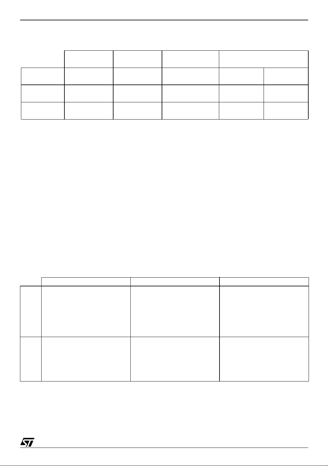
1 TYPICAL APPLICATION DEVELOPMENT FLO W
ST
Solution
Code
Updates
Number
of Units
Design
Phase
EPROM OTP OTP OTP ROM
•••• ••• •• • None
• •• ••• •••• •••••
Validation
Phase
Pre-production
Phase
Production
Phase
When a new application is developed, different device versions will be used at each step of the
development, depending on the required programming flexibilit y .
During the design p hase , a hi gh flexi bility i s r equ ired a nd only a sm all nu mbe r of pa rts are
necessary, therefore the use of UV erasable EPROM is recommended. Then, fewer code corrections (and a significant number of parts) are needed during validation phase: at this point
OTP is the best solution.
The next step is pre-production phase: only a few code updates are needed at a reasonable
device cost. Again, the best choice is to us e OTP memor y. Finally, when the mass produc-
tion phase begins, there is no more need for corrections since the product has been fully optimized, so ROM is the most adapted if very high volumes are needed. Otherwise (low to medium volumes) the mos t effective soluti on is to continue usin g STMicroelec tronics’ comp etitively priced OTP.
The following table summarizes the main benefits and drawbacks of using ROM, OTP or windowed EPROM MCU devices.
ROM OTP EPROM
Cheaper than OTP (simpler
process and testing)
Lower failure rate
+
(less handling, no programming)
Limited flexibility
(customer code implemented
at masking stage)
-
Higher inventory risks
Lower cost compared to windowed EPROM
(use of cheaper plastic packages)
Ability to be programmed di-
rectly by the final user
Higher failure rate compared to
ROM due to customer handling
and programming
High flexibility
(Programming, Code check
and Erasure cycle in less than
60 minutes)
Expensive ceramic packages
3/9
Page 4

SELECTING BETWEEN ROM, FASTROM AND OTP FOR A MICROCONTROLLER
2 COMPARISON OF PRODUCTION FLOWS FOR ROM AND OTP
ROM and OTP devices have exactly the same functional and electrical behaviour in an application because STMicroelectronics designs the two products with the same methodology. ROM
and OTP devices are qualif ied using the same procedures. They ar e tested using the same test
flows (see further) and with the same parameter limits. A good indication of device similarity
is EMC (electromagnetic noise immunity ) measurements performed on both ve rsions (ROM
and OTP) for the same MCU device.
ST6220 (ROM version)
ST62T20 (OTP version)
4/9
Page 5

SELECTING BETWEEN ROM, FASTROM AND OTP FOR A MICROCONTROLLER
3 TYPICA L MANUFACTURI NG LEAD TI ME FOR ROM AND OTP
The complexity of all the operations needed to manufacture a component implies a certain
time period. Understanding STMicroelectronics’ MCU manufacturing cycle is important in
order to establish good relationships with customers. The numbers given here are typical and
subject to change in the future
Figure 2. Typical Fabrication Leadtime in weeks.
Transit Time**
7
5*
1
1
1
1
1
Wafer Fabrication
Stan da rd Wafers*
*Pre-diffused Wafers (Selected Products)
Wafer
Probing
Assembly Final Test Shipment
**Wafer and assembl y s i tes are typical l y located in di f ferent countries.
In order to limit lead time on ROM products, STMicroelectronics has introduced pre-diffusion
technology on selected products. This allows a two weeks reduction in total cycle time. Also
notice that MCU devices have to be ordered in specified minimum quantities for ROM version.
Figure 3. Typical Leadtime for Standard Pro ducts
12
12
Typical
10
Leadtime
for
Standard
Product
(weeks)
4
2*
4
FAST
ROM
Pre-
diffused
ROM
Standard
ROM
Flash
0 - 5,000 units > 5,000 units
* Gold Standard products
> 5,000/10000 units
Min. Quantity
5/9
Page 6
SELECTING BETWEEN ROM, FASTROM AND OTP FOR A MICROCONTROLLER
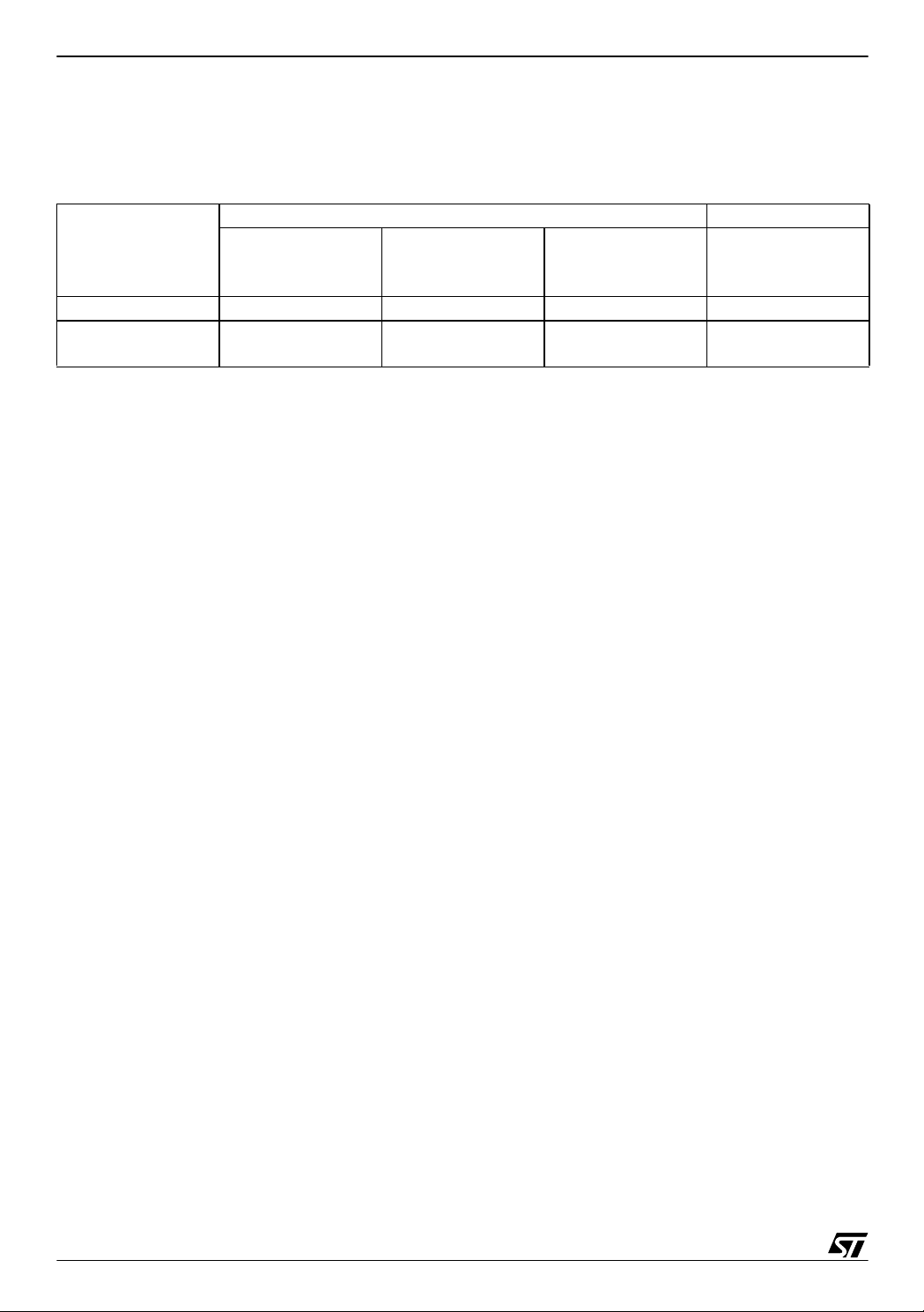
4 MINIMUM ORDER QUANTITIES FOR ROM AN D FASTROM
The following minimum order quantities apply to ROM and FASTROM microcontroller devices:.
ROM FASTROM
Minimum quantity
per year and per
line item
ST6 Family
ST7 and ST9
Families
Minimum quantity
per year
100000 50000 10000 5000
50000 25000 5000 5000
Minimum order
quantity
Minimum quantity
per line item
6/9
Page 7

SELECTING BETWEEN ROM, FASTROM AND OTP FOR A MICROCONTROLLER
5 OTP RELIABILITY
Why do ROM devices have very low failure rates?
For ROM parts, the customer program is included at a specific mask level of the wafer fab-
rication. There fore, the c omplete pr oduct fun ctiona lity is present in both th e die and the as sembled p roduc t. Thi s functi onali ty can be fully ev aluate d at bo th wafer probing and final
electrical test, thus ensuring a low reject rate at customer manufacturing stage.
Testing Programmability and Data Retention for OTP device s
To ensure optimal OTP quality, STMicroelectronics tests two important device characteristics:
programmability and data retention. The program memory of an OTP should be seen as a
number of cells that will be activated during programming. These cells can be “deactivated” by
lighting the die with UV light. This recovery is no longer possible once the OTP die has been
encapsulated in an opaque plastic package. Therefore programmability and data reten tion
can only be fully tested at wafer probing.
At this step the dice are electrically tested and the memory is programmed to verify program-
mability. Then the w afers a re pla ced in high te mper ature bake to accelerate any possible
memory retention defects. The dice are then tested again to check data r e te n tio n . After this
test, UV light is used to deactivate the cells and the good dice are assembled.
Description of OTP programmability test
Figure 4. Details about the electrical tests performed on OTP and ROM
ROM
OTP
Tested
Feature
Full Electr ical
TEST
Memory Check
Full Electrica l
TEST
OTP Programming
Memory Check
Programmability
WAFER PROBING
BAKE
Full Electrical
TEST
Memory Check
Inking
Data Retention
FINAL TEST
Full Electrical
TEST
Memory Check
Full Electric al
TEST
Memory Check
(reserved number
of bytes)
VR02100E
Although the programmability of the OTP die is verified as fully functional at probe test, the assembly proce ss can affect this parameter in the finished product (for example by damaging
some cells). It is therefore necessary to make a final test to check programmability. But
since UV light cannot be used to restore OTP's programmed bytes once the die has been en-
7/9
Page 8

SELECTING BETWEEN ROM, FASTROM AND OTP FOR A MICROCONTROLLER
capsulated, it is not possible to test 100% of the user program area. For this reason the final
test is limited to a reserved number of bytes which are programmed and then verified.
OTP rejects rates due to programmability failures
As the programmability of the OTP cannot be fully tested once the die has been encapsulated,
a customer is likely to find a programming reject rat e below 1% when pr ogrammi ng is performed using qualif ie d pr o gramming tools . This rate should be considered as normal for
OTPs and shoul d not ge nera te customer quality returns. If higher failure rates are observed,
it is recommended to check the programming equipment.
Recommended screening conditions for OTP (data retention failures)
Programmability f a ilures can be fully screened because gang programmers check the con-
tent of OTP devices after programmi ng. But gang programm ers cannot perform data retention tests.
High temperature aging is recommended for screening microcontrollers that use OTP devices
and performing data retention tests. The well-known retention failure mechanism corresponds
to charge losses during the component life time. The customer i s likely to find a data reten tio n
failure rate below 0.5% when programming is performed using qualified programming
tools. Therefore, it is strongly recommended to screen these poten tial failures as described
hereafter:
Figure 5. Recommended Screening Conditions for OTP
PROGRAM
PROGRAM
VERIFY
Programmability
Failures
HIGH
TEMPERATURE
AGING
Nitrogen atmosphere
150 ø C / 24 h
Normal atmosphere
125 ø C / 48 h
PROGRAM
VERIFY
Data Retention
Failures
MOUNT
VR02100F
Screening devices that are subject to data retention failures will allow customers to obtain
OTP devices with a similar quality level compared to ROM devices.
In order to further lower the reject levels for programmability and data retention, STMicroelectronics is continuously pursuing technology improvements in areas as soft die m ounting, low
stress mold compounds and passivation layer enhancements.
8/9
Page 9

SELECTING BETWEEN ROM, FASTROM AND OTP FOR A MICROCONTROLLER
“THE PRESENT NOTE WHICH IS FOR GUIDANCE ONLY AIMS AT PROVIDING CUSTOMERS WITH INFORMATION
REGARDING THE IR PRO DUCT S IN OR DER FO R THEM TO SAV E TIME . AS A RES ULT, STMIC ROEL ECTR ONI CS
SHALL NOT BE HELD LIABLE FOR ANY DIRECT, INDIRECT OR CONSEQUENTIAL DAMAGES WITH RESPECT TO
ANY CL AIM S AR IS IN G FR OM T HE CO N TENT OF S UC H A NO TE A ND /O R T HE U SE M AD E BY C US TO ME RS O F
THE INFORMATION CONTAINED HEREIN IN CONNECTION WITH THEIR PRODUCTS.”
Information furnished is believed to be accurate and reliable. However, STMicroelectronics assumes no responsibility for the consequences
of use of such information nor for any infringement of patents or other rights of third parties which may result from its use. No license is granted
by implic ation or otherwise under any patent or patent ri ghts of STM i croelectr oni cs. Spec i fications mentioned i n this publication are subje ct
to change without notice. This publication supersedes and replaces all information previously supplied. STMicroelectronics products are not
authorized for use as cri tical comp onents in life support dev i ces or systems wi thout exp res s written ap proval of STMi croelectr onics.
The ST logo is a registered trademark of STMicroelectr oni cs.
All other n am es are the pro perty of thei r respectiv e owners
© 2003 STMi croelectronics - All rights reserved
STMicroelectronics GROUP OF COMPANIES
Australi a – B elgium - Brazil - Canada - China – Czech Republ i c - Finland - F rance - Germany - Hong Kong - India - Is rael - Italy - Japan -
Malaysia - Malta - Morocco - Singapore - Spain - Sweden - Switzerland - United Kingdom - United States
www.st.com
9/9
 Loading...