

AN880
®
THE L6569: A NEW HIGH VOLTAGE IC DRIVER FOR
INTRODUCTION
Electronic lamp ballasts are now popular in both
consumer and industrial lighting. They offer power
saving, flicker free operation and reduced sizes.
Improvements to the light control and cost reduction of the ballast will broaden the ir market acceptance.
Today designers focus on reducing the cost of the
ballast, but also work to add features to the ballast like saving energy by dimming the light, or increasing the life time with better preheat and protections. Such requirements have contributed to
the development of dedicated high voltage controllers like the L6569, which ar e able to driv e the
floating transistor of a symmetric half bridge inverter. This device is a simple, monolithic oscillator-half bridge driver that allows quick design of
the ballast.
HIGH VOLTAGE I C DRI VERS I N B ALL AST APPLICATIONS
The voltage fed half bridge
Voltage fed series resonant half bridge inverters
are currently used for Compact Fl uorescent Lamp
ballasts (CFL), for Halogen Lamp transformers,
and for many European Tube Lamp (TL) ballasts.
This simple converter is preferred for new designs, because it minimizes the off state voltage
of the power transistors to the peak line voltage,
and requires only one resonant choke. In addition
this choke protects the half bridge against short
circuits across lamp terminals. However overheating and overcurrent occur during open load operation. The inverter robustness must be improved, or some protections are required.
The half bridge inverter operates in Zero Voltage
Switching (ZVS) resonant mode [1], to reduce the
transistor switching losses and the electromagnetic interference generated by the output wiring
and the lamp.
Fully integrated ballast controllers
By varying the switching frequency, the half
bridge inverter is able to modulate the lamp
power. However most current designs use a sin-
APPLICATION NOTE
ELECTRONIC LAMP BALLAST
by G. Calabrese and T. Castagnet
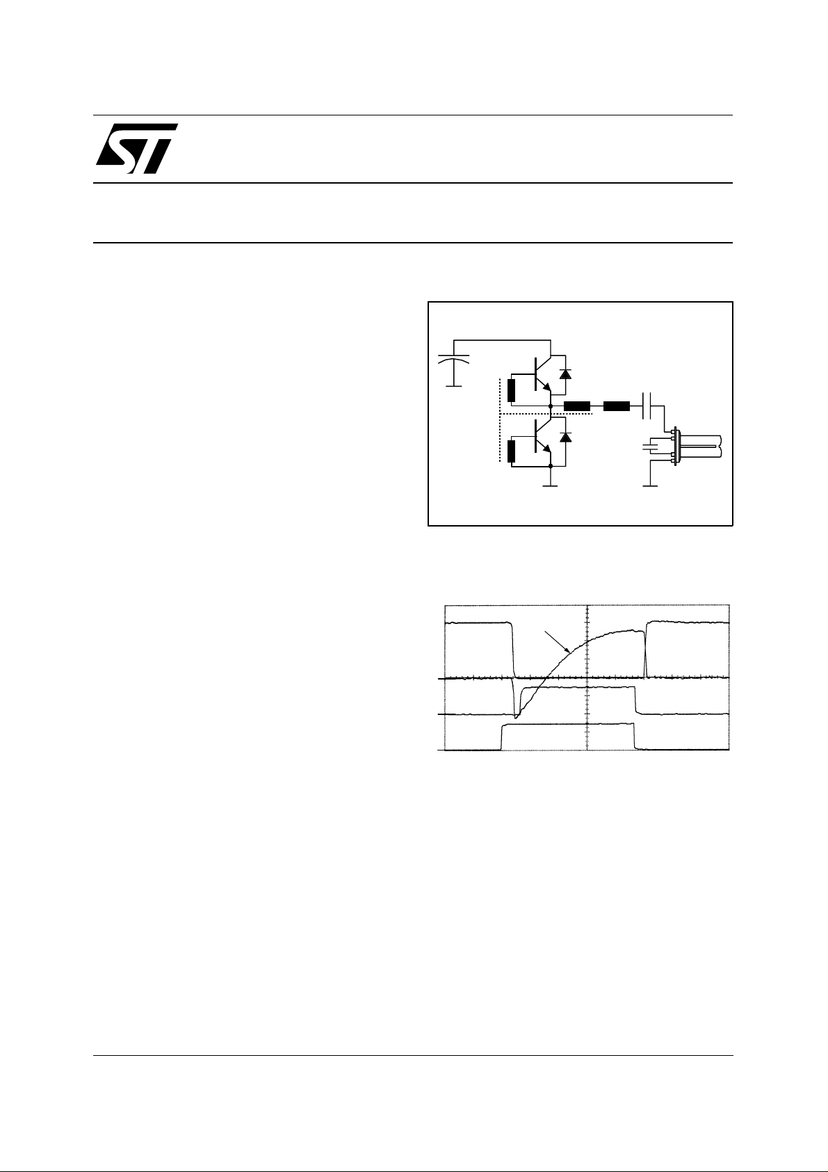
Figure 1: CFL series resonant half bridge inverter.
Figure 2: Current and voltage of the STD3NA50
MOSFETs when driven in ZVS with
the L6569.
I
V
DS
GND
GND
GND
gle frequency with a saturable pulse transformer
(see fig. 1) to drive the transistors. This type of
design has a higher component count, a higher
tolerance on the switching frequency, and it cannot adjust the lamp power.
The only way to design a cost effective, compact
and smart control of the lamp is to use a dedicated I.C. that is able to drive the upper transistor
of an symmetric half bridge inverter. Such controllers require a high voltage capability for the floating transistor driver [2]. MOSFETs are preferred
over Bipolar transistors as power switches because their gate driver requires a lower supply
current and a smaller silicon size [3].
D
LVG
RF
2 µs/dv ; 50 V/dv ; 0.1 A/dv
February 2003
1/14
AN880 APPLICATION NOTE
THE L6569 AND ITS APPLICATIONS
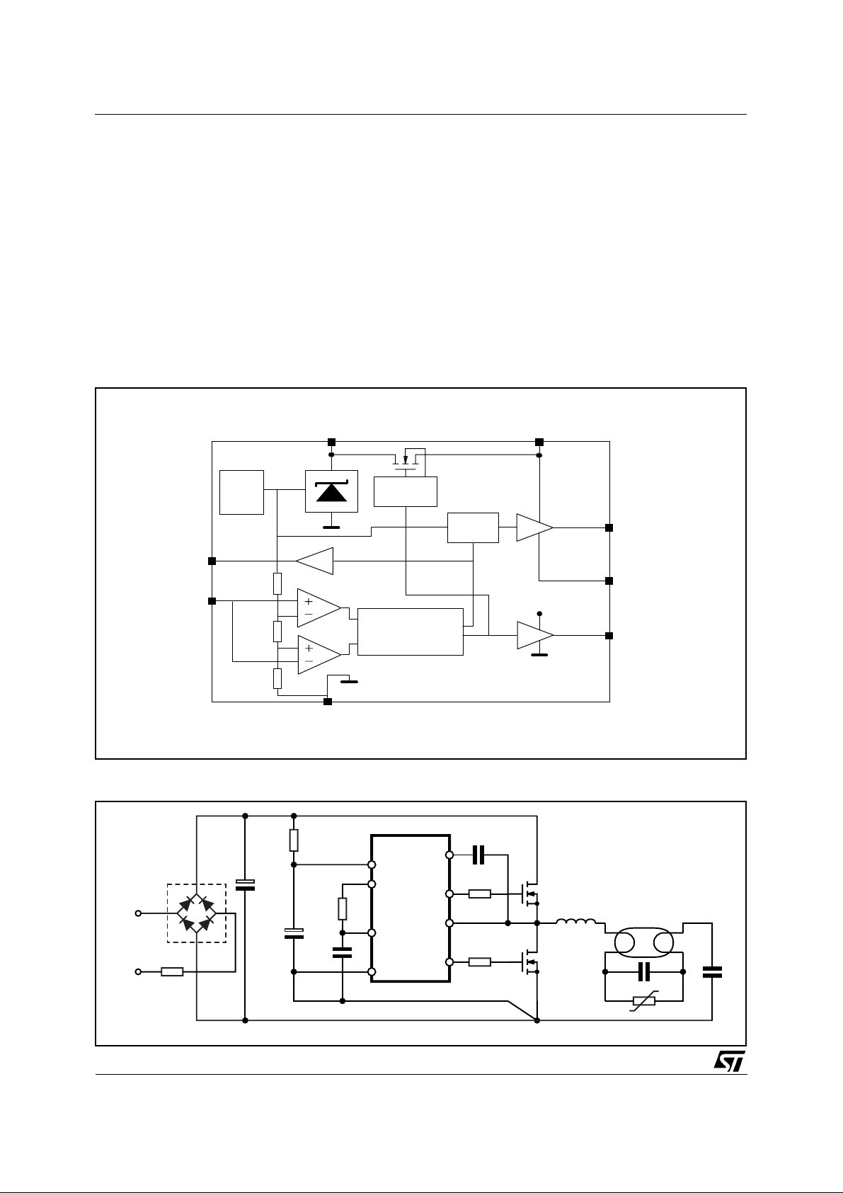
The L6569
The L6569 is able to directly control a symmetric
half bridge inverter of a fluorescent lamp ballast,
or a low voltage halogen lamp transformer.Two
270mA buffers drive the inverter MOSFETs in
complementary fashion with a 1.25µs built-in
dead time to prevent cross conduction. The buffer
for the upper Mosfet is driven through a 600V
level shifter realized in BCD off line technology.
The oscil lator, simil ar to a CMOS 555 timer, ope rates fr om 25 to 150 kHz wi th a +/-5% maximu m
tolerance. The in ternal 15V shunt regulator has a
9V Unde r Volt age Lock Ou t with an 1V hysteres is,
Figure 3: Block diagram of the L6569.
VS
UVLO
CHARGE
PUMP
RF
CF
LOGIC CONTROL
with DEAD TIME
and the circui t req uires o nly 150 µA at power up.
The L6569 integrates a high voltage Lateral
DMOS transistor in place of the usual external diode [2] to charge the bootstrap capacitor for the
upper buffer. Figure 5 shows DMOS operating as
a synchronous rectifier.
The applications
The primary application for the L6569 is the Compact Fluorescent Lamp. With the oscillator, the
supply and the Mosfet drivers it is the core of the
application, and designers can customize the circuit to their requirements.
BOOT
LEVEL
SHIFTER
HIGH
SIDE
DRIVER
HVG
OUT
LVG
LOW
SIDE
DRIVER
GND
Figure 4: Basic application diagram using the L6569 and two STD4NK50Z MOSFETs.
100nF
22Ω
STD4NK50Z
22Ω
D02IN1385
2/14
AC LINE
180KΩ
10µF
10µF
10KΩ
1nF
L6569
LAMP
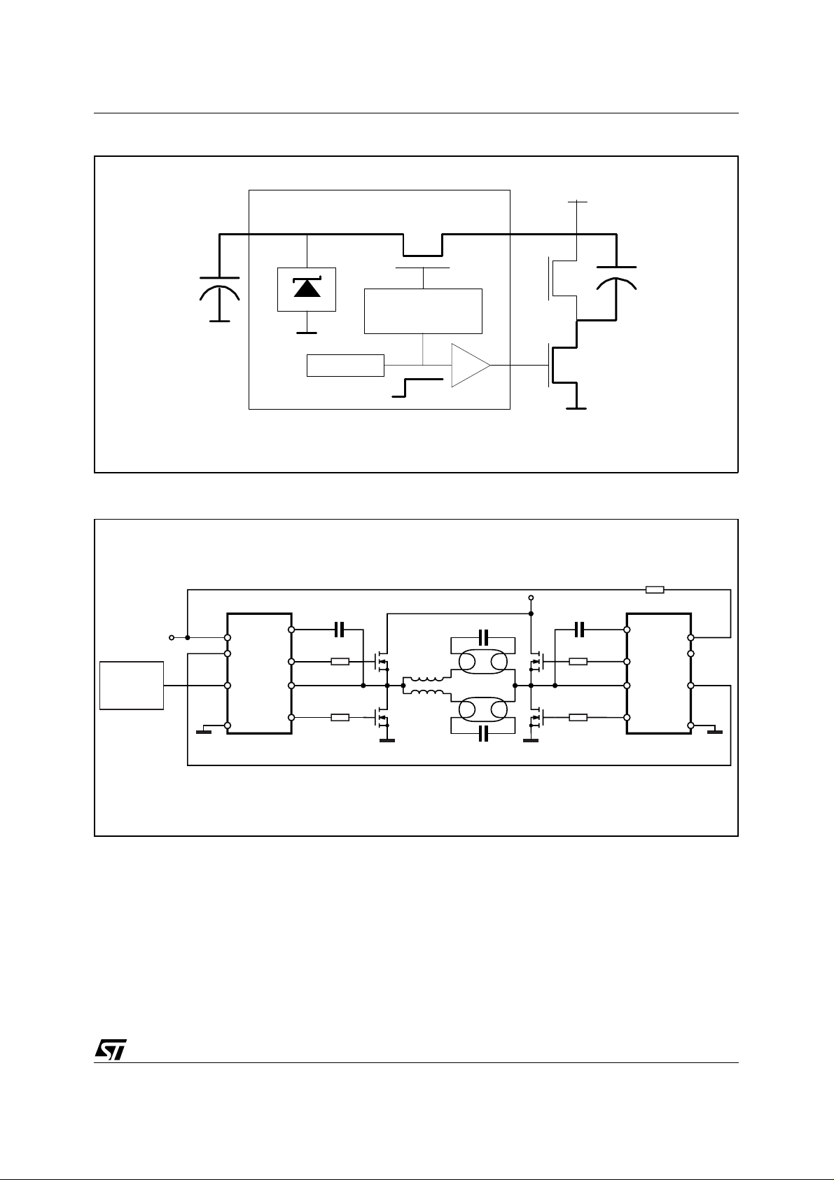
Figure 5: Bootstrap capacitor charge.
AN880 APPLICATION NOTE
15.6 V
600V 120
CHARGE PUM P CIRCUIT
LOGIC
ON
Ω
L6569
Figure 6: Basic diagram for 2x10⁵ W lamp ballast in full bridge configuration.
HV
100nF
BOOT
HVG
OUT
LVG
47
47
EXTERNAL
OSCILLATOR
V
V
S
RF
CF
GND
S
L6569
100nF
47
47
ON
BOOT
HVG
OUT
LVG
L6569
V
S
RF
CF
GND
D02IN1386
Typical industrial TL ballasts requires complex
control with dimming or automation interface.
Here the L6569 is a driver between the power
and control blocks. To use it with an external oscillator, pin CF is used as an 0-12V logic input,
and the L6569 becomes a high voltage buffer.
Applications with power above 150W require a full
bridge inverter. Figure 6 shows how two L6569
drive such a MOSFET bridge. If no external control is required, t he fir st L6569 m aster can control
the switching with its oscillator, and synchronizes
the other driver as (slave).
STB9NK50Z
The L6569 start up
Two versions of the L6569 are available with different start up characteristics. The L6569 drives
the lower MOSFET ON at power-up until the supply voltage reaches the Under Voltage Lock Out.
The bootstrap capacitor is precharged to 4.6V
and both the lower and the upper MOSFETs will
switch immediately with the oscillator. This is intended for inverters which use only one DC blocking capacitor connected to the power ground, as
shown on figure 4 for CFL ballast.
3/14

AN880 APPLICATION NOTE
The L6569A holds both MOSFETs OFF until the
Under Voltage Lock Out is reached. This is intended for inverters using 2 decoupling capacitors
in half bridge as shown on figure 12. The inverter
is totally off, so that the voltage at the capacitors
center node is not unbalanced by the leakage
path during power on.
CONSIDERATIONS ON THE L6569 ENVIRONMENT
To illustrate the benefits of the L6569 in t he CFL
applications, a demonstration board was developed to supply Sylvania 18W DULUX lamp (ref:
CF18DT/E). The following chapters summarize
the application considerations applied in t his design. The schematic, lay out and components list
are shown in appendix A.
Symmetric half bridge operation
To supply a fluorescent lamp, the ballast has to
achieve 3 functions: pre heat, ignition, and normal
lamp operation. The serial resonance occurs between the choke and the capacitor in parallel with
the lamp. The choice of these components determines the lamp ignition voltage a nd the nominal
lamp current.
Since the inverter using the L6569 and MOSFETs
can operate at a higher frequency than conventional solutions, the size of the passive components will be reduced. Such inverter can operate
up to 150 kHz in ZVS mode, and the switching
losses of the power transistors only limits t he frequency. In new design this frequency should be
set between 50 and 100 kHz. For instance with
an 18W lamp, a frequency increase from 33 to 50
kHz will lead to a 40% reduction of the choke
size.
To operate in Zero V oltage Switching (ZVS), the
switching frequency is higher than the resonant
frequency. All operation phases of the ballast ar e
secure in this mode. When the bootstrap transistor is conducting, no pulse c urrent will flow from
pin BOOT to pin V
, as it might happen in Zero
S
Current Switching. The bootstrap transistor remains in its Safe Operating Area, and its dissipation is negligible.
The MOSF ET dri ve
The ZVS drive technique requires only a fast turn
off capability as shown on f igure 2, and the transistor buffers are designed with a stronger sink
current. The two MOSFET buffers of the L6569
can sink a 400 mA peak current on capacitive
load. Typically these buffers can drive any MOSFETs in TO220 package.
Figure 7 shows an example with the STP8NA50
that has an 0.85 Ω resistance R
DS-ON
.
Figure 7: Cur re nt and voltage of the STP8NA50
MOSFET at turn off with the L6569.
T
= 245 ns ,Tc = 95 ns, E = 93 µJ
GD
@ Tj = 50°C, RG = 22 Ω.
GD
T
D
I
GS
V
D
V
50 ns/dv ; 1 A/dv ; 5 V/dv ; 50V/dv
Tc
GND
GND
GND
The built-in dead time circuit acts whe n a MOSFET turns off, delaying the turn on of the opposite
transistor for 1.25 µs. The voltage V
between
OUT
the 2 MOSFETs must switch within the minimum
dead time (0.85 µs), as shown on figure 8, to
avoid bridge cross conductions and transistors
overheat.
Figure 8: STD3NA50 MOSFET turn off when
driven by the L6569. T
D
T
I
D
C
T
GD
T
200 ns/dv ; 50 V/dv ; 0.1 A/dv
C
+ T
LVG
RF
GD
V
< T
DS
D
GND
GND
GND
The MOSFET voltage selection
Since the ballast is connected to the ac mains, it
must handle any spurious voltage spikes. When
the front end RFI filter and t he clamping device,
such as a varistor, absorbes totally the spike energy, MOSFETs can have the same 600V minimum breakdown voltage BV
as the L6569.
DSS
Otherwise when the upper MOSFET is on, the residual default may be applied to the L6569. Although the pin OUT breakdown voltage is higher
than 600V, it has a poor avalanche robustness.
Therefore the lower MOSFET protects the driver
by having a lower BV
mum BV
up to 500V will achieve safely this
DSS
. A MOSFET with a mini-
DSS
task.
4/14
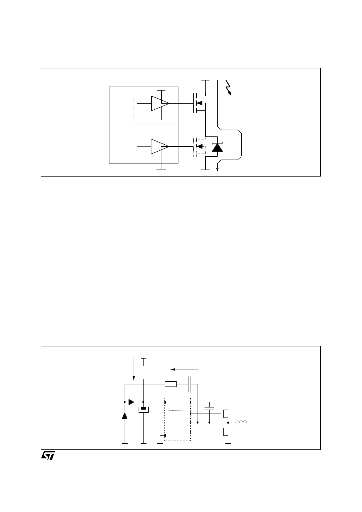
Figure 9. L6569 driver protection against voltage spikes.
AN880 APPLICATION NOTE
OUT
BV
> 600V
15V
L6569
The auxiliary supply of the converter
The circuit consumption is defined by the MOS-
H.V.+
ON
V
OUT
OFF
mA, a secondary winding on the resonant choke
is an easy supply alternative.
FETs gate charge, the I. C. consumption, the oscillator, and the shunt regulator. Several circuits
are possible.
In many applications a snubber i s used to reduce
the dissipation in the MOSFETs. When this snubber is used in conjunction with a start up resistor
in Figure 10), a non dissipative supply is
(R
S
achieved almost for free.
At start up t he I. C. i s co ns uming 150 µA, and the r e-
fore only a small supply resistor is required. During
operat ion the capacitor provides the supply current.
To avoid cross conduction, the capacitance is limited by the dri ver de ad tim e T
. Henc e the capaci-
D
tive supply current IC is also limited.For a CFL ballast this circuit easily supplies the required
operat ing c ur rent . Usi ng a CF18 DT lamp ( I
> 230
L
The ballast shutdown
The L6569 allows several ways (see figg. 11, 12
and 13) to shutdown the ballast [4]: by acting on
the C
input oscillator pin to turn off the upper
F
MOSFET or by acting on the VS supply pin with
the Under Voltage Lock Out.
Acting on C
(Fig. 11) a limiting resistor RL has to
F
be used, and it has to be: RL ⋅ CF > 1µs.
When the shutdown is realized acting on Vs pin,
(see fig. 12) a limiting resistor Rs must be used to
slow down the discharge of the supply filter Cs.
The constant time of the discharge must be
greater than 10 periods of the switching frequency:
mA) the required capacitance is 470 pF on 230 Vac
line. At 50 kHz the average capacitive current is 6
mA, as described in appendix B.
When the required driver current is higher than 10
Connecting the CF pin to ground GND stops the
oscillator, and the lower MOSFET will remain ON.
Therefore the bootstrap capacitor remains
Figure 10: Non dissipative auxiliary supply using the transistor snubber.
I
10
≥
R
S
⋅ f
C
s
sw
1mA WHEN STARTING
220k
Rs
Cs
Ω
6 mA WHEN 50 kHz SWITCHING
C
470 pF
310 V
bootstrap
circuit
L6569
5/14

AN880 APPLICATION NOTE
charged and the circuit can restart immediately.
This method is suitable when the inverter uses
only one DC blocking capacitor c onnected to the
power ground, as used on figure 11 for Compact
Fluorescent Lamp. Pulling the V
voltage below
S
the UVLO turns off the oscillator and gives the
same bridge configuration.
For the L6569A, discharging the V
supply below
S
the UVLO turns off bot h MOSFETs. An SCR like
the X0202MA may be used for the reset function.
If the current flowing through the supply resistor is
Figure 11: L6569 shutdown through the C
oscillator pin.
F
L 6569
R
R
F
L
C
F
higher than the SCR holding current (see figure
12), the SCR will remain on and the two MOSFETs off. Removing power or commutating the
SCR allows a new start up [4].
Otherwise a disable circuitry that turns off the two
MOSFETs (see figure13), can achieve the shutdown function. Compared to the SCR solution,
the shutdown is immediate and the inverter can
restart on the disable order.
ON
Figure 12: Shutdown with a thyristor & a serial resistor to slow down the supply voltage decay.
L 6569A
C
Rs
R
OFF
R
shutdown
OFF
Figure 13: L6569 disable circuitry with both MOSFETs off.
H.V.
22
V
IN
DISABLE
HCF4011
5.6k
Vs
VS BOOT
HVG
RF
OUT
CF
LVGGND
100nF
200
200
L6569
W
4.7 k
BC327
6/14

AN880 APPLICATION NOTE
THE LAMP SEEN BY THE ELECTRONIC DESIGNER
The lamp equivalent impedance
The compact fluorescent lamps are specified at
25 kHz (IEC 929). The MOSFETs and the L6569
allow to increase the switching frequency, but the
sensitivity of the lamp to the frequency needs to
be analyzed.
A few samples of the CF18DT/E lamp were
tested by varying the frequency and the current of
the lamp. The figure 14 shows the lamp impedance versus its current as it varies from 0.1A to
0.23A with 5 frequencies from 25 to 150 kHz
= 25°C).
(T
AMB
Figure 14: Variation of the lamp impedance
versus its cu rren t for seve r a l
switching frequencies.
R lamp (Ohms)
1200
1000
800
600
400
200
25 kHz
50 kHz
100 kHz
150 kHz
The preheat
Preheat techniques are used in CFL ballasts to
reduce the ignition lamp voltage. During this
phase the lamp is characterized by a high impedance that forces the electrical conduction through
the preheat filaments. These filaments initially
have a low resistance that will increase by 5 times
during the preheat. The preheat typically lasts
from 400 ms to 1 s, and is achieved by controlling
either the current or the voltage of the filaments.
For a current control the filaments are in series
with the resonant network as shown on figure
16a. When the inverter frequency is constant, a
positive temperature coefficient thermistor (PTC)
in parallel with the lamp achieves the t ask by adjusting both the filament current and the preheat
duration. The board uses a 150Ω PTC with two
8.2 nF capacitors. The preheat lasts 0.8s and the
filament current is 0.45 Arms. The PTC is a cheap
device, but it is dissipative and works only once at
power-up.
Figure 16: Basic preheat current control diagram
(a); preheat filament energy curve (b)
0
0.05 0.1 0.15 0.2 0.25 0.3
I lamp (A)
From the tests the impedance appears insensitive
to the frequency for such lamps. The specified impedance might be valid for higher frequency operation. The relative lamp light output was measured as proposed in reference [5]. The light flux
increases slightly in that frequency range, but can
be considered constant.
Obviously the impedance is sensitive to the current with a negative coefficient, and the ballast
operates with a non linear impedance [6]. When
current is half the nominal one, the impedance is
2.6 times higher, and the voltage is only 25%
higher (see figure 15).
Figure 15: Variation of the average impedance
and voltage of the lamp
R (Ohms) U (V)
1200
900
600
300
0
0.05 0.1 0.15 0.2 0.25
I (A)
200
150
100
50
0
Rlamp
Vlamp
I
CTL
(A)
LAMP
E
If
E=R.I²
CTL
(B)
I
t
The preheat can be achieved with a filament voltage control. The filaments are supplied by two
auxiliary windings of the resonant choke as
shown figure 17a. During the preheat the L6569
frequency is increased, and the choke operates
7/14

AN880 APPLICATION NOTE
as a transformer supplying the voltage to the filaments. Only few components are added around
the L6569 (see figure 18), and the control of the
preheat energy is less sensitive to the preheat duration and the inverter frequency (see figure 17b).
Figure 17: Basic preheat voltage control diagram (a); preheat filament energy curve (b)
The start up initialization
The initial conditions of t he power switching start
up requires care; especially if the resonant and
switching frequencies are close to each other.
The resonant network is not loaded and the full
(A)
CTL
V
LAMP
E
Vf
CTL
V
(B)
E=V²/R
t
Figure 18: Double frequency control for the L6569 with programmed frequency and duration.
1_Vs
2_RF
F
R
3_CF
R
C
F
L6569
C
8/14
C
F_ST

AN880 APPLICATION NOTE
line voltage VDC is applied when the oscillator
starts. The ballast has to start directly with its
nominal conditions to remove any transient oscillation. Hence the operation runs in ZVS mode
with no spurious lamp ignition. Th is situation does
not occur with the saturable transformer drive, because the saturation limits naturally the cur rent by
increasing the frequency.
In the example the resonant capacitors are preset to be compatible with the choke current rise
(see figure 19). The blocking capacitor is precharged to approximately half V
by 2 biasing
DC
resistors, and the lower Mosfet also discharges
the resonant capacitor to ground (see figure 20).
Therefore the blocking capacitor never goes
above 2/3 of the line voltage V
(250V rating),
DC
the operation is safe in ZVS mode. The L6569 is
here preferred to the L6569A, because the lower
Figure 19: Waveforms of the choke current and
the capacitor voltages in steady state
preheat.
IDEAL INITIAL TIME
I
I
GND
The lamp removal protection
Used in TL ballast, the lamp removal protection is
frequently also requested in the "plug-in" CFL ballast . Depending of the topology and the preheat
mode, the lamp removal behaves as:
- a noload resonant mode when the choke and
the capacitor are still connected to the inverter ; a required overcurrent protection increases the frequency to reduce the current;
- an open circuit mode when the lamp filaments
are inserted in the resonant circuit.
When the circuit is open, the choke is not supplied. The MOSFETs turn off slowly generating
bridge cross conduction, and undesirable dissipation losses (see figure 21). The detection stops
the switching to eliminate the cross conduction.
Figure 21: Drain current and voltage STP8NA50
MOSFET operating with noload.
ID = 2 A peak
V
D
V
GS
GND
I
D
BI
V
5 µs/dv ; 50 V/dv ; 0.5 A/dv
B
V
GND
10 0 n s/d v ; 5 0 V/d v ; 5 V/dv ; 1 A/d v
Mosfet is on at power-up.
Figure 20: Configuration of the resonant network during the initialization of the driver.
VS<UVLO
2.4 mH
I
I
ON
L6569
2 x 180 k
V
B
Ω
100 nF
V
GND
GND
BI
4nF
9/14

AN880 APPLICATION NOTE
Figure 22: Open load detection example.
L6569
3_CF
4_GND
LAMP
18V
Several ways can achieve the protection task.
First it can be done by sensing the resonant current through a MOSFET source resistor or a secondary winding on the choke. The switching is
stopped when a large current reduction is detected by analog means.
A logic circuit can also detect t he presence of t he
lamp filaments. One end of a filament is always
connected to a fixed voltage . If the other end of
the filament is connected through a high impedance resistor to another volt age, the absence of
the filament can be easily detected by monitori ng
the resistor voltage change as shown on figure
22.
CONCLUSION
The foregoing note shows how high voltage drivers, like the L6569, simplify the design of the
lamp ballast. These devices includes all the circuitry to drive MOSFETs in half bridge inverter.
Since the optimized switching frequency increases above 50 kHz with a low tolerance, the
size of the passive resonant components is re-
10.R
100.R
11.R
10.R
duced, and the ballast becomes cheaper.With its
supply and its oscillator the L6569 is versatile,
and its flexibility permits to design any improved
power control.
BIBLIOGRAPHY
[1]: AN 527 "Electronic fluorescent lamp ballast"
A.Vitanza, R.Scollo, SGS-THOMSON
[2]: Smart Power ICs, Chapter 8, High voltage integrated circuits for off-line power applications.
C.Diazzi, SGS-THOMSON
[3]: AN 512 "Characteristics of power semiconductors" JM Peter, SGS -T H O M SO N
[4] : "The L6569 half bridge driver: the shutdown
function"
[5] : "Compatibility test of dimming electronic ballasts used in daylighting and environment controls", A.Buddenberg, Rensselaer Polytechnic Institute
[6]: "PSpice High Frequency Dynamic Fluorescent Lamp Model", Bryce Hesterman, APEC’96,
p.641
10/14

AN880 APPLICATION NOTE
APPENDIX A: CF L DEMONSTRATION BOARD
WITH THE L6569
A demonstration board was developed as an example for Compact Fluorescent Lamp ballast. It is
optimised for a CF18DT/E/830 18W lamp from
Osram-Sylvania. Using the L6569 the circuit
achieves preheat, ignition and normal lamp operation. The power transistors are two STD3NA50
500V-3Ω MOSFETs in I-PACK package.
Board description
The three sections of the board are an AC input
rectifier, the half bridge inv erter, and the resonant
ballast. By changing the connection on the input
mains, the ballast can operate either on 120 Vac
mains with a voltage doubler rectification, or on
230 Vac mains with a full wave rectification. The
input resistor R
limits the initial inrush current
1
charging the bulk capacitors. The L6569 operates
with a single 50 kHz switching frequency programmed by R
and C1. Two fast diodes D2 & D
4
synchronize the oscillator to keep the switching in
ZVS mode. The control circuit requires 4.5 mA to
supply the I.C., the MOS gate drives, and the oscillator. Its supply delivers at least 6.5 mA as described in appendix B. The start up resistor also
balances the voltage across the two bulk capacitors.
Figure 23. CFL ballast diagram for a 18W
CFD18T/E lamp with 120/230 Vac inputs.
The resonant ballast
The value of the choke (L
tors (C
& C8) in parallel with the lamp determine
7
) and the two capaci-
1
the lamp ignition voltage and the nominal lamp
current. During the ignition the lamp impedance is
essentially infinite, and the filaments resistance is
only the serial load. To generate the ignition voltage, the switching frequency is set close to the
resonance frequency. In normal operation the
choke resonates with the capacitors C
(parallel loading), but also with the decoupling capacitor C
(serial loading). The current mode pre-
6
heat uses a 150Ω Positive Temperature Coefficient thermistor. Inserted in the capacitive series
& C8), the PTC produces a 0.45 Arms fila-
(C
7
ment current during the initial 0.8 s (reference:
307C1253BHEAB from CERA-MITE).
Basic ballast electrical characteristics
Input voltage: 120 or 230 Vac by input connections change
3
Switching frequency: 50kHz
Average dc line voltage range: Vdc from 260 to 355
Nominal supply current: 0.17A rms @ 310 Vdc
Nominal output power: 17W
Minimum ignition voltage: 700V peak @ 260 Vdc
Nominal preheat current: 0.45 Arms during 0.8s
@ 310 Vdc
& C
7
8
Figure 23.
4 x 1N4006
D7 D4
220V
N
R1 15 1W
110V
R8
120K
1/2W
D5D6
L1=2.4mH core TH LCC E2006-B4 Ref also VOGH 575 0409200 2.4mH
C7-C8=PS8n2J H3 630-2A TH
(*) Polypropylene, Capacitors 630V rated V
C5
47µF
250V
C2
47µF
250V
R5 100K
1/2W
C3
4.7µF
25V
R4
27K
1/4W
D8
1N4148
ZPD 18V
V
S
RF
L6569
CF
C1
560pF
50V
D1
L
C9 470pF 630V
R6 47 1/4W
BOOT
HVG
OUT
LVG
GND
(*)
C4100nF 50V
R2 22 1/4W
R3 22 1/4W
D96IN419C
R10 10K
1/4W
Q1
STD4NK50
Q2
STD4NK50
R7
180K
1/4W
BYW100-100
D2
D3 BYW100-100
R9
180K
1/4W
L1=2.4mH
C6
100nF
250V
CFL LAMP
SYLVANIA DELUX T/E 18W
C7
8.2nF
630V
(*)
C8
8.2nF
630V
(*)
RV1
PTC 150
350V
11/14

AN880 APPLICATION NOTE
Figure 24: PCB Layout of the board.
Comp.
Side
Copper
Side
Figure 25: PCB component placement diagram.
The resonant choke
The inductance of the choke is 2.4 mH with a
minimum saturation current of 0.65 A. In the practical example it has been done with:
Core: Thomson LCC E2006 material B4;
Air gap: 2 spacers of 0.4 mm each (total 0.8 mm);
AL = 75 nH;
Bobbin: HC2006BA-06;
Number of turns: 175;
Measured saturation current: 1 A peak @ 25 °C;
Customization of the board
Some flexibility is added to the board to extend its
evaluation. The MOSFETs have two foot prints to
mount either I-PAK or TO220 packages. And two
choke footprints are also avalaible for E1905A
and E2006A magnetic cores.
12/14

AN880 APPLICATION NOTE
APPENDIX B: Rating of the capacitive supply
with the L6569 driver
The supply is made with the snubber and a start
up resistor R
.
S
A snubber circuit is used to minimize the MOSFETs dissipation. It also achieves a non dissipative supply as shown on figure 10.
The MOSFETs gate charge, the driver consumption, the oscillator, and the shunt regulator, define
the circuit consumption. We can estimate this
current is I
:
S AV
> 2 ⋅ IG + IQS + I
I
SAV
= 2 ⋅ Q
⋅ fsw + IQS +
G
+ I
OSC
V
S
RF ⋅ 2
REG
+ I
=
REG
Where QG the MOSFET gate charge
I
V
R
the driver supply current
QS
the supply voltage
S
the oscillator resistor and VS the driver
F
supply voltage
I
When VS is lower than the UVLO threshold U
the shunt regulator current.
REG
UVLO
, the
driver is only consuming. Its current must be minimal to reduce the dissipation of the resistor R
The L6569 has a 150 µA start up current, and the
maximum resistance is 2MΩ for a 230Vac line application.
We can also reduce the resistor value to get a
faster start up time T
T
.
S
S
⋅ C
⋅ U
S
UVLO
V
DC
R
=
S
Where CS is the supply capacitor, and VDC the
line voltage.
When the timer oscillates, the capacitor C sup-
plies the lamp current during the lower MOS turn
off. To avoid any cross conduction its capacitance
is limited by the driver dead time T
26). Hence the capacitive supply current I
limited.
I
= C ⋅ VDC ⋅ FSW < IL ⋅ TD ⋅ F
CAV
C <
TD ⋅ I
V
L
DC
Where IL is the peak lamp current, and F
switching frequency.
For a ballast such as a CFL one this circuit supplies easily the required current. For instance with
a CF18DT lamp ( I
> 230 mA) the capacitor is
L
1nF on 120Vac line, 470 pF on 230 Vac line. At
50 kHz the average capacitive current is 6 mA in
both cases.
Figure 26: Cross conduction of the snubber
capacitor with the upper MOSFET:
capacitor current and voltage
waveforms.
.
S
GND
GND
GND
200 ns/dv ; 50 V/dv ; 0.1 A/dv
D
T
(see figure
D
is also
C
SW
SW
V
+ V
HVG
I
C
RF
the
OUT
13/14

AN880 APPLICATION NOTE
Information furnished is bel ieved to be accurate and reliable. Howev er, STM icroele ctronics ass umes no respons ibilit y for the consequence s
of use of such i nformation nor for any i nfringement of patents or ot her rights of third parties which may result from its use. No l icense is
granted by impli cation or otherwis e under any patent or patent righ ts of STMicroelectro nics. Specification mentioned i n this publication are
subject to change withou t notice. This publica tion supersed es and replac es all informat ion previousl y supplied. STMic roelectro nics products
are not authorized for use as critical components in life support devices or systems without express written approval of STMicroelectronics.
The ST logo is a registered trademark of STMicroelectronics
© 2003 STMicroelectronics – Printed in Italy – All Rights Reserved
STMicroelectronics GROUP OF COMPANIES
Australia - Brazil - Canada - China - Finland - France - Germany - Hong Kong - India - Israel - Italy - Japan - Malaysia - Malta - Morocco -
Singapore - Spain - Sweden - Switzerland - United Kingdom - United States.
http://www.st.com
14/14
 Loading...