

Page 1

AN836
APPLICATION NOTE
LOW FORWARD VOLTAGE SCHOTTKY DIODE
INTRODUCTION
In power supplies, the major portion of power losses is due to output rectifiers. The impact of these losses
on the efficiency can be expressed by:
IOUT()
V
η
η :efficiency drop due to the diodes.
V
V
This formula shows that the influence of the forward voltage increases when the output voltage of the power supply decreases.
This parameter becomes very important for the new standard of 3.3V output voltage. Another key parameter is the leakage current which we have to take into account to develop high efficiency low forward voltage drop Schottky with the best trade-off.
F
-------------------------- -=
V
OUT
F(IOUT)
OUT
:voltage drop at the output current
(IOUT) of the converter.
:output voltage of the converter.
TRADE-OFF
The 3 most important application characteristics of a Schottky are:
– forward voltage
– reverse leakage current
– reverse blocking voltage
Generally for a given application, the first step is to fix the reverse blocking voltage. We then study the
best trade-off (choice of a metal barrier) between the forward voltage and the leakage current.
A decrease of the forward voltage increases the efficiency of the converter but increases at the same time
the leakage current and limits operating range where we can keep the reverse losses under control. In the
datasheet this range is defined by Tj max.
To define the best trade off of a low forward voltage schottky we have to take into account its application
condition. STMicroelectronics has developed two families of low forward voltage Schottky well suitable to
two applications: the OR-ing Schottky and Schottky for 3.3V output power supply secondary.
SCHOTTKY DIODES FOR 3.3V SWITCHED MODE POWER SUPPLY
When a Schottky works in a switched mode power supply (forward, flyback,...), it sees during the same
switching period conduction losses and reverse losses.
In these configurations the trade-off between the forward voltage and the leakage current has to be chosen to have the best efficiency with a sufficient safety margin. This is to keep the reverse losses under
control (Tj max = 125°C).
REV. 2
1/5May 2004
Page 2
AN836 APPLICATION NOTE
Table 1. Main Characteristics of Schottky
V
PART NUMBER PACKAGE Io
typ Max Max
AmVmVmA
STPS125U SOD6 1
390
(1)
STPS5L25B DPAK 5 310 350 175
STPS10L25D TO220AC 10 300 350 400
STPS15L25D/G D2PAK/TO220AC 15 300 350 640
STPS20L25CT TO220AB 2x10 300 350 400
STPS20L25CG D2PAK 2x10 300 350 400
Note: 1. Main characteristics of the 25V low VF Schottky
OR-ING SCHOTTKY
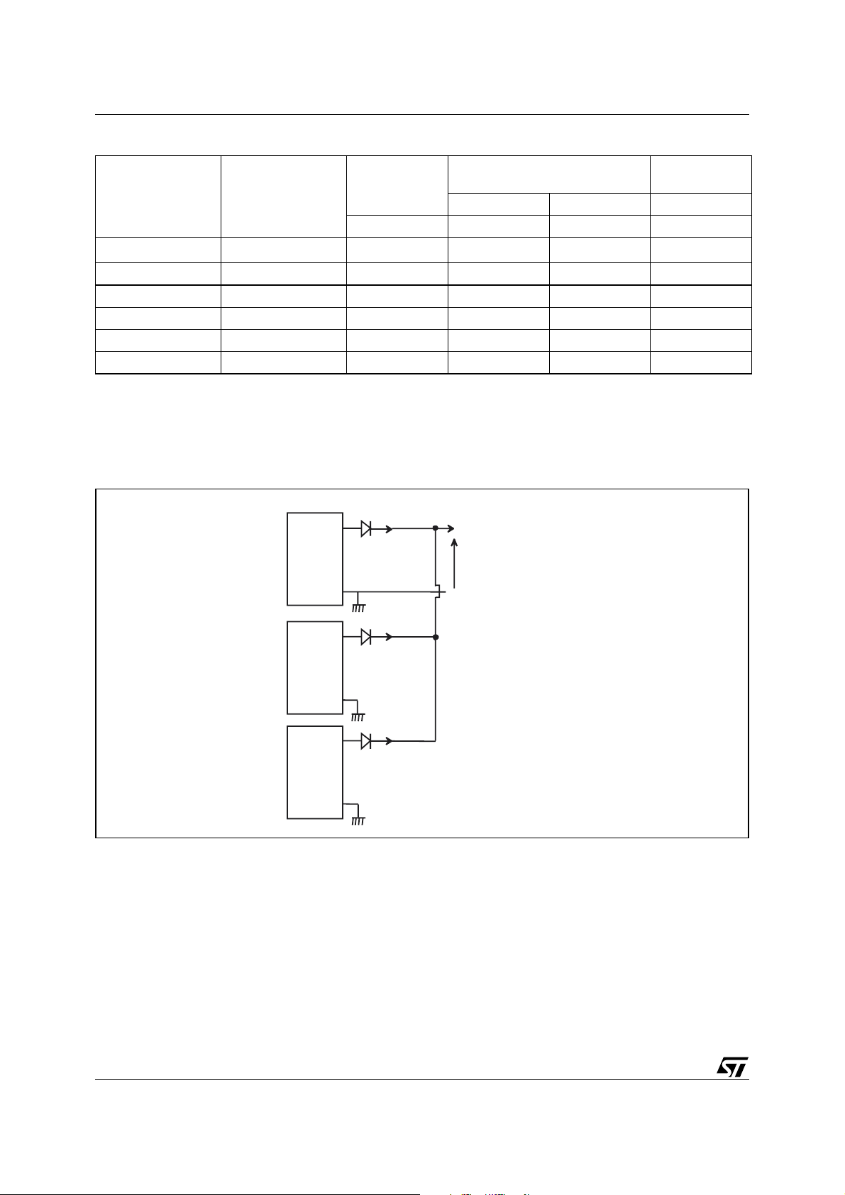
To increase system reliability, power supplies are sometimes connected in parallel (Fig.1).
Figure 1. OR-ing Schottky in redundant power supply
F
(Io,125°C)
460
(125°C, 25V)
(1)
I
R
(1)
2
POWER
SUPPLY
1
POWER
SUPPLY
2
POWER
SUPPLY
n
I
OUT/n
I
OUT/n
I
OUT/n
I
OUT
V
OUT
3.3V, 5V or 12V
The Schottky diodes are connected in series with the output of each power supply. In the steady state a
continuous current (I
T/n) flows in each Schottky. Obviously in this case there are no reverse losses.
OU
When a power supply fails, the corresponding ORING diodes ceases to carry current and the system output voltage is not disturbed. The OR-ing diode then sees the reverse voltage V
OUT
.
In this application the most critical parameter is the forward voltage drop in order to maintain the best efficiency of the system. A breakdown voltage of 10V is sufficient for output voltage of 5V and 3.3.V.
The trade-off has been chosen to obtain a low forward voltage. In this application we can accept a high
leakage current because when the diode is blocked the reapplied voltage is low (3.3V or 5V), the junction
temperature is also low because there are only reverse losses. So it’s easy to keep reverse losses under
control.
2/5
Page 3

AN836 APPLICATION NOTE
Table 2 gives the main characteristics of the 10V and 15V schottky.
Table 2. Main Characteristics of 10V and 15V Schottky
V
PART NUMBER PACKAGE Io
F
(Io,105°C)
typ Max Max
AmVmVA
STPS15L10D TO220AC 15
270 320 0.42
STPS80L10TV ISOTOP 2x40 270 320 1.2
STPS20L15D TO220AC 20
STPS40L15CW TO247 2x20
Note: 1. I=19A
2. VR=12V
3. I=19A per diode
0.31
0.31
(1)
(3)
0.36
0.35
(1)
(3)
CONCLUSION
The equilibrium between efficiency and safety margin against thermal runaway has been best solved with
25V, 15V and 10V Power Schottky diodes. One being suitable for 3.3V supplies and the other for the redundant Powers supplies.
Moreover, the inclusion of Power Factor correction will significantly change the choice of the Schottky diode for the secondary Power supply rectification.
With PFC, the reapplied voltage across the output rectifiers will be lower. For example we can consider
using 25V Schottky in a 5V forward converter, whereas today a 45V Schottky diode is needed.
I
R
(100°C, 10V)
(2)
0.55
(2)
0.55
Per diode
3/5
Page 4

AN836 APPLICATION NOTE
REVISION HISTORY
Table 3. Revision History
Date Revision Description of Changes
August-1995 1 First Issue
10-May-2004 2 Stylesheet update. No content change.
4/5
Page 5

AN836 APPLICATION NOTE
Information furnished is believed to be accurate and reliable. However, STMicroelectronics assumes no responsibility for the consequences
of use of such information nor for any infringement of patents or other rights of third parties which may result from its use. No license is granted
by implication or otherwise under any patent or patent rights of STMicroelectronics. Specifications mentioned in this publication are subject
to change without notice. This publication supersedes and replaces all information previously supplied. STMicroelectronics products are not
authorized for use as critical components in life support devices or systems without express written approval of STMicroelectronics.
The ST logo is a registered trademark of STMicroelectronics.
All other names are the property of their respective owners
© 2004 STMicroelectronics - All rights reserved
STMicroelectronics GROUP OF COMPANIES
Australia - Belgium - Brazil - Canada - China - Czech Republic - Finland - France - Germany - Hong Kong - India - Israel - Italy - Japan -
Malaysia - Malta - Morocco - Singapore - Spain - Sweden - Switzerland - United Kingdom - United States
www.st.com
5/5
 Loading...