

Page 1

AN828
®
1500W - 440V POWER FACTOR CORRECTOR
The application here described has been tailored
to supply a three phase inverter for motion control (see fig.1). To reduce the current in the
switches of the inverter, the output voltage of the
power factor has been held quite high.
The target specification of the PFC application is:
Mains supply Vin(rms) = 220Vac ±20%
(f = 50/60Hz)
Output Voltage Vout = 440Vdc
Output Power Pout = 1500W
A switching frequency of 60kHz has been chosen
as a good compromise between r equirements of
small size magnetics and low switching losses.
For this application a full isolated ISOTOP(TM)
STE30NA50-DK has been used.
This module is especially intended for boost applications and consists off the integration of a low
RDS/500V Mosfet with a TURBOSWITCH(TM) diode.
The use of the module allows a compact and ef-
APPLICATION NOTE
PREREGULATOR
fective solution in terms of layout and power dissipation. The output stage of the L4981A/B is capable of driving directly the module without the
aid of a buffer stage. The L4981A controller is
supplied by the auxiliary of the boost inductor, a
Graetz bridge and a simple resistor for the startup phase. The Output capacitor filter has been realized connecting in parallel four tap in "series"
configuration. This solution allows the use standard parts, in terms of the rat ed voltage, resulting
easier to be implemented in comparison with a
"single" configuration. To be noted that the high
frequency filter (C1 + C2) has been split in two
parts. In this way it is possible to held a low value
capacitor (C2) connected to the output of the rectifier bridge, minimising the harmonic distortion
(introduced by the rectified DC contents). On the
other hand, the capacitor (C1) connected to the
AC side of the bridge, performs most of the high
frequency filter function without introducing DC
content.
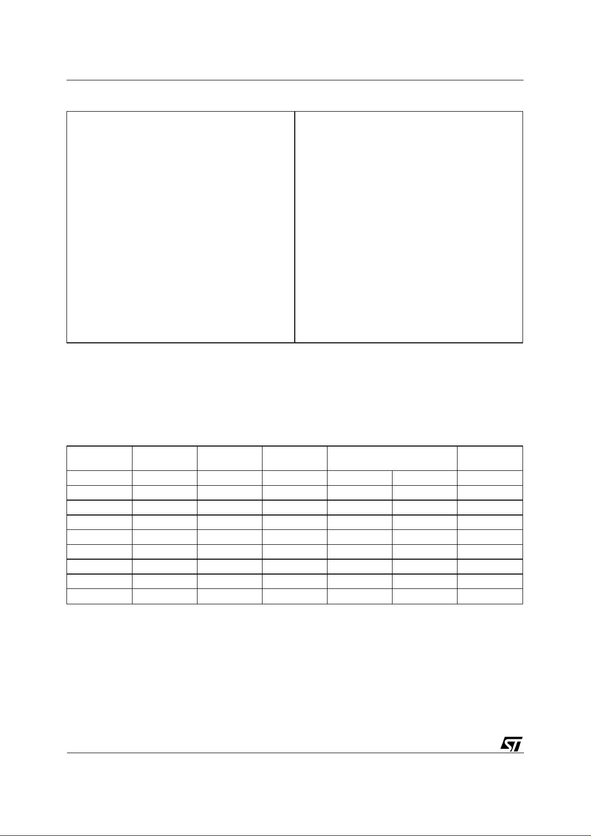
The schematic circuit is shown in fig.1
Figure 1: Schematic Diagram
C2
220nF
BRIDGE
KBPC25-04
R1
5.1K
1%
220
1%
R4
1M
4
1
7
6
11
R2
2.2µF
Vi
250V
176VAC/265V
FUSE
10A/250V
C1
+
-
AC
Transformer
Core: THOMSON - CSF GER55x28x25
Gap: 3.1mm for a total primary inductance of 440µH
Primary: 42 turns of 8x0.5mm (#24 AWG)
Secondary: 4 turns of #27 AWG (0.15mm)
75K
R3
1W
R8
3.9K
5%
R5
47
500mW
19
R6 100K
5%
RS 10mΩ
T
C3
330nF
3.9K
-
+
R9
5%
D2
4 x
1N4150
Dz 18V 500mW
C4 220µF 25V
L4981A
C5
105nF
C6 330nF
R10 120K 5%
13 14
1217 10189582
R7
C7
27K
10µF
1%
16V
R11 3.9K 5%
3
20
R12 15 5%
R13
1 5%
STE30NA50-DK
D3
1N4150
R14
820K
1%
R15
10K
1%
D95IN249C
R16
909K
1%
Rx
150K
Rx
150K
R17
10K
1%
4 x
470µF
315V
4 x
470µF
315V
+
Po=1500W
Vo=440V
-
Co
1µF
630V
October 2002
1/3
Page 2
AN828 APPLICATION NOTE
L4981A PARTS LIST
Boost inductor (T) L = 0.44mH
Core :Thomson - E 55x28x25
Gap = 3mm
Primary Turns = 42 (8 x 0.5mm)
Secondary Turns = 4 (0.15mm)
Co= 940µF = [(4 + 4) x 470µF/315V + 1µF/630V]
C1 = 2.2µF/250Vac
C2 = 220nF/630V
C3 = 330nF
C4 = 220µF/25V
C5 = 1.5nF
C6 = 330nF
C7 = 10µF
Power Switch = STE30NA50-DK
Input Bridge = KPBC25-04
D2 = 1N4150 (X 4)
D3 = 1N4150
Rs = 10mΩ /1W
R1 = 5.1kΩ /1%
R2 = 220Ω /1%
R3 = 75kΩ/1Ω
R4 = 1M
R5 = 47 /1/2Ω
R6 = 100kΩ
R7 = 27k /1%
R8 + R9 = 3.9kΩ
R10 = 120kΩ
R11 = 3.9kΩ
R12 + R13 = 15Ω
R14 = 820kΩ /1%
R15 = 10kΩ /1%
R16 = 909kΩ
R17 = 10kΩ
Table 1: Test Result.
Mains rms
(V)
176 451 509 0.998 2.0 1.9 94.2
176 444 937 0.999 1.4 1.3 94.0
176 438 1396 0.999 1.0 0.9 94.0
220 451 509 0.996 2.1 1.9 95.6
220 445 941 0.998 1.5 1.4 95.2
220 438 1396 0.999 1.0 0.9 95.3
260 452 511 0.993 2.5 1.9 95.1
260 446 945 0.997 1.4 1.3 96.4
260 439 1402 0.999 1.1 0.8 96.1
CONCLUSIONS
The evaluation has been done using the "A" version of the L4981 controller, without using additional features obtaining high performance results, in terms of efficiency and harmonic content.
Vout
(V)
Pout
(W)
Power
Factor
Harmonic Distortion (%)
THD AH3
Further improvements are possible using the additional features of the I. C. such as the LFF (pin
16) for the best control of the output voltage or
by the use of the B version to minimise the EMI
filter.
Efficiency
(%)
2/3
Page 3

AN828 APPLICATION NOTE
Information furnished is bel ieved to be accurate and reliable. Howev er, STM icroele ctronics ass umes no respons ibilit y for the consequence s
of use of such i nformation nor for any i nfringement of patents or ot her rights of third parties which may result from its use. No l icense is
granted by impli cation or otherwis e under any patent or patent righ ts of STMicroelectro nics. Specification mentioned i n this publication are
subject to change withou t notice. This publica tion supersed es and replac es all informat ion previousl y supplied. STMic roelectro nics products
are not authorized for use as critical components in life support devices or systems without express written approval of STMicroelectronics.
The ST logo is a registered trademark of STMicroelectronics
© 2002 STMicroelectronics – Printed in Italy – All Rights Reserved
STMicroelectronics GROUP OF COMPANIES
Australia - Brazil - Canada - China - Finland - France - Germany - Hong Kong - India - Israel - Italy - Japan - Malaysia - Malta - Morocco -
Singapore - Spain - Sweden - Switzerland - United Kingdom - United States.
http://www.st.com
3/3
 Loading...