


AN670
Application note
Oscillator selection for ST62
Introduction
The purpose of this note is to give indications on how to choose a resonator or a quartz
crystal in order to achieve reliable oscillation with the ST62 Microcontroller. This document
provides first the major resonator parameters useful for a design. It then proposes
measurement methods to ensure a safe oscillation.
October 2008 Rev 2 1/12
www.st.com

Contents AN670
Contents
1 Oscillation frequency . . . . . . . . . . . . . . . . . . . . . . . . . . . . . . . . . . . . . . . . 3
2 Oscillation conditions . . . . . . . . . . . . . . . . . . . . . . . . . . . . . . . . . . . . . . . . 4
2.1 Barkhausen criteria . . . . . . . . . . . . . . . . . . . . . . . . . . . . . . . . . . . . . . . . . . 4
2.2 Start-up . . . . . . . . . . . . . . . . . . . . . . . . . . . . . . . . . . . . . . . . . . . . . . . . . . . 4
2.3 Measurement of the loop gain (open loop) . . . . . . . . . . . . . . . . . . . . . . . . . 5
2.4 Frequency stability . . . . . . . . . . . . . . . . . . . . . . . . . . . . . . . . . . . . . . . . . . . 5
2.5 Start-up time . . . . . . . . . . . . . . . . . . . . . . . . . . . . . . . . . . . . . . . . . . . . . . . . 6
3 Conclusion . . . . . . . . . . . . . . . . . . . . . . . . . . . . . . . . . . . . . . . . . . . . . . . . . 7
Appendix A Test of a CSA Murata crystal resonator with an ST6210xx . . . . . . . 8
A.1 Choice of the network capacitances . . . . . . . . . . . . . . . . . . . . . . . . . . . . . . 8
A.2 Pseudo closed loop measurement . . . . . . . . . . . . . . . . . . . . . . . . . . . . . . . 8
A.3 Start-up time . . . . . . . . . . . . . . . . . . . . . . . . . . . . . . . . . . . . . . . . . . . . . . . . 8
A.4 Conclusion. . . . . . . . . . . . . . . . . . . . . . . . . . . . . . . . . . . . . . . . . . . . . . . . . . 8
Appendix B Calculation of the resonant frequency of ceramic resonator . . . . . 9
B.1 Equivalent circuit at the resonance frequency. . . . . . . . . . . . . . . . . . . . . . . 9
B.2 Transformation for simple calculation . . . . . . . . . . . . . . . . . . . . . . . . . . . . . 9
B.3 Resonant frequency . . . . . . . . . . . . . . . . . . . . . . . . . . . . . . . . . . . . . . . . . . 9
B.4 Note. . . . . . . . . . . . . . . . . . . . . . . . . . . . . . . . . . . . . . . . . . . . . . . . . . . . . . 10
4 Revision history . . . . . . . . . . . . . . . . . . . . . . . . . . . . . . . . . . . . . . . . . . . 11
2/12
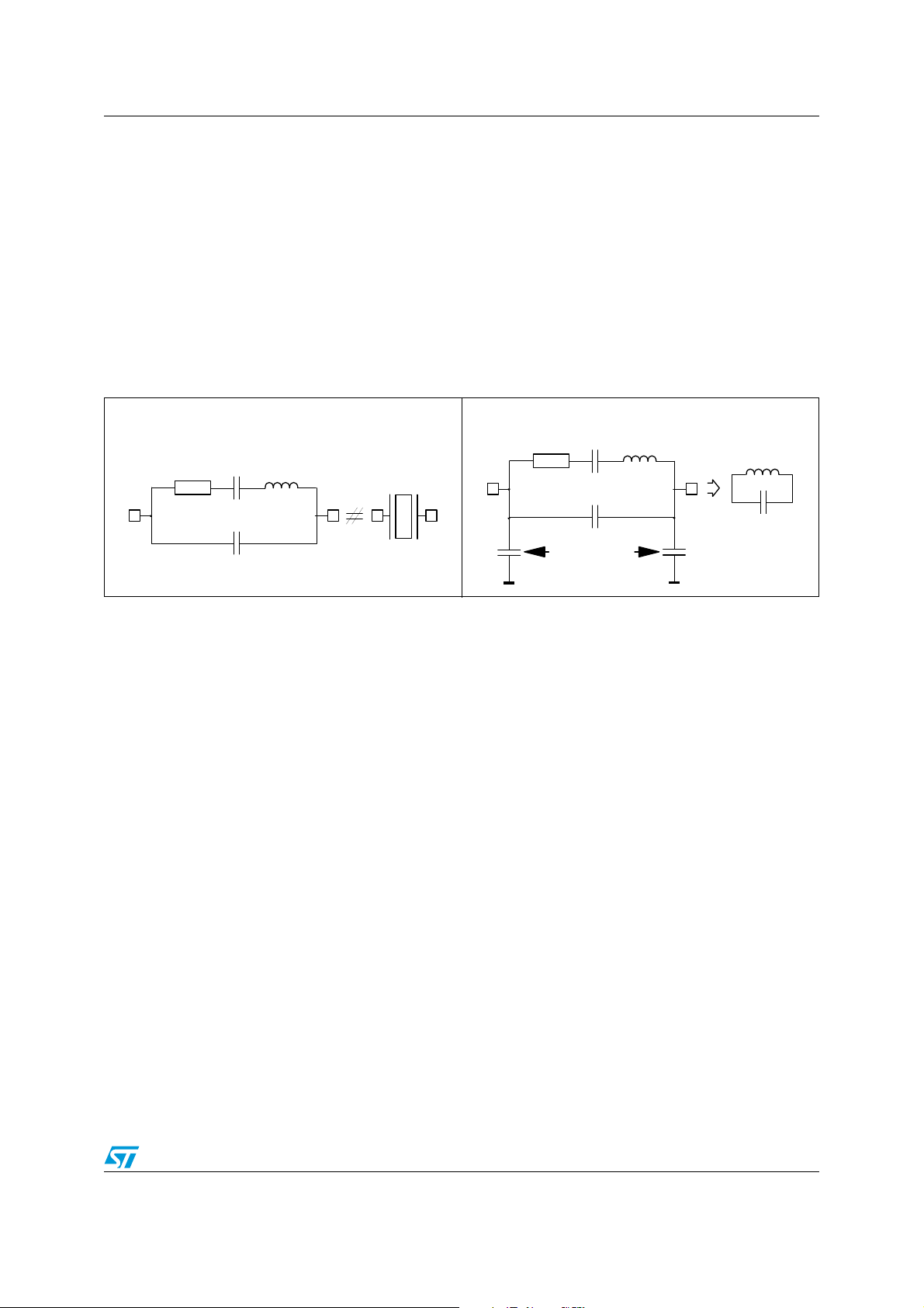
AN670 Oscillation frequency
C
1
L
R
Co
C
1
L
C
ext
R
Co
1 Oscillation frequency
The resonator can be modelised by a serial/parallel oscillator circuit as described in
Figure 1.
Figure 1.
The additional capacitances C
define a stable oscillating frequency. The value of these capacitances is usually given by the
manufacturer of the resonator.
The oscillation frequency is the resonant frequency of the equivalent circuit given in
Figure 2. The resonator is inductive in the oscillation frequency range.
are usually connected to the oscillator pins in order to
ext
Resonator model Figure 2. Equivalent circuit
3/12
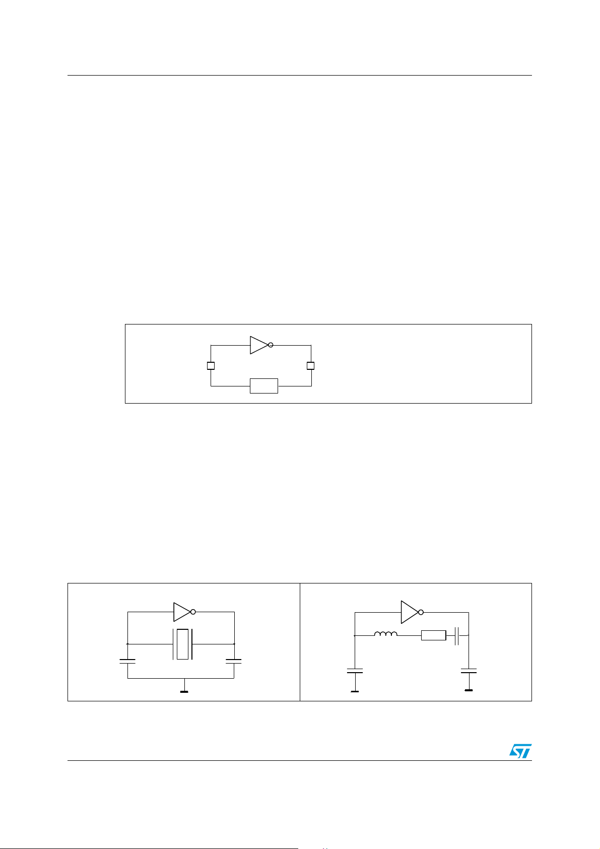
Oscillation conditions AN670
G
B
Input
Output
G: Inverter/Amplifier
B: Resonator circuit
Vout
Vin
Cout
Cin
Cout
Cin
+
-
+
LR
Co
2 Oscillation conditions
The proposed method is based on the Barkhausen criteria. This leads to a safe result
providing that the oscillator fulfills these criteria. Three points have to be analysed: oscillator
start-up, frequency stability and the start-up time.
2.1 Barkhausen criteria
An oscillator can be modelized as defined in Figure 3. B is the resonator gain and G the
amplifier/inverter gain. The value of BxG defines the oscillator behaviour:
● BxG >> 1: square waveform, start-up OK
● BxG > 1: waveform with harmonic distortion, start-up OK
● BxG = 1: sine waveform, start-up critical
● BxG < 1: no oscillation
Figure 3. Oscillator model
2.2 Start-up
The oscillator can start if the gain BxG is above 1. The amplifier gain must compensate for
the resonator circuit attenuation and provide a sufficent gain margin (>3 dB).
In addition, the resonator circuit B must introduce a 180 ° phase delay if the G amplifier is an
inverter and no rotation if it is a non inverting amplifier.
With classical circuits such as a Pierce type oscillator (Figure 4.), the 180 ° phase rotation is
due to capacitances (C
Figure 4. Pierce type oscillator Figure 5. Equivalent schematic at the
and Cin).
out
resonant frequency
4/12

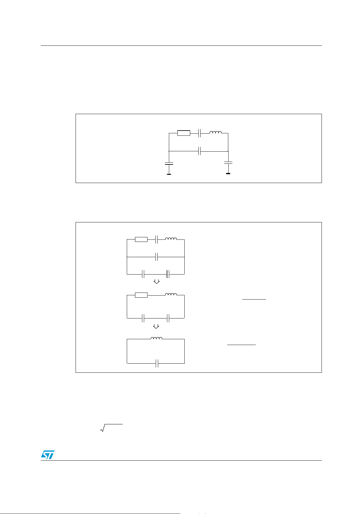
AN670 Oscillation conditions
S
OSCin
OSCout
V
1
V
2
Cin Cout
C
probe
At the resonance frequency (serial mode), the circuit can be modelized as described in
Figure 5. The resonator voltage is balanced between the two capacitances. So the phase of
the voltages V
either higher (C
The trade offs in the choice of C
● C
out
and V
in
out>Cin
= Cin : Vin = V
is delayed by 180 °. Depending on the capacitance values, Vin is
out
), smaller (C
in
out
out<Cin
and C
) or equal to V
are:
out
out
.
This is the typical case and is to be used as often as possible.
● C
> Cin : Vin > V
out
out
The loop gain is increased but there is a risk that the oscillation occurs at a harmonic of
the resonator frequency.
● C
< Cin : Vin < V
out
out
The output voltage is increased. The risk of oscillation at a harmonic of the resonator
frequency is low. V
must be high enough to satisfy the condition BxG >1.
in
2.3 Measurement of the loop gain (open loop)
The measurement is based on the schematic shown in Figure 6. The method is the
following:
1. Open the loop as described in Figure 6.
2. Place an oscillator probe on points 1 and 2. Note that the real C value for the
calculation is C
3. Inject a voltage S with a signal generator. This signal must be adjusted in frequency to
maximize the voltage V
4. Adjust S to a value small enough to avoid saturation of the amplifier (around 200 mV on
V
).
1
5. Calculate the ratio V
If the ratio is above +3 dB, the oscillator start is safe. If it is below, C
probe
+ Cin.
.
2
. This value has to be between +3 and +10 dB (1.5 to 3).
1t/V2
should be decreased.
in
Figure 6.
Gain loop measurement schematic
2.4 Frequency stability
The stability is first defined by the resonator characteristics. Nevertheless, if the open loop
gain exceeds +10 dB, the oscillation could occur on a harmonic of the resonator frequency.
In such cases, the value of C
rejecting this harmonic must be added.
should be increased to reduce the loop gain or a filter
in
5/12

Oscillation conditions AN670
Cin
2
Cin
2
Vcc
Cout
2.5 Start-up time
The start-up time depends on the amplifier polarisation time and on the circuit transients.
The polarisation of the amplifier can be accelerated by dividing the C
described in Figure 7.
capacitance in two as
in
Figure 7.
The start-up time is also longer when Cin and C
start-up time (i.e. low frequency quartz crystal), these capacitances values should be as
small as possible. Generally, the higher the crystal Q factor and lower the crystal frequency,
the longer the start-up time.
Amplifier polarisation acceleration
are increased. As a result, for very low
out
6/12

AN670 Conclusion
3 Conclusion
This note describes a method to choose oscillator network capacitances adapted to
standard resonators and quartz crystals (i.e. rs < 60 ohms and gain > 500). Since several
network values can be chosen, the capacitances values should be minimized in order not to
affect the resonance frequency and reduce the start-up time.
7/12

Test of a CSA Murata crystal resonator with an ST6210xx AN670
Appendix A Test of a CSA Murata crystal resonator with
an ST6210xx
A.1 Choice of the network capacitances
Resonator equivalent values:
L = 385 µH
C
= 4.4 pF
0
C
= 36.3 pF
1
rs = 8.7 ohm
Q = 1134
The oscillation mode is the fundamental mode.
The recommended load capacitances for 4 MHz oscillation frequency are 2x30 pF.
The corresponding oscillation frequency as calculated from the formula given in Appendix B
is 4.03 MHz.
A.2 Pseudo closed loop measurement
In the worst case (T
+13.6 dB.
ambiant
max, V
min) the gain V
supply
A.3 Start-up time
The start-up time is measured in closed loop. In the worst conditions (T
min), it is less than 1 ms.
A.4 Conclusion
The selected ceramic resonator matches with the ST6210 oscillator.
is 4.8. So the safety margin is
out/Vin
max, V
ambiant
supply
8/12
AN670 Calculation of the resonant frequency of ceramic resonator
R
Co
L
C1
C2 C3
RL
Co
RL
C
1
C2
C3
Co
Ceq
C'
L
Where C
' =
C
o +
Ceq
C
o x Ceq
Where Ceq = C
1 +
C
2 + C3
C2 x C3
f
1
2π LxC′
--------------------------=
Appendix B Calculation of the resonant frequency of
ceramic resonator
B.1 Equivalent circuit at the resonance frequency
Figure 8. Equivalent circuit
B.2 Transformation for simple calculation
B.3 Resonant frequency
Figure 9. Transformed circuit
9/12

Calculation of the resonant frequency of ceramic resonator AN670
B.4 Note
When using a ceramic resonator, the oscillation frequency is usually between the parallel
and the series resonances. So both C
The resonance frequency of a crystal resonator is very near to the serial frequency. So only
Co has to be used for the frequency calculation.
and Co have ot be included in the calculation.
1
10/12

AN670 Revision history
4 Revision history
Table 1. Document revision history
Date Revision Changes
February-1994 1 Initial release.
Format changed.
03-Oct-2008 2
Title of Appendix A modified (ST6210xx instead of ST6210).
Logo and disclaimer updated.
11/12

AN670
Please Read Carefully:
Information in this document is provided solely in connection with ST products. STMicroelectronics NV and its subsidiaries (“ST”) reserve the
right to make changes, corrections, modifications or improvements, to this document, and the products and services described herein at any
time, without notice.
All ST products are sold pursuant to ST’s terms and conditions of sale.
Purchasers are solely responsible for the choice, selection and use of the ST products and services described herein, and ST assumes no
liability whatsoever relating to the choice, selection or use of the ST products and services described herein.
No license, express or implied, by estoppel or otherwise, to any intellectual property rights is granted under this document. If any part of this
document refers to any third party products or services it shall not be deemed a license grant by ST for the use of such third party products
or services, or any intellectual property contained therein or considered as a warranty covering the use in any manner whatsoever of such
third party products or services or any intellectual property contained therein.
UNLESS OTHERWISE SET FORTH IN ST’S TERMS AND CONDITIONS OF SALE ST DISCLAIMS ANY EXPRESS OR IMPLIED
WARRANTY WITH RESPECT TO THE USE AND/OR SALE OF ST PRODUCTS INCLUDING WITHOUT LIMITATION IMPLIED
WARRANTIES OF MERCHANTABILITY, FITNESS FOR A PARTICULAR PURPOSE (AND THEIR EQUIVALENTS UNDER THE LAWS
OF ANY JURISDICTION), OR INFRINGEMENT OF ANY PATENT, COPYRIGHT OR OTHER INTELLECTUAL PROPERTY RIGHT.
UNLESS EXPRESSLY APPROVED IN WRITING BY AN AUTHORIZED ST REPRESENTATIVE, ST PRODUCTS ARE NOT
RECOMMENDED, AUTHORIZED OR WARRANTED FOR USE IN MILITARY, AIR CRAFT, SPACE, LIFE SAVING, OR LIFE SUSTAINING
APPLICATIONS, NOR IN PRODUCTS OR SYSTEMS WHERE FAILURE OR MALFUNCTION MAY RESULT IN PERSONAL INJURY,
DEATH, OR SEVERE PROPERTY OR ENVIRONMENTAL DAMAGE. ST PRODUCTS WHICH ARE NOT SPECIFIED AS "AUTOMOTIVE
GRADE" MAY ONLY BE USED IN AUTOMOTIVE APPLICATIONS AT USER’S OWN RISK.
Resale of ST products with provisions different from the statements and/or technical features set forth in this document shall immediately void
any warranty granted by ST for the ST product or service described herein and shall not create or extend in any manner whatsoever, any
liability of ST.
ST and the ST logo are trademarks or registered trademarks of ST in various countries.
Information in this document supersedes and replaces all information previously supplied.
The ST logo is a registered trademark of STMicroelectronics. All other names are the property of their respective owners.
© 2008 STMicroelectronics - All rights reserved
STMicroelectronics group of companies
Australia - Belgium - Brazil - Canada - China - Czech Republic - Finland - France - Germany - Hong Kong - India - Israel - Italy - Japan -
Malaysia - Malta - Morocco - Singapore - Spain - Sweden - Switzerland - United Kingdom - United States of America
www.st.com
12/12
 Loading...