

Page 1

AN668
APPLICATION NOTE
A New High Power IC Surface Mount Package Family: PowerSO-20
& PowerSO-36 Power IC Packaging from Insertion to Surface Mount
by P. Casati & C. Cognetti
A new, high power IC surface mount package family is
introduced in this note. It is called Power SO famil y and
has the Jedec registration MO-166.
STMicroelectronics developed PowerSO in order to
answer the increasing demand of miniaturization and
quality in power applications. Automotive, industrial,
audio and telecom markets will take advantage of the
new package, by introducing the use of S urface Mount
Technology in the production of power systems.
PowerSO-20 and PowerSO-36 are the elements of the
MO-166 family having 20 leads at 0.050 inch pitch
(1.27 mm) and 36 leads at 0.026 inch pitch (0.65 mm)
respectively. These packages are in mass production
since 1995.
PowerSO-20 – Jedec Registration MO-166
™
ing
This note is intended to compare the PowerSO-20/36 with alternative surface mount solutions and to
the existing Multiwatt package, the well known "double TO-220" developed by STMicroelectronics in
late 70s.
Data presented here demonstrates that PowerSO-20 is the real successor of Multiwatt for surface mount
applications and is becoming a milestone in power package technology with PowerSO-36 as Multiwatt
did 20 years ago.
1. POWER DEVICES AND SURFACE MOUNTING
Use of Surface Mount Technology (SMT) has dramatical ly increased in the last 20 years, moving from consumer
to professional applications and serving highly demanding markets like telecom, industrial and automotive.
Major advantages expected from SMT are size reduction, automated board mounting, high reliability and cost
effectiveness; larger density of functions is achieved in smaller systems.
Evolution of SMT drove the development of several new packages for discrete and IC devices: SOT23,
SOT194, TO263, SO, PLCC, PQFP with many options in pin pitch, size and thickness.
All of them are compatible with the surface mount technique, based on fast picking and placing from tapes or
trays, followed by mass soldering. Mounting lines are almost totally automated, with high throughput and high
yield.
Only a few devices are not y et compati ble w ith SMT princi ples: a few "exotic" components like l arge capac itors,
resistors, inductors, varistors, etc. and almost all the power semiconductor packages. Several drawbacks are
associated with existing power packages:
July 2001
1/19
Page 2

AN668 APPLICATION NO TE
1) They have still the traditional structure for insertion and are mounted manually in the PCB,
with loss of time, productivity, floor space and
money;
2) They force the use of wave soldering techniques and are not compatible with reflow soldering;
3) They are not compatible with increasing need
of miniaturization of power systems.
The above points are so important that the development of totally new power packages fitting the SMT
requirements is a clear demand of the industry and
can pay back the heavy effort needed in terms of
R&D, engineering and production resources.
1.1 INTERMEDIATE SOLUTIONS: INSERTION
PACKAGES CONVERTED TO SMT
The fastest answer to the requirement discussed
above is the adaptation of existing insertion packages to obtain a kind of surface mount configuration.
This can be conveniently done by redesigning the
lead shape, as in the case of the surface mount Heptawatt package (7 lead TO-220) shown in Figure 1
which was introduced in the market by STMicroelectronics in 1989.
The package of Figure 1 is very attractive in terms of
capital expenditure and time to market; as a minor
modification of existing production line can provide
the surface mount version in a short development
time.
However, the experience of STMicroelectronics with
above solutions is not totally satisfactory, for a number of reasons:
Figure 1.
HeptawattTM (surface mount) package
ture, which is asymmetrical in two directions
(height and thickness). Existing pick and place
tools are not readily compatible with this structure, as well as the tape and reel packing;
2) SIZE, which is basically the same as existing
insertion packages; therefore, is not the answer to the demand of miniaturization of power
systems coming from almost all the applications: automotive, audio and industrial;
3) COPLANARITY, which can become an issue
for 4-6 mm (0.16-0.24 inch) long leads. It must
be recalled tha t maj or c oplanar ity im provement
is obtained by reducing the lead length, down
to 1-2 mm (0.04-0.08 inch); this cannot be
readily obtained with Multiwatt, whose average
leadframe thickness is about 0.4 mm.
4) RELIABILITY AFTER THE SOLDERING PROCESS, due to the excess stress caused by the
high temperature (>215°C) even with "zero"
absorbed moisture at the large interface between slug and molded body, with consequent
delamination;
5) INSPECTION OF THE SOLDERED JOINT between slug and substrate, as discussed in next
paragraph;
6) LIMITED PIN COUNT 7, which is no longer
able to cover the requirements of advanced
smart power, needing more I/Os for the logic
circuitry.
Due to the above reasons, STMicroelectronics preferred to invest in new especially developed power
structures, with designed-in surface mount characteristics. Moreover, due to the increasing demand of
quality, led by the automotive market, process and
materials were selected in order to obtain intrinsic
long term reliability and a very low failure rate, targeted at 1 ppm for early life.
1) HANDLING, which unlike all other surface
mount packages, is complicated by the struc-
2/19
1.2 NEW SOLUTI ONS:
ORIGINAL STMicroelectronics P ACKAGES
WITH D ESIGN-IN SMT CHAR ACTERISTIC S
The well understood dual-in-line configuration was
selected for the new housing (Figure 3), which does
not look very much different than the Small Outline
(SO) package; but, from high dissipation capability,
the main difference is the internal massive slug,
which provides the same thermal impedance as traditional insertion packages.In view of the larger pin
count needed for smart power products, a family of
Page 3
AN668 APPLICATION NOTE
packages has been designed, cov eri ng from 2 0 to 36
leads. The well established concept of "variable pitch
in a fixed body" has been used, with 1.27 mm (0.05
inch), 1.0 mm, 0.8 mm and 0.65 mm.
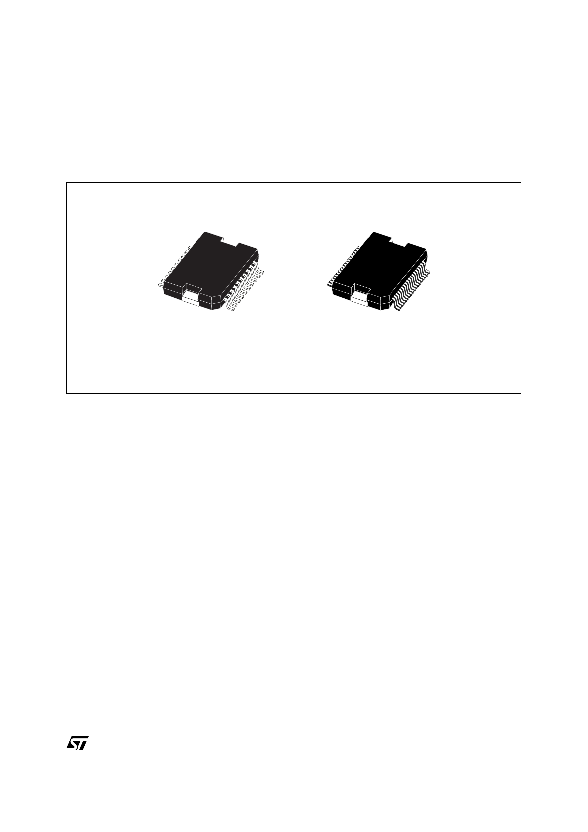
Figure 2.
PowerSO-20 & PowerSO-36 packages
PowerSO-20
The new family, named PowerSO, is Jedec registered as MO-166.
PowerSO-20 and PowerSO-36 are presented in this
technical note (Figure 3 & 4)
PowerSO-36
3/19
Page 4
AN668 APPLICATION NO TE
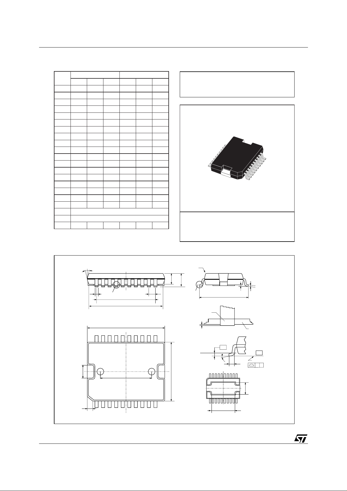
Figure 3. PowerSO-20 package (Jedec MO-166) mechanical data.
DIM.
mm inch
MIN. TYP. MAX. MIN. TYP. MAX.
A 3.6 0.142
a1 0.1 0.3 0.004 0.012
a2 3.3 0.130
a3 0 0.1 0.000 0.004
b 0.4 0.53 0.016 0.021
c 0.23 0.32 0 .009 0.013
D (1) 15.8 16 0.622 0.630
D1 9.4 9.8 0.370 0.386
E 13.9 14.5 0.547 0.570
e 1.27 0.050
e3 11.43 0.450
E1 (1) 10.9 11.1 0.429 0.437
E2 2.9 0.114
E3 5.8 6.2 0.228 0.244
G 0 0.1 0.000 0.004
H 15.5 15.9 0.610 0.626
h 1.1 0.043
L 0.8 1.1 0.031 0.043
N 10˚ (max.)
S
8˚ (max.)
T10 0.394
(1) "D and F" do not include mold flash or protrusions.
- Mold flash or protrusions shall not exceed 0.15 mm (0.006").
- Critical dimensions: "E", "G" and "a3"
OUTLINE AND
MECHANICAL DATA
JEDEC MO-166
PowerSO20
E2
h x 45
DETAIL B
PSO20MEC
R
lead
a3
Gage Plane
BOTTOM VIEW
E
DETAIL B
0.35
S
D1
L
c
a1
DETAIL A
slug
- C -
SEATING PLANE
GC
(COPLANARITY)
E3
NN
a2
A
b
DETAIL A
e3
H
D
T
1
e
1120
E1
10
4/19
Page 5

Figure 4. PowerSO-36 package (Jedec MO-166) mechanical data.
AN668 APPLICATION NOTE
DIM.
mm inch
MIN. TYP. MAX. MIN. TYP. MAX.
A 3.60 0.141
a1 0.10 0.30 0.004 0.012
a2 3.30 0.130
a3 0 0.10 0 0 .004
b 0.22 0.38 0.008 0.015
c 0.23 0.32 0.009 0.012
D (1) 15.80 16.00 0.622 0.630
D1 9.40 9.80 0.370 0.385
E 13.90 14.50 0.547 0.570
e 0.65 0.0256
e3 11.05 0.435
E1 (1) 10.90 11.10 0.429 0.437
E2 2.90 0.114
E3 5.80 6.20 0.228 0.244
E4 2.90 3.20 0.114 0.126
G 0 0.10 0 0.004
H 15.50 15.90 0.610 0.626
h 1.10 0.043
L 0.80 1.10 0.031 0.043
N10°(max.)
S8°(max.)
(1): "D" and "E1" do not include mold flash or protrusions
- Mold flash or protrusions shall not exceed 0.15mm (0.006 inch)
- Critical dimensions are "a3", "E" and "G".
OUTLINE AND
MECHANICAL DATA
PowerSO36
NN
a2
A
1936
0.12 AB
⊕
e
M
E1
DETAIL B
lead
a3
B
Gage Plane
PSO36MEC
BOTTOM VIEW
DETAIL B
0.35
S
L
E
DETAIL A
(COPLANARITY)
E2
h x 45˚
DETAIL A
118
A
e3
H
D
b
c
a1
slug
E3
D1
- C -
SEATING PLANE
GC
5/19
Page 6
AN668 APPLICATION NO TE
The most important features of PowerSO-20/36 are:
1) High power structure and process;
2) High current capability;
3) Miniaturization
4) Designed-in surface mount characteristics:
a] Handling;
b] Tape and reel packing;
c] Co-planarity;
d] Solder joint quality and inspection;
e] High reliability after soldering process.
5) Designed-in "hermeticity", for low failure rate (1
ppm).
2. STRUCTURE AND CHARACTERISTICS
OF POWERSO-20/36
.
In this section, design criteria listed in previous paragraph are presented and discussed.
2.1 High power structure and process (>20 W)
The main feature of the power package structure is
the existence of a massive copper slug in the package onto which the silicon chip is soldered. Its function is twofold:
a) To provide a low thermal resistance path from
the chip to the external heatsink;
b) To provide a large thermal capacitance, able to
absorb power peaks in switching conditions.
The slug of PowerSO-20/36, is optimized in order to
get a good compromise between miniaturization and
thermal performance. As a result of this work, PowerSO-20 has the same junction to case thermal resistance Rth(j-c) of Multiwatt package and the same
thermal impedance up to 0.5 sec. Therefore the
range of application exceeds 20 W, the same as for
traditional power packages.
Section 3 will present thermal design in detail. Here
we will recall the importance of the die attach process, typical of power IC packages, which uses a
high melting temperature (300°C) tin based alloy.
The control of this process, in terms of solder thickness and void reduction, is based on SPC methods
and has a CPK > 1.33.
2.2 High current capability (10-20 A)
At first glance, leads of the PowerSO-20/36 seem
very fragile, thin and not compatibl e with the high c ur-
rents (10-20 A) associated with a large number of
power ICs, which require the utilization of large aluminum wires having a diameter ranging between
0.010 and 0.020 inch (0.25 to 0.5 mm).
Table 1 reports the comparison of PowerSO-20 with
insertion and surfac e mount Mul tiwatt and the following considerations are possible:
1) Electrical resistance of PowerSO-20 leads is
about 760
µΩ
, i.e. it is equivalent to insertion
Multiwatt or better;
2) Electrical resistance of PowerSO-20 leads is
worse than Surface Mount Multiwatt by a factor
of 1.3 to 2;
3) In any case, lead resistance of PowerSO-20 is
much lower than the wire resista nce. Wire resistance is 450-1800
µΩ
/mm and it must be
considered that the minimum wire length is 2.5
mm corresponding to 1150-4500
µΩ
;
4) If needed, two or more leads are short circuited
and different frame designs can be developed
providing flexible options (Figure 6). With multiple wire bonding, current capability can be
very large; for 45A current, if 3 leads are used
with 10 mil diameter, 3 mm long wires, electrical resistance of the interconnection is about
Ω
2m
.
Table 1.
Electrical resistance data of PowerSO-20
and Multiwatt 15 leads
Dimensions
(mm)
Long lead
MW15
23x0.9x0.5
18x0.9x0.5
Short lead
MW15
14x0.9x0.5
9x0.9x0.5
Lead
PowerSO-20
5x0.5x0.25 – – 760µΩ
Multiwatt15
Insertion
970µΩ
–
590µΩ
–
Multiwatt15
Surf. Mount
–
760µΩ
–
380µΩ
PowerSO-20
–
–
–
–
Copper resistivity : 1.9mW x cm
Aluminum wire resistance:
∅
10 mils: 1800 mW / mm
∅
20 mils: 450 mW / mm
6/19
Page 7

AN668 APPLICATION NOTE
2.3 Miniaturization
The whole story of microelectronics has been a continuous race towards smaller products. This is also
true for power systems.
The PowerSO-20 and PowerSO-36 offer excellent
possibilities in miniaturization, without compromising
power dissipation.
From Table 2, which compares the PowerSO-20 with
the surface mount version of Multiwatt, advantages in
terms of size, weight, height and vol ume ar e evident.
They range between 22 and 64% improvement.
Table 2. Miniaturization of PowerSO-20 vs Sur-
face Mount Multiwatt
footprint
2
(mm
height
(mm)
volume
3
(mm
SM MW15L
320 227 -30%
)
4.5 3.5 -22%
1160 590 -49%
)
PowerSO-20
Difference
2.4 Designed-in surface mount characteristics
A] Handling
The PowerSO-20/36 structure is similar to the
SO outline, which was introduced more than 20
years ago in STMicroelecrtronic s. Ther efore, the
experience associated with the different aspects
of production, testing, burn-in and on board
mounting are quite solid.
Due to their optimized outline and reduced
weight, handling of the PowerSO-20/36 packages does not present any particular problem and
is fully compatible with existing equipment.
B] Packing
Tube and Tape & Reel packing are both possi ble
with the PowerSO-20/36. Embossed cavity tape
has been produced with a special design, able to
minimize the mechanical effect of packing and
shipment on the lead coplanarity (Figure 6).
weight (gr) 5.6 1.9 -64%
Figure 5. Frame options for high current
D94IN001
7/19
Page 8

AN668 APPLICATION NO TE
Figure 6. Embossed cavity tape.
1.5 +0.1/-0.0
8.6013.00Bo
4.50
11.50
Ao
30 ±0.05
STRETCH
FORM
C] Coplanarity
Lead coplanarity is considered a major issue for
surface mount devices. In the case of Power surface mount packages, whose slug is eventually
soldered on a substrate, coplanarity is also referenced to the relative position of the slug and the
leads.
In the PowerSO-20/36, lead extremities and
package slug are positioned inside a 4 mil (0.1
mm) layer; this condition provides a high yield
mounting and soldering process.
D] Solder joint quality and inspection
When the package slug is soldered onto the sub-
strate, as in the many applications developed so
far, the need exists for producing a high quality
solder joint between the slug and its solder pad on
the board.
The PowerSO-20/36 structure is ideal from this
viewpoint: symmet ry exis ting in the x- y plane provides a very good balance of the wetting forces,
once the solder paste is melted. A kind of self
centering effect has been observed, which is
mostly due to the dual-in-line outline and to the
excellent wettability of both leads and slug. This
2.00
4.00
24.00
Ko
1.00
A
A
1.75
11.50
24.00 ±0.3
R0.50 Typical
1.50 min
D94AN002
results in a solder joint well contr olled in thicknes s
and consistency.
An additional advantage of the PowerSO-20/36
outline is the presence of two exposed inspection
points on the slug, which has been intentionally
obtained in the package body (Figure 7). Proprietary processes keeps these two points free of
molding compound flash and allows evident solder fillets after the soldering process.
Due to the symmetrical structure of PowerSO20,/36 the presence of solder fillet in both inspection points is a good indicator of joint quality and
planarity. It should be noticed that the same kind
of control is not possible in the surface mount
Multiwatt structure, which can show a good solder
fillet in the exposed section of the slug even with
a non-parallel joint and possible voiding. In this
case, the degradation of the junction to substrate
thermal resistance Rth(j-s) is more evident, as
shown in Figure 8.
E] Reliability after soldering process
Extensive evaluation of frame design and materi-
als provides the PowerSO-20/36 excellent reliability performance after the soldering process,
as discussed in section 5. No degradation of the
8/19
Page 9
AN668 APPLICATION NOTE
A
package structure has been observed after the
high temperature stress, up to 260°C.
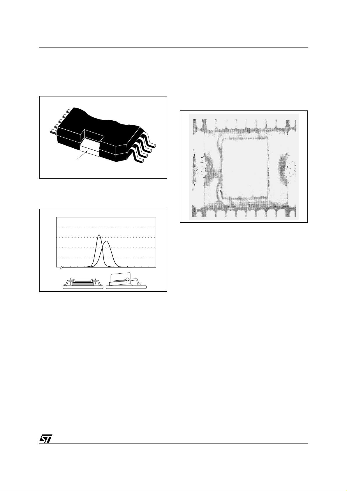
Figure 7. Exposed slug edge for solder joint in-
spection
slug edge accessible
for visual inspection
D94AN003
Figure 8. Loss of thermal performance due to
poor co-planarity and uneven solder
joints
100
%
80
60
40
20
0
Power SO-20/36
MW SMT
VERSION
D94AN004
R
th(j-s)
quence, Scanning Acoustic Microscopy (SAM)
analysis and die penetration test confirms the robustness of the PowerSO-20/36. Figure 9 shows a typical
map of adhesion obtained in SAM evaluation after
stress analysis.
Figure 9. Scanning Acoustic Microsco pe m ap
3. THERMAL DESIGN AND APPLICATIONS
Thermal characteristics of the new PowerSO-20/36
package can cover a wide r ange of applications , both
in the medium power (1-5W) and in the high power
range (up to 20W). Moreover, as sufficiently large
thermal capacitance is associated with the new package, performance in switching conditions is equivalent to that of available insertion packages.
2.5 Hermeticity
Good hermeticity of package interfaces has been obtained by means of slug design and of the selection
of low stress, high adhesion molding compounds.
State-of-the-art molding equipment and process is
used, with CPK in excess of 1.33 for all the key parameters. This provides repeatability of the results in
large volumes.
Moreover, improved mechanical clamping of the
molding compound is obtained by using a new, proprietary finishing of the slug all along its periphery,
which is provided with undercutting and controlled
surface roughness.
After severe tests consisting of alternate thermal cycling and pressure pot, and after the "pop corn" se-
In this section, a number of typi cal applicati ons of the
PowerSO-20/36 will be considered and compared
with existing solutions, taki ng into acc ount that a major role in the thermal design is played by the temperature increase Tj-Ta specified in the different
applications. "Delta" Tj can be as low as 25-30°C in
extreme conditions for automotive or as large as
100°C in more relaxed systems.
Unless differently indicated,
∆
Tj of 50°C is assumed
in all the considerations of this note.
3.1 JUNCTION-TO-CASE THERMAL RESISTANCE
The main feature of PowerSO-20/36 packages are
optimization of junction-to-case thermal resistance,
from the junction to the external surface of the slug.
Unlike standard SO packages, which use epoxy die
9/19
Page 10

AN668 APPLICATION NO TE
attach and thin leadframes, the PowerSO-20/36 take
advantage of power package technology, with a massive copper slug and tin based alloy die soldering.
This results in minimum junction-to-case thermal resistance Rth(j-c). Figur e 10 shows how muc h Rth(j-c)
is affected by the die size, assuming that the power
source is uniformly distributed on the die.
For actual applications , Rth(j-c) ranges between 2°C/
W for small dice and 0.5°C/W for the maximum die
size of 60k sq mils. Therefore, the PowerSO-20/36
are equivalent to inserti on power packages li ke TO-220
and Multiwatt; this is due to the optimization of the
slug dimensions, obtained by removal of any copper
in excess, without affecting the thermal cone where
the heat flows from the silicon to the substrate.
The PowerSO-20/36 offer a new possibility for a power package: direct soldering of the slug onto the
board during the surface mount process; therefore
junction to substrate thermal resistance is close to
Rth(j-c) and reaches the very attractive value of 0.5-
2.0°C/W.
Figure 10. Thermal resistance junction-case
vs. dissipating area of PowerSO-20/36
with a modified leadframe in order to have a number
of leads connected to the die pad (bat wing structure).
This solution, shown in Figure 11, is effective in minimizing the Junction-to-Pin thermal resistance Rth(jp), i.e. the thermal path between the junction and
suitable dissipating areas obtained on the PCB and
connected to the heat transfer leads (Figure 12).
Figure 11. Lead frame for medium power SO
Figure 12. Foot print for medium power SO
R
th
2.5
2.3
2.1
1.9
1.7
1.5
1.3
1.1
0.9
0.7
0.5
012345
die thickness: 0.375mm
Pd=5W
on die dissipating area
silicon
side L(mm)
D94AN005
side L
3.2 APPLICATIONS WITH 1-2 WATT DISSIPATION
3.2.1 On board dissipating elements
In this power range, state of the art technology is
based on the medium power SO.
It has the same outline of a standard SO package but
D94AN006
Typical representatives of the medium power SO
package family are the 300 mils SO20 and SO28 with
8 heat transfer leads, reported as SO(12+4+4) and
SO(20+4+4) respectively.
Referring to STMicroelectronics guideline "Thermal
management in Surface Mount Technology" (July
1988), thermal performance of medium power
SO(12+4+4) is defined by the relationship:
Rth(j-a) = Rth(j-p) + Rth(sub-amb)
where Rth(j-p) is the ther mal path from the juncti on to
the board and Rth(sub-amb) is the thermal resistance of the two areas shown in Figure 12.
Rth(j-p) ranges between 12 and 14°C/W, depending
10/19
Page 11

AN668 APPLICATION NOTE
on the efficiency of the heat transfer leads (design
and thermal conductivity) and on the die size.
Rth(j-a) is due to the size of the dissipating elements
on the board, according to Figure 13, which shows
improved thermal resistance from 76 to 50°C/W
when the dissipating area is incr eased from 0 to 6 cm
sq.
The PowerSO-20/36 can be used in place of medium
power SO, with the slug soldered on the board.
Figure 13. Rth(j-a) vs. board dissipating area
R
(˚C/W)
th(j-a)
80
75
70
65
60
55
50
45
012345678910
on board heat sink area (sq.cm)
die pad = 140 x 220sq.mils
die size = 120 x 130sq.mils
Pd = 1W
D94AN007
The first experimental evidence shows a very good
heat exchange with the substrate, due to the large
contact area associated with the basic footprint of
Figure 14. Rth(j-a) is about 50°C/W in this configuration.
Figure 14. Pad layout
17.7
14.8
When the two dissipating elements are added and
the footprint of Figure 15 is used, additional improvement is observed. For example, Rth(j-a) is 35°C/W
with dissipation elements of 6 sq cm.
Figure 15. Footprint with dissipating elemen t
D94AN009
Margin over the traditional medium power
SO(12+4+4) is about 40%, w ith dissipati on increased
from 1 W to 1,4 W always with Delta Tj = 50°C. Improvement can be also understood taking into account that the junction to substrate thermal
resistance is equivalent to Rth(j-p) = 12-14°C/W for
medium power SO(12+4+4) and equivalent to Rth(jc) = 0.5-2.0°C/W for PowerSO-20/36.
3.3 APPLICATIONS WITH 2-5 WATT DISSIPATION
3.3.1 Dissipating elements and ground layer
It must be noticed that previous data are observed
with a simple PCB, with single or double face. In applications using mult ilayer boards , a much better efficiency is observed due to the heat spreading effect of
the ground layer.
Looking at the board s tructure of Fi gure 16, heat generated at the junction is transferred to the dissipating
areas on the board surface and then to the ground
layer, which works as a large heat exchan ge element
with the ambient.
Rth(j-a) offered by this solution is 20-25°C/W for 2.0
- 2.5W dissipation.
5
1.7
0.7 1.27
9.4 15.4
D94AN008
Figure 16. M ounting on PCB wi th gro und laye r
Ground
layer
D94AN010
11/19
Page 12

AN668 APPLICATION NO TE
3.3.2 Via holes and ground layer
If via holes are used as in Figure 17, a more direct
thermal path is obtained from the slug to the ground
layer. The number of vias is chosen according to the
desired performance.
Figure 18 shows a typical high performance foot print
for PowerSO20/36 with via holes
Rth(j-a) can be reduced down to 15-20°C/W and dissipation increased up to 2.5-3.3W with Delta Tj =
50°C.
Figure 17. Mounting on epoxy FR4 using via
holes for heat transfer of ground layer
Copper
foil
Ground
layer
via holes
D94AN011
Figure 18. Footprint of PowerSO20/36 with via
holes
3.3.3 Via holes and external heatsink
The solution considered in Figure 19 combines a PowerSO-20/36 soldered onto a via hole structure, with a
metal plate glue d on the opposite side of the boar d.
The final thermal resistance value is given by the resistance of via holes added to the resistance of the
plate to the ambient.
Figure 20 shows the thermal resistance associated
with 16 holes and reports its behavior with the dissipated power. Hole depth of 1.5 mm is an extreme
case, existing in rather thick substrates only; the experimental value is about 9°/W, including the contribution of Rth(j-c). In practical cases, structures with
Rth(j-a) = 12-15°C/W are obtained for 3.3-4.2W dissipation.
Figure 19. Mounting on epoxy FR4 using via
holes for heat transfer and external
metal plate
Copper
foil
FR4 board
Metal plate
Via holes
D94AN012
Figure 20. Thermal Resistance junction-su b-
strate
R
(˚C/W)
thj-s
9.4
Mounted on FR4
9.2
Infinite heatsink
9.0
8.8
8.6
8.4
012345678910
Dissipated Power (W)
substrate with
Thickness: 1.5mm
D94AN013
vias holes
12/19
Page 13

AN668 APPLICATION NOTE
3.4 HIGH POWER APPLICATIONS (UP TO 20
W)WITH STANDARD SUBSTRATE
In order to get an Rth(j-a) of few °C/W, high power
applications requir e large and massiv e external he atsinks in close contact with the power device.
This is not a simple requirement when cost effective
systems using the standard surface mount technology and the standard PCB substrate are considered.
Major concerns are related to the critical assem bly of
a large heatsink onto a s mall package; vi brations and
thermal excursions c an gener ate unwanted mechanical stress, thus damaging the package leads or the
integrity of the contact between slug and heatsink.
However, the fact that we have a well established,
PCB based surface mount technology is pushing the
industry to test several directions, similar to those
sketched in Figure 21.
Rather than proven soluti ons, they should b e consi dered here as early attempts aimed to explore the capability of existing surface mount processes and
materials in the direction of increased heat dissipation at reduced cost.
3.4.1 "Slug-up" package and extern al heat-
sink
In the example of Figure 21a, PowerSO-20 is shown
in "reverse" or "slug-up" configuration, with a clip
mounted external heatsink, which was studied for
3.5W dissipation in still air and 5-6W dissipation in
forced ventilation.
Figure 21a. "Slug up"package with extern al
heatsink
Heatsink
Epoxy board
D94AN014
To minimize the mechanical stess on leads and solder joints derived from any pressure applied on top of
package, the slug-up formi ng is specifically designed
(Fig. 22).
3.4.2 Cavity board and extern al heatsink
In the example of Figure 21b, the PowerSO-20/36 is
mounted onto an epoxy board, with a through cavity
fabricated to correspond to the package slug. The external heatsink is directly applied in contact with the
slug, secured by means of a spring system or glued.
Also in this case, a high level of dissipation can be
achieved with properly designed heatsinks.
Figure 21b. Mounting on cavity board and ex-
ternal heatsink applied
Epoxy board
with through cavity
A similar concept can be used for other applications
and the sink size adapted to their specific requirements. A lar ge variety of solutions w ill exi st whic h will
take advantage of the metal box in which the board
can eventually be housed.
Heatsink
D94AN015
13/19
Page 14

AN668 APPLICATION NO TE
Figure 22. PowerSO-36 Slug-up
DIM.
A 3.25 3.5 0.128 0.1 38
A2 3.15 0.124
A4 0.8 1 0.031 0.0 39
A5 0.2 0.008
a1 0 0.1 0 0.004
b 0.22 0.38 0.008 0.015
c 0.23 0.32 0.009 0.012
D 15.8 16 0.622 0.630
D1 9.4 9.8 0.37 0.38
D2 1 0.039
E 13.9 14.5 0.547 0. 57
E1 10.9 11.1 0.429 0.437
E2 2.9 0.114
E3 5.8 6.2 0.228 0.244
E4 2.9 3.2 0.114 1.259
e 0.65 0 .026
e3 11.05 0.435
G 0 0.1 0 0.004
H 15.5 15.9 0.61 0.625
h 1.1
L 0.8 1.1 0.031 0.043
N 10˚ (max)
s 8˚ (max)
mm inch
MIN. TYP. MAX. MIN. TYP. MAX.
0.043
OUTLINE AND
MECHANICAL DA TA
PowerSO-36 (SLUG UP)
14/19
Page 15

AN668 APPLICATION NOTE
3.5 HIGH POWER APPLICATIONS (UP TO
20W) WITH INSUL A TE D ME TAL SUBSTRATES - IMS
In the last few years, several Companies developed
the idea of a cost effective Insulated Metal Substrate
(IMS) having:
a) A copper printed layer supported by an alumi-
num base, with epoxy or polyimide isolation in
between; or
b) A flexible printed circuit (polyimide) glued onto
an aluminum base.
In both cases, the following conditions are offered:
a) The substrate is compatible with s tandard SMT
processes, including infrared reflow soldering;
b) It is compatible with passive and active devic-
es, including PowerSO-20/36;
c) It has an acceptable thermal resistance loss
between the PowerSO-20/36 slug and the aluminum base, due to optimized thermal conductivity of the isolating layer;
d) The aluminum baseplate has variable thick-
ness, up to 5 mm, in order to sink different
amounts of heat.
Utilization of IMS is considered for several applications both for automotive and industrial systems and
is particularly fruitful when associated with PowerSO20/36 packages (Figure 23)
to the IMS by means of screws, bolts or rivets. The
total thermal resistance is obtained by adding the
heat sink resistance to the junction to baseplate resistance (1.0-2.5°C/W).
This solution is capable of 20-25 W per device and if
a large sink is used, as massive parts existing in the
car, more than one device can be assembled on the
same ISM, thus obtaining a functional power subsystem with several tens of Watt dissipation.
It is interesting to notice that the aluminum plate itself
has good dissipation properties to the ambient, depending on its size.
The PowerSO-20/36 soldered onto a 40 mm square,
1.5 mm thick IMS shows a thermal r esi stance of 7°C /
W, for about 7 W dissipation.
3.6 HIGH POWER PULSES AND THERMAL
IMPEDANCE
In several applications, large power pulses are delivered by the device for a short time.
In this case, discussed in the STMicroelect roni cs paper "Designing with Thermal Impedance" (Semitherm Conf. 1988), the quanti ty which rules the junc tion
temperature up to the time t0 is the thermal impedance of the three different elements: silicon chip,
package slug and heatsink.
Figure 23.
Copper
foil
Aluminium
Insulation
D94AN016
Thermal performance has been measured for both
substrates described above. The fir st result is related
to the contribution of isolation to the total thermal resistance. When the footprint of Figure 14 is used,
with the 96 sq mm slug soldered onto a 155 sq mm
pattern, this contribution is about 0.5°C/W .
Therefore, the thermal resis tance from the junction to
the aluminum baseplate ranges from 1.0 to 2.5°C/W
depending on the chip size.
For large dissipation, an external heat sin k is applied
For pulse durations in the range of 0.1-1.0 sec, the
package slug has the strongest influence on the system performance, depending on the associated thermal capacitance, i.e. the capability of heat
accumulation.
In the presence of properly sized slugs with suitable
capacitance, it is possible to maintain a low junction
temperature for the switching time of most applications, which seldom exceeds 1 sec.
For popular power packages like TO-220 and Multiwatt, the value of the thermal impedance in the first
second is lower than the value of Rth(j-c) in steady
state.
In order to compare the PowerSO-20/36 packages
with the insertion equivalent, Fig. 24 is very helpful. It
shows the thermal impedance of different packages
in the first second of the power pulse, in the same
conditions of power intensity and die size.
When similar comparisons are performed with medium power "bat wing" SO, the enhancement provided
15/19
Page 16

AN668 APPLICATION NO TE
by the copper sl ug becomes v ery evident ( Figure 2 5).
Due to the thermal capacitance of the slug, the tran-
sient thermal impedance of PowerSO-20/36 after 1
sec pulse duration is 4 times lower.
A summary of the thermal per formance of PowerSO20/36 considering the different mounting approaches
is given in Table 3, assum ing that the max imum rated
temperature of the device is 150°C and that the
∆
Tj
is 50°C.
Table 3. Thermal performance (∆Tj: 50°C)
PowerSO-20/36 packages
mounted on
1. FR4 using the reccomended pad lay-out
2. FR4 with heat sink on
board (6 cm2)
3. FR4 with heatsink (6
cm2) and ground
4. FR4 with 16 via holes
and ground layer
5. FR4 with 16 via holes
and external heatsink
6. IMS floating in air
7. IMS with external heat-
2
(40cm
)
sink applied
R
th(j-a)
50°C/W 1.0W
35°C/W 1.4 W
20°C/W 2.5W
15°C/W 3.3W
12°C/W 4.2W
7°C/W 7W
2.5°C/W 20W
Pdiss
Figure 24. Th erm a l impedance of di fferent
packages
Figure 25.
4. SOLDE R I NG INFORMAT IO N
The soldering process causes considerable thermal
stress to a s emiconduc tor com ponent. This has to be
minimized to ensure a reliable and extended lifetime
of the device.
PowerSO-20/36 are certified as MSL3 according to
Jedec STD 020A
As eflow techniques ar e the m ost c ommon in s urface
mounting, typical heating profiles are given in Figure
26, with a preheating at 130 - 150°C for 80 -100 seconds, either for mounting on FR4 epoxy substrate or
mounting on metal-backed boards (IMS). Peak temperature should be at least 30°C higher than the
melting point of the solder chosen.
Figure 26.
T (˚C)
250
200
150
100
EPOXY FR4
BOARD
245˚C
215˚C
Soldering
Preheating
D94AN017
Cooling
16/19
50
0
0 40 80 120 160 200 240 280 320 360
METAL-BACKED
BOARD
Time (sec)
Page 17

AN668 APPLICATION NOTE
5. RELIABILITY DATA
The information presented in this section shows that
PowerSO-20/36 are able to work reliably in severe
environments, like automotive, where the requested
reliability target is 1 ppm failure rate.
In order to evaluate the reliability behavior of the
present package a complete qualification program
was compiled with two test vehicles:
- TDA7350A (Audio Power Amplifier)
- ABS voltage regulator
A list of the tests, their features and the fail ure modes
associated to these tests is given in Table 4.
Tables 5 and 6 show the results of the quali fication; all
the package and die oriented tests were passed successfully. The test conditions and acceptance criteria
are the same as those for standard power packages.
Table 4. Reliability tests description.
Test Features Purpose
High Temperature Reverse Bias
(H.T.R.B.)
Operating Life Test (O.L.T.) Device submitted to application condi-
Thermal Humidity Bias (T.H.B.) Biased in presence of steam Metal corrosion detection
Power ambient Detect craked die, wire bond break-
Pressure Pot Test (P.P.T.) High temperature and pressure with
Reverse biased device at elevated
temperature
tions
ing, mechanical damage to package
saturated steam
To detect surface defects like poor
passivation and contamination
T o put in evedence thermomechanical
sresses induced by internal power
dissipation
Electrochemical and galvanic corro-
sion
Solderability Test (S.T.) Verifies tinning process Detects poor solder joint
Enviromental Sequence (E.S.) Thermal cycling combined with pres-
sure pot
Surface Mount (S.M.) Simulation of soldering process in the
presence of humidity
Resistance toSolvens (R.S.) Mil-Std-883 Meth. 2015 To verify the marking permanency
To stdy corrosion mechanism after
thermal cycling stress
To point out the package resistance to
the tresses due to surface mounting
in presence of humidity
Table 5. ABS Voltage Regulator (die size 5.3 x 5.28mm)
Test Condition Sample Duration Failure
T.C.T. Tamb = -65°C to +150°C air to air 153 pcs. x 3 lots
T.S.T. Tamb = -65°C to +150°C liquid to liquid 60 pcs. x 3 lots 1000 cy 0
P.P.T. Tamb = 121°C P = 2atm 77 pcs. x 3 lots 500hr 0
S.T. 1 Tamb = 215°C; precond. 8h vapor 22 pcs. x 3 lots – 0
S.T. 2 Tamb = 215°C; precond. 8h vapor at
Tamb = 155°C
E.S. 100cy at -65°C to +150°C 48hr of PPT at
3atm (5 Times Repeated)
S.M. 24hr at 85°C/85%dipping at 260°C 10"48h
PPT at 2.5atm
153 pcs. x 1 lots
22 pcs. x 3 lots – 0
25 pcs. x 3 lots – 0
22 pcs. x 3 lots – 0
1000 cy
2000 cy
0
0
R.S. Mil-Std-883 Meth 2015 22 pcs. x 3 lots – 0
17/19
Page 18

AN668 APPLICATION NO TE
Table 6. TDA7350A (Bridge Audio Amplifier)
Test Condition Sample Duration Failure
H.T.R.B. V
O.L.T. Vs = 16V; Pd = 10W; TJ = 150°C 90 pcs. x 3 lots 2000hr 0
T.H.B. Vs = 18V; T
P. T. C . Vs = 14V; ton = t
= 18V; TJ = 150°C 77 pcs. x 3 lots 200hr 0
s
= 85°C; R.H. = 85% 77 pcs. x 3 lots 2000hr 0
amb
T
= -40 to +85°C;
amb
off
= 5";
33 pcs. x 3 lots 1000hr 0
6. CONCLUSION
The PowerSO-20/36 packages, belonging to a new surface mount power package fam ily, have been i ntroduced
(Jedec MO-166 registered).
They have been designed specifically for the surface mount industry and they can replace Multiwatt in many
applications.
The main advantages of PowerSO-20/36 are:
1) Good thermal characteristics. They are able to handle die with the same size as Multiwatt.
2) Versatility. A wide variety of intelligent power products with a wide range of options can be managed.
3) Symmetrical package design. Slug up and slug down versions can be delivered giving more opportuniti es
to the customers for power dissipation.
4) High power density through reduced package volume and height.
5) Compatibility with automatic placement equipment and soldering techniques used in surface-mount assembly. Reliable and inspectable solder joints can be achieved.
6) High reliability in terms of hermeticity. The correct choice of the materials and particular design features
allow the PowerSO-20/36 to pass successfully severe tests like pressure pot and die penetrant.
It was demonstrated that this package family well meets the high demands in surface-mount power applications,
where power ICs are becoming more and and more common.
18/19
Page 19

AN668 APPLICATION NOTE
Information furnished is believed to be accurate and reliable. However, STMicroelectronics assumes no responsibility for the consequences
of use of such information nor for any infringement of patents or other rights of third parties which may result from its use. No license is granted
by implic ation or otherwise under any patent or patent r i ght s of STMi croelectr oni cs. Spec i fications mentione d i n this publication are subject
to change without notice. This publication supersedes and replaces all information previously supplied. STMicroelectronics product s are not
authorized for use as cri tical comp onents in lif e support devi ces or systems without express written approva l of STMicroe l ectronics.
The ST logo is a registered trademark of STMicroelectronics
®MULTIWATT, PENT A WATT are re gi stered trademarks of S T M i croelectr oni cs
Australi a - Brazil - China - Finland - France - Germany - Hong Kong - India - Italy - Japan - Malaysia - Malt a - Mo rocco - Sing apore - Spain
2001 STMi croelectronics - All Ri ghts Reserved
PowerSO-20™ is a trademark of STMicroelect ronics
STMicroelectronics GROUP OF COMPANIES
- Sweden - Sw itzerlan d - United Kin gdom - U.S.A.
http://www.s t. com
19/19
 Loading...