

Page 1
AN626
Application note
Serial EEPROM product numbering
This application note provides a detailed description of the part numbering scheme of Serial
EEPROM products.
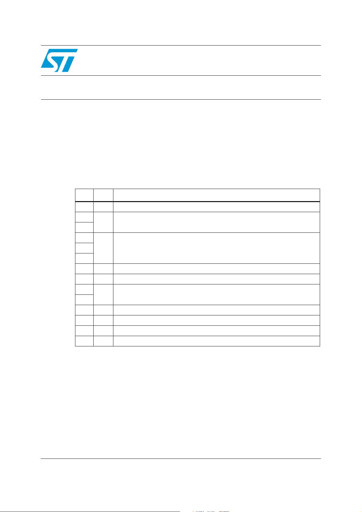
The part numbering scheme consists of a maximum of 13 digits grouped into nine fields (A
to H) as shown in Table 1: Serial EEPROM part numbering scheme on page 1<Blue>Table
1.
Fields A to C represent the product identifiers and fields D to H the product options. The “-”
character is used to separate the identifiers from the options.
Table 1. Serial EEPROM part numbering scheme
Digit Field Use
1st A Product line (“M” = memory)
2nd
3rd
4th
B Device type (Product family)
C Device function (Memory capacity)5th
6th
7th - Dash, to separate the product number identifiers from the product option designators
8th D Operating range (V
9th
E Package type
10th
11th F Device grade (Temperature range)
12th G Option
13th H Plating technology
14th /J Die process
CC
)
An additional “/” followed by two digits are used by ST to aid traceability, and might appear
on some documents at the bottom of the Ordering information scheme table under Process.
This information offers the die and technology references (for temperature range 3 devices)
and can be ignored for temperature range 6 devices.
July 2010 ID 5663 Rev 4 1/5
www.st.com
Page 2
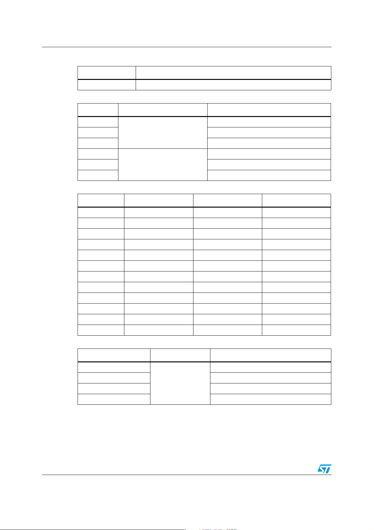
Table 2. Field A, 1st character, product line
Product line code Product line type
M Memory
Table 3. Field B, 2nd and 3rd characters, product family
Family code Memory type Family
AN626
93
24 I2C
Non-volatile memory
MICROWIRE
95 SPI
33
34 I
Application-specific memory
Non-volatile memory
MICROWIRE
2
C
35 SPI
Table 4. Field C, 4th, 5th and 6th characters, memory capacity
Capacity Microwire (M93) I²C (M24) SPI (M95)
1 Kb C46 C01 010
2 Kb C56 C02 020
4 Kb C66 C04 040
8 Kb C76 C08 080
16 Kb C86 C16 160
32 Kb - C32 320
64 Kb - C64 640
128 Kb - 128-B 128
256 Kb - 256-B 256
512 Kb - 512 512
1 Mb - M01 M01
2 Mb - M02 M02
Table 5. Field D, 8th character, VCC range
Voltage range code Memory Voltage range
Blank
W 2.5 V to 5.5 V
Serial EEPROMs
R 1.8 V to 5.5 V
F 1.7 V to 5.5 V
2/5 ID 5663 Rev 4
4.5 V to 5.5 V
Page 3

AN626
Table 6. Field E, 9
th
and 10th characters, package (two letters used in every case)
Package code Package type
BN PSDIP8 standard
CS WLCSP (Chip scale package)
CT Thin WLCSP (Chip scale package)
DW TSSOP8
DS TSSOP8 3 × 3 mm (MSOP8)
MN SO8 narrow 0.150 mils
MW SO8 wide 0.200 mils
MB UFDFPN8 (MLP8)
CS WLCSP (chip scale package)
CT TWLSCP (thin chip scale package)
Table 7. Field F, 11th character, temperature range
Device grade Temperature range
1 0 °C to 70 °C
3
–40 °C to +125 °C, with a certified reliability flow tailored for the automotive
industry
6 –40 °C to +85 °C
Table 8. Field G, 12th, packing option
Option code Option
Blank Standard packing
T Tape and reel packing
Table 9. Field H, 13th, plating technology
Code Plating technology
®
P or G ECOPACK
Table 10. Field J, 14th, die process
(RoHS compliant)
Code Plating technology
G or S F6SP
B or P F6DP
AF8L
KF8H
For complete details of the correct product number, and ordering codes, for a specific
product, please contact your nearest ST sales office or distributor.
ID 5663 Rev 4 3/5
Page 4

Revision history AN626
Revision history
Table 11. Document revision history
Date Revision Changes
June-1998 1.0 First Issue.
15th digit concerning Plating option added in Ta bl e 1 : Se r i a l
22-Nov-2004 2.0
25-Apr-2008 3 Document reformatted. All tables updated.
19-Jul-2010 4
EEPROM part numbering scheme. Tables 3, 5, 5, 6 updated and
Table 9: Field H, 13th, plating technology added.
Table 1: Serial EEPROM part numbering scheme, Ta b l e 4: F i e l d C,
4th, 5th and 6th characters, memory capacity, and Ta bl e 6 : F i el d E ,
th
and 10th characters, package (two letters used in every case)
9
updated. Table 10: Field J, 14th, die process added.
4/5 ID 5663 Rev 4
Page 5

AN626
Please Read Carefully:
Information in this document is provided solely in connection with ST products. STMicroelectronics NV and its subsidiaries (“ST”) reserve the
right to make changes, corrections, modifications or improvements, to this document, and the products and services described herein at any
time, without notice.
All ST products are sold pursuant to ST’s terms and conditions of sale.
Purchasers are solely responsible for the choice, selection and use of the ST products and services described herein, and ST assumes no
liability whatsoever relating to the choice, selection or use of the ST products and services described herein.
No license, express or implied, by estoppel or otherwise, to any intellectual property rights is granted under this document. If any part of this
document refers to any third party products or services it shall not be deemed a license grant by ST for the use of such third party products
or services, or any intellectual property contained therein or considered as a warranty covering the use in any manner whatsoever of such
third party products or services or any intellectual property contained therein.
UNLESS OTHERWISE SET FORTH IN ST’S TERMS AND CONDITIONS OF SALE ST DISCLAIMS ANY EXPRESS OR IMPLIED
WARRANTY WITH RESPECT TO THE USE AND/OR SALE OF ST PRODUCTS INCLUDING WITHOUT LIMITATION IMPLIED
WARRANTIES OF MERCHANTABILITY, FITNESS FOR A PARTICULAR PURPOSE (AND THEIR EQUIVALENTS UNDER THE LAWS
OF ANY JURISDICTION), OR INFRINGEMENT OF ANY PATENT, COPYRIGHT OR OTHER INTELLECTUAL PROPERTY RIGHT.
UNLESS EXPRESSLY APPROVED IN WRITING BY AN AUTHORIZED ST REPRESENTATIVE, ST PRODUCTS ARE NOT
RECOMMENDED, AUTHORIZED OR WARRANTED FOR USE IN MILITARY, AIR CRAFT, SPACE, LIFE SAVING, OR LIFE SUSTAINING
APPLICATIONS, NOR IN PRODUCTS OR SYSTEMS WHERE FAILURE OR MALFUNCTION MAY RESULT IN PERSONAL INJURY,
DEATH, OR SEVERE PROPERTY OR ENVIRONMENTAL DAMAGE. ST PRODUCTS WHICH ARE NOT SPECIFIED AS "AUTOMOTIVE
GRADE" MAY ONLY BE USED IN AUTOMOTIVE APPLICATIONS AT USER’S OWN RISK.
Resale of ST products with provisions different from the statements and/or technical features set forth in this document shall immediately void
any warranty granted by ST for the ST product or service described herein and shall not create or extend in any manner whatsoever, any
liability of ST.
ST and the ST logo are trademarks or registered trademarks of ST in various countries.
Information in this document supersedes and replaces all information previously supplied.
The ST logo is a registered trademark of STMicroelectronics. All other names are the property of their respective owners.
© 2010 STMicroelectronics - All rights reserved
STMicroelectronics group of companies
Australia - Belgium - Brazil - Canada - China - Czech Republic - Finland - France - Germany - Hong Kong - India - Israel - Italy - Japan -
Malaysia - Malta - Morocco - Philippines - Singapore - Spain - Sweden - Switzerland - United Kingdom - United States of America
www.st.com
ID 5663 Rev 4 5/5
 Loading...