

Page 1
AN604
Application note
Calculation of conduction losses in a power rectifier
Introduction
This application note explains how to calculate conduction losses in a power diode by taking
into account the forward voltage dependence on temperature and the current waveform.
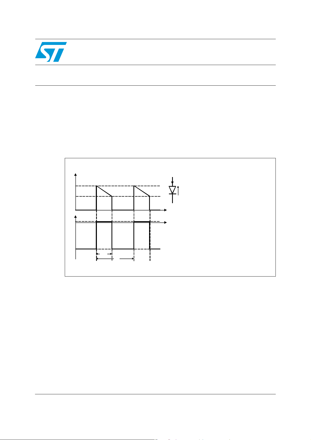
The ideal current and voltage waveforms of an ultrafast diode in a power supply system
during a switching cycle are shown in Figure 1.
Figure 1. Ideal current and voltage waveforms of a diode in a switch mode power
supply
I
(t)
D
I
Max
I
Min
ID(t)
VD(t)
F Switching frequency
sw
0
V
(t)
D
V
F
0
V
R
·T
δ
sw
T
sw
t
t
T Switching period
sw
Duty cycle
δ
T Duration of diode conduction
δ·
sw
I Maximum forward current
max
I Minimum forward current
min
V Forward voltage
F
V Reverse voltage
R
The conduction losses in a diode appear when the diode is in forward conduction mode due
to the on-state voltage drop (V
). Most of the time the conduction losses are the main
F
contributor to the total diode power losses and the junction temperature rising. This is the
reason why it is important to accurately estimate them.
August 2011 Doc ID 3607 Rev 3 1/12
www.st.com
Page 2

Contents AN604
Contents
1 Diode forward characteristics . . . . . . . . . . . . . . . . . . . . . . . . . . . . . . . . . 3
1.1 Junction temperature dependence . . . . . . . . . . . . . . . . . . . . . . . . . . . . . . . 3
1.2 Diode forward characteristics modeling: V
), RD(Tj) . . . . . . . . . . . . . . . 3
T0(Tj
2 Conduction losses: basic equations . . . . . . . . . . . . . . . . . . . . . . . . . . . . 6
2.1 Application parameters: average and rms currents . . . . . . . . . . . . . . . . . . 6
3 An application example . . . . . . . . . . . . . . . . . . . . . . . . . . . . . . . . . . . . . . 8
3.1 Average and rms current calculation . . . . . . . . . . . . . . . . . . . . . . . . . . . . . 9
3.2 V
3.3 Conduction losses expression . . . . . . . . . . . . . . . . . . . . . . . . . . . . . . . . . 10
(Tj) and RD (Tj) calculation . . . . . . . . . . . . . . . . . . . . . . . . . . . . . . . . . 9
T0
4 Revision history . . . . . . . . . . . . . . . . . . . . . . . . . . . . . . . . . . . . . . . . . . . 11
2/12 Doc ID 3607 Rev 3
Page 3
AN604 Diode forward characteristics
1 Diode forward characteristics
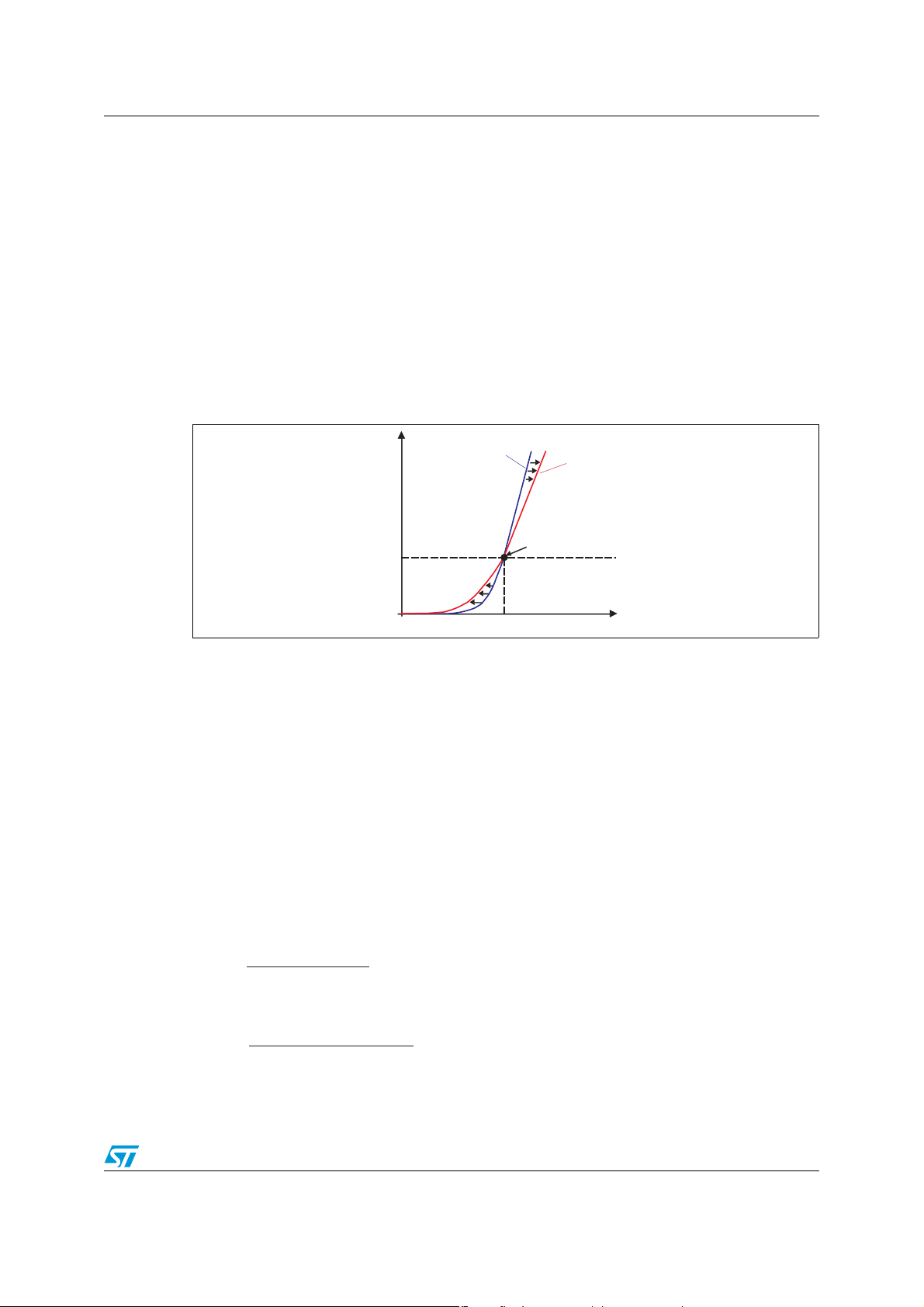
1.1 Junction temperature dependence
For two different junction temperatures, the current versus forward voltage curves cross at a
current level point I
the temperature coefficient α
higher, the temperature coefficient becomes positive. This behavior is shown in Figure 2.
For Schottky and bipolar diodes, I
SiC and GaN technologies, I
0, the forward voltage and the conduction losses decrease when the junction temperature
increases.
, depending on the diode technology. When the current is lower than Ic,
c
of the forward voltage is negative. When the current is
VF
is high and the working area corresponds to αVF < 0. For
c
is low and the αVF can be positive or negative. When of αVF <
c
Figure 2. Forward (I
) characteristics of a diode
F,VF
I
F
T
j1
I
c
0
αVF> 0
αVF= 0
αVF< 0
T
j2>Tj1
V
F
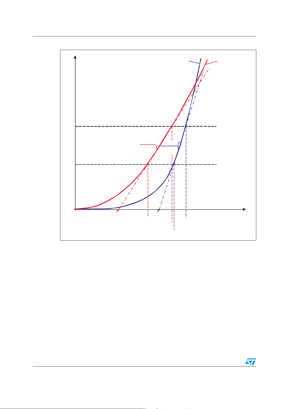
1.2 Diode forward characteristics modeling: VT0(Tj), RD(Tj)
Forward characteristics (IF and VF) can be modeled by a straight line defined by a threshold
voltage V
levels (I
Equation 1
Equation 2
, and a dynamic resistance RD. VT0 and RD are calculated for 2 forward current
T0
, IF2) for a given junction temperature as shown in Figure 3. Thus we can write:
F1
I)(TR)(TV)T,(IV ⋅+=
FjDjT0j1FF
1
I)(TR)(TV)T,(IV ⋅+=
FjDjT0j2FF
2
Using Equations 1 and 2, we obtain V
Equation 3
)(TR
=
jD
−
II
−
F
F
2
)T,(IV)T,(IV
j1FFj2FF
1
Equation 4
I)T,(IVI)T,(IV
⋅−⋅
Fj1FF
)(TV
=
jT0
2
II
−
F
F
1
2
Fj2FF
1
Doc ID 3607 Rev 3 3/12
) and RD(Tj) expressions:
T0(Tj
Page 4
Diode forward characteristics AN604
Figure 3. VT0(Tj) and RD(Tj) parameters
I
F
I
F2
T
jRef2
> T
jRef1
VF(IF,T
jRef1
)
VF(IF,T
jRef2
)
1
TR
jref2D
I
F1
0
and RD are given in each ST diode datasheet. In most cases they are calculated at
V
T0
125 °C with maximum V
VT0(T
) VT0(T
jRef2
VF(I
F1,TjRef2
values for IF1 = I
F
)
V
F(IF2,TjRef2
F(AV)
1
)(
TR
jref1D
)
jRef1
)
V
and IF2 = 2· I
)(
VF(IF2,T
F(IF1,TjRef1
F(AV)
jRef1
)
, where I
)
V
is the
F(AV)
average forward current rating of the diode. For a quick calculation these values can be
used. For more accurate estimation, R
and VT0 must be calculated using the specific
D
application conditions. See the example in Chapter 3.
F
4/12 Doc ID 3607 Rev 3
Page 5

AN604 Diode forward characteristics
For any junction temperature VT0(Tj), RD(Tj) and the forward voltage drop VF(IF,Tj) can be
calculated as follow:
Equation 5
()
)(TV)(TV
α
VjRef1T0jT0
TT
−⋅+=
T0
jRef1j
Equation 6
()
TTα)(TR)(TR −⋅+=
RjRef1DjD
D
jRef1j
Equation 7
()()
TT)T,(IV)T,(IV
VjRef1jjRef1FFjFF
T0
I
αα
⋅+⋅−+=
FDR
Note:
Where α
T
and T
jref1
and α
VTO
. A common choice of T
jref2
are thermal coefficients calculated from the 2 reference temperatures:
RD
jref1
and T
is 25 °C and 125 °C. These thermal
jref2
coefficients are calculated with the following equations:
Equation 8
α
V
T0
() ()
=
TVTV
−
jref1T0jref2T0
TT
−
jref1jref2
Equation 9
α
R
VT0
() ()
=α
D
< 0 and
TRTR
−
jref1Djref2D
TT
−
jref1jref2
α
> 0 whatever the diode technology.
RD
Doc ID 3607 Rev 3 5/12
Page 6

Conduction losses: basic equations AN604
2 Conduction losses: basic equations
Conduction losses are the average dissipated power in the diode during the forward
conduction phase given in Equation 10:
Equation 10
T
sw
1
)(TP
jCOND
T
sw
∫
0
()
FjFF
dt(t)IT,IV
⋅⋅=
Equation 10 can also be written as follows:
Equation 11
2
I)(TRI)(TV)(TP ⋅+⋅=
F(rms)jDF(av)jT0jCOND
Where I
is the forward average current and I
F(AV)
F(RMS)
is the forward root mean square
current flowing through the diode.
Note: In case of a square waveform, a short formula can be used to calculate conduction losses:
Equation 12
δI)T,(IV)(TP
⋅⋅=
F(AV)jFFjCOND
2.1 Application parameters: average and rms currents
The average and rms currents are different for each application condition. They can be
calculated using Equations 12 (average current) and 13 (rms current).
Equation 13
I
AVF
T
sw
1
()
⋅=
)(
T
dttI
∫
0Fsw
Equation 14
T
sw
1
2
()
⋅=
I
)(
RMSF
T
sw
dttI
F
∫
0
Figure 4 presents simplified expression of average and rms currents of commonly observed
waveforms in a power rectifier. In most cases, these waveforms can be used for a rough
estimation.
6/12 Doc ID 3607 Rev 3
Page 7

AN604 Conduction losses: basic equations
Figure 4. Average and rms currents of commonly observed waveforms
Square waveform
(t)
I
D
I
Max
Trapezoidal waveform
ID(t)
I
Max
I
Min
0
δ•T
sw
T
sw
·=
II
MaxAVF
)(
δδ·=
II
MaxRMSF
)(
Half period sinusoidal waveform
ID(t)
I
Max
0
δ•T
sw
T
sw
I2
Max
·=
I
AVF
)(
δ
π
δ
·=
II
MaxRMSF
)(
2
t
0
δ•T
sw
T
sw
+
II
MinMax
2
Max
·
δ
2
2
Min
3
=
I
AVF)()(
=
I
RMSF
t
×++
IIII
MinMax
δ
·
Triangular waveform
I
(t)
D
I
Max
t
0
δ·T
sw
T
sw
I
I
Max
·=
AVF
)(
δ
2
δ
II
·=
MaxRMSF
)(
3
t
Doc ID 3607 Rev 3 7/12
Page 8

An application example AN604
3 An application example
Let us consider the example of a 90 W notebook adapter. This is a flyback converter
(Figure 5) working in continuous mode. The output voltage V
output current is 4.7 A. The rectifier diode is an ST power Schottky STPS30M100S. Figure 6
shows the ideal waveforms of the diode: I
= 4 A, I
Min
= 11.8 A and δ = 0.6.
Max
Let us calculate the maximum conduction losses in the diode for this application.
Figure 5. Flyback converter
is 19 V and the maximum
out
V
in I
Snubber
STPS30M100S
load
V
out
AC Line
Control
Figure 6. Ideal current and voltage waveforms of the diode in the flyback converter.
ID(t)
I
Max
I
Min
VD(t)
0
V
F
0
t
t
V
R
δ·T
sw
T
sw
8/12 Doc ID 3607 Rev 3
Page 9

AN604 An application example
3.1 Average and rms current calculation
The first step is the calculation of the average and rms currents.
The forward average current is the output current: I
As illustrated in Figure 6, the forward current has a trapezoidal shape. The formula to
calculate the rms current of trapezoidal waveform is given in Figure 4. I
Equation 15
22
3
411.8411.8
⋅++
6.4 A0.6
=⋅
I
F(RMS)
()()
=
3.2 VT0 (Tj) and RD (Tj) calculation
The second step is the calculation of VT0 (Tj) and RD (Tj) in the application condition range.
Figure 7. STPS30M100S forward voltage drop versus forward current
I
FM
T = 125 °C
j
(Maximum values)
F(AV)
= I
load
= 4.7 A.
F(RMS)
is then:
T = 125 °C
j
(Typical values)
I
= 11.8A
Max
I
= 4A
Min
0.43V
T
= 25 °C and T
jref1
values of V
F
at I
Min
= 125 °C. To calculate maximum conduction losses, read maximum
jref2
and I
in Figure 7. This figure is available in the STPS30M100S
Max
datasheet. These values are summarized in Table 1.
Table 1. V
IF (A) V
I
= 4 0.52 0.43
Min
= 11.8 0.63 0.55
I
Max
F(Max)
values at I
and I
Min
F(Max)(IF
Max
, 25 °C) (V) V
0.52V
0.55V
T = 25 °C
j
(Maximum values)
0.63V
F(Max)(IF
, 125 °C) (V)
Doc ID 3607 Rev 3 9/12
Page 10

An application example AN604
From Equations (3), (4), (8) and (9) calculate VT0(T
α
and αRD. Calculated values of these parameters are summarized in Table 2.
VT0
Table 2. V
T
(°C) VT0 (V) RD (mΩ) α
jref
= 25 0.464 14.123
T
jref1
T
= 125 0.368 15.406
jref2
, RD, α
T0
, and αRD parameters
VT0
From Equations 5 and 6 we can write VT0(Tj) and RD(Tj) as follow:
Equation 16
-6
T10951.358-0.487)(TV ⋅×=
jT0
Equation 17
jD
j
-6-3
T1012.8391013.802)(TR ⋅×+×=
j
3.3 Conduction losses expression
From Equations 7, 15 and 16 the expression for maximum conduction losses is then:
Equation 18
jCOND(Max)
-3
T103.9872.866)(TP ⋅×+=
j
jref1
), VT0(T
VT0
-951.358×10
), RD(T
jref2
jref1
(V·°C-1) α
-6
), RD(T
RD
jref2
(Ω·°C-1)
12.839×10
),
-6
Finally, let us plot the value of conduction losses in the diode as a function of the junction
temperature (Figure 8).
Figure 8. Maximum conduction losses versus junction temperature
P(T)
COND(Max) j
3.0W
2.8W
2.6W
2.4W
2.2W
T
2.0W
25°C 35°C 45°C 55°C 65 °C 75°C 85°C 95°C105°C115°C 125 °C
j
10/12 Doc ID 3607 Rev 3
Page 11

AN604 Revision history
4 Revision history
Table 3. Document revision history
Date Revision Changes
Aug-1993 1 Initial release
03-May-2004 2 Stylesheet update. No content change
24-Aug-2011 3 Completely revised for currently available products.
Doc ID 3607 Rev 3 11/12
Page 12

AN604
Please Read Carefully:
Information in this document is provided solely in connection with ST products. STMicroelectronics NV and its subsidiaries (“ST”) reserve the
right to make changes, corrections, modifications or improvements, to this document, and the products and services described herein at any
time, without notice.
All ST products are sold pursuant to ST’s terms and conditions of sale.
Purchasers are solely responsible for the choice, selection and use of the ST products and services described herein, and ST assumes no
liability whatsoever relating to the choice, selection or use of the ST products and services described herein.
No license, express or implied, by estoppel or otherwise, to any intellectual property rights is granted under this document. If any part of this
document refers to any third party products or services it shall not be deemed a license grant by ST for the use of such third party products
or services, or any intellectual property contained therein or considered as a warranty covering the use in any manner whatsoever of such
third party products or services or any intellectual property contained therein.
UNLESS OTHERWISE SET FORTH IN ST’S TERMS AND CONDITIONS OF SALE ST DISCLAIMS ANY EXPRESS OR IMPLIED
WARRANTY WITH RESPECT TO THE USE AND/OR SALE OF ST PRODUCTS INCLUDING WITHOUT LIMITATION IMPLIED
WARRANTIES OF MERCHANTABILITY, FITNESS FOR A PARTICULAR PURPOSE (AND THEIR EQUIVALENTS UNDER THE LAWS
OF ANY JURISDICTION), OR INFRINGEMENT OF ANY PATENT, COPYRIGHT OR OTHER INTELLECTUAL PROPERTY RIGHT.
UNLESS EXPRESSLY APPROVED IN WRITING BY TWO AUTHORIZED ST REPRESENTATIVES, ST PRODUCTS ARE NOT
RECOMMENDED, AUTHORIZED OR WARRANTED FOR USE IN MILITARY, AIR CRAFT, SPACE, LIFE SAVING, OR LIFE SUSTAINING
APPLICATIONS, NOR IN PRODUCTS OR SYSTEMS WHERE FAILURE OR MALFUNCTION MAY RESULT IN PERSONAL INJURY,
DEATH, OR SEVERE PROPERTY OR ENVIRONMENTAL DAMAGE. ST PRODUCTS WHICH ARE NOT SPECIFIED AS "AUTOMOTIVE
GRADE" MAY ONLY BE USED IN AUTOMOTIVE APPLICATIONS AT USER’S OWN RISK.
Resale of ST products with provisions different from the statements and/or technical features set forth in this document shall immediately void
any warranty granted by ST for the ST product or service described herein and shall not create or extend in any manner whatsoever, any
liability of ST.
ST and the ST logo are trademarks or registered trademarks of ST in various countries.
Information in this document supersedes and replaces all information previously supplied.
The ST logo is a registered trademark of STMicroelectronics. All other names are the property of their respective owners.
© 2011 STMicroelectronics - All rights reserved
STMicroelectronics group of companies
Australia - Belgium - Brazil - Canada - China - Czech Republic - Finland - France - Germany - Hong Kong - India - Israel - Italy - Japan -
Malaysia - Malta - Morocco - Philippines - Singapore - Spain - Sweden - Switzerland - United Kingdom - United States of America
www.st.com
12/12 Doc ID 3607 Rev 3
 Loading...