

AN593
ST621x/2x ST624x
ST626x/9x
PA6
PA5
OSCin
PA7
RESETRESET
PB7
OSCin
PB5
PB6
Not used
RESET
PB2
OSCin
PB0
PB3
Connect to:
1
3
5
7
9
11
13
NC
14
12
10
8
6
4
2
16
HE10
TOP VIEW
Connect to ALL
VR01856
NC
NC
NC
15
Serial in
Serial out
V
SS
of
Application Board
VDD Optional
VPP / TMVPP / TM
V
PP
/ TM
PC6
PC5
PC7
RESET
ST628x
OSCin
Not used
Not used
Not used
V
PP
/ TM
APPLICATION NOTE
ST62 in-circuit programming
In-circuit programming feature
The in-circuit programming process allows programming or reading of the non volatile memory of
an ST62 device already fixed on the application
board. This feature applies both to the EPROM
memory containing the user ROM (Executable
code and constants) and to the EEPROM content
(Non volatile data). The capability to program
memory locations initially unprogrammed and ac
cess the user ROM content allows a wide range of
applications enhancement: Storage of informa
tions after a maintenance operation on field, follow-up of the software revision on field, update of
non volatile data space, In addition, this in-circuit
programming process limits the handling on com
plex packages like PQFP since the handling cycles for the programming is suppressed and only
the handling for the soldering on PCB is needed.
This note provides information on the steps required in order to perform in-circuit programming
of ST62Exxx EPROM or OTP devices for both onchip EPROM and EEPROM.
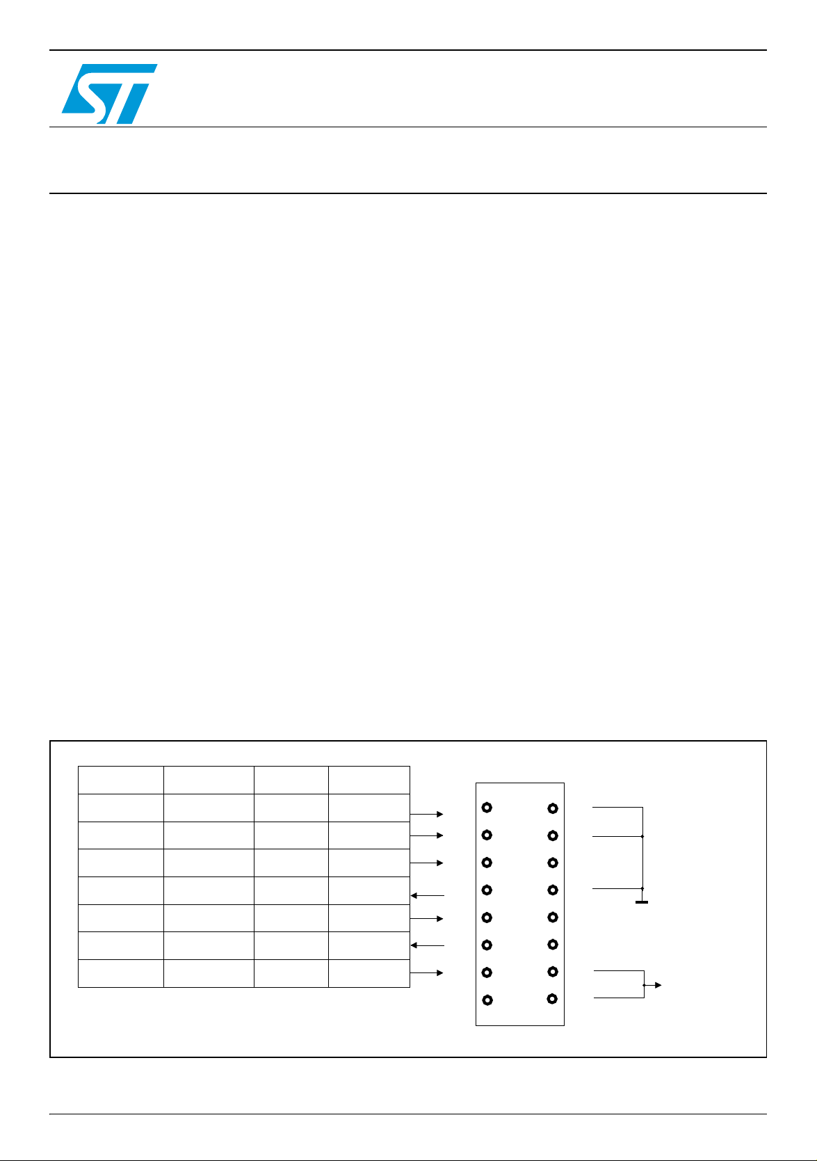
In-circuit programming procedure
During the in-circuit programming progress, the
application board is used as remote socket for the
programming tool and the programming process
and software remains unchanged. The connection
of the application board to/from the programming
tool is made through a 16 pin cable plugged into a
16 pin connector (8x2 header HE10). That 16 pin
connector has to be provided by the designer on
the application board.
The connections between the 16 pins connector
and the ST62 are summarized below:
Note: The connection to the pin3 of the connector
is not necessary if a high voltage level is guaran
teed by the application design (See Application
design guidelines)
The VDD connection is optional depending whether or not the application supply can be disconnected. If the application supply is disconnected, it is
possible to supply the application board through
the pins 14 and 16 of the connector as long as the
total load current does not exceed 100mA and the
capacitive load is lower than 50F. In the opposite,
if the application board keeps its own supply, the
supply value must be set at 5V in order to be com
patible with the signal levels to/from the programming tool.
Figure 1. 16-pin PCB Socket Connection
June 2008 Rev 2 1/4
ST62 in-circuit programming
Application design guidelines
Some care has to be taken in the application design in order to be compatible with the in-circuit
programming capability.
1) The OSCin pin is used to synchronize the programming operations with a clock sent by the programming tool through the 16 wire cable. This
node must be directly tied to the relevant pin of the
16 wire cable. No isolation is needed as long as a
quartz crystal or a ceramic resonator is used in the
application. If an external clock generator is used
in the application, it has to be disconnected during
the in-circuit programming operation.
2) The RESET pin is used by the programming
tool to control the programming mode entry. Then
a direct connection to the device, and a correct
isolation from other signals of the application is
mandatory to prevent any voltage contention. It
means that a direct connection to VDD, GND or
any other signal has to be avoided. On the contra
ry, these pins can be connected to another CMOS
input, a 2 Kohms pull-up or left open (Internal pullup). The capacitive load on the RESET pin should
not exceed 1F.
3) The pin 1 and 7 of the 16 wire cable are used to
establish the communication between the programming tool and the device. Then a direct connection to the device, and a correct isolation from
other nodes of the application is mandatory to prevent any voltage contention. It means that any direct connection to VDD, GND or an output has to
be avoided. On the contrary, these pins can be
connected to a CMOS input, a 2 Kohms pull-up, a
10Kohms pull-down or left open (Internal pull-up).
If the pin 3 of the 16 pin connector is tied to the
ST62 MCU, the same concerns apply. 4) Some
I/O pins are not connected to the 16 wire cable
and must be set at high level during the program
ming operation. This is normally achieved by the
RESET signal sent by the programming tool
through the 16 wire cable, setting the I/O lines as
input with an internal 300 Kohms pull-up. In order
to keep at high level these I/O lines, a direct con
nection of these pins to GND or to any other signal
at low (even temporarily) voltage level has to be
avoided. Only connections to another CMOS in
put, an external pull-up or a 10 MOhms pull down
is allowed.
The following table summarizes the signal to be
kept at high voltage level.
ST621X/2X ST624X ST626X ST628X
PB3 PB0 PB6 PB3
PB5 * PA5 * PB0 * PC5*
*: If not directly biased through the pin 3 of the 16
pin connector.
5) The pin Vpp/TM can not be directly tied to GND
on the application in order to do not conflict with
the biasing issued by the programming tool
through the pin 13 of the connector. Instead it
should be pulled down by a resistor with a mini
mum value of 10 Kohms. It is also mandatory to
add a 100nF ceramic capacitor between Vpp/TM
and Vss.
2/4

Revision history
Table 1. Revision history
Date Revision Description of changes
March 1993 1 Initial release
13-June-2008 2 Logo modified
ST62 in-circuit programming
3/4

ST62 in-circuit programming
Please Read Carefully:
Information in this document is provided solely in connection with ST products. STMicroelectronics NV and its
subsidiaries (“ST”) reserve the right to make changes, corrections, modifications or improvements, to this document, and
the products and services described herein at any time, without notice.
All ST products are sold pursuant to ST’s terms and conditions of sale.
Purchasers are solely responsible for the choice, selection and use of the ST products and services described herein,
and ST assumes no liability whatsoever relating to the choice, selection or use of the ST products and services described
herein.
No license, express or implied, by estoppel or otherwise, to any intellectual property rights is granted under this
document. If any part of this document refers to any third party products or services it shall not be deemed a license grant
by ST for the use of such third party products or services, or any intellectual property contained therein or considered as
a warranty covering the use in any manner whatsoever of such third party products or services or any intellectual property
contained therein.
UNLESS OTHERWISE SET FORTH IN ST’S TERMS AND CONDITIONS OF SALE ST DISCLAIMS ANY EXPRESS
OR IMPLIED WARRANTY WITH RESPECT TO THE USE AND/OR SALE OF ST PRODUCTS INCLUDING WITHOUT
LIMITATION IMPLIED WARRANTIES OF MERCHANTABILITY, FITNESS FOR A PARTICULAR PURPOSE (AND
THEIR EQUIVALENTS UNDER THE LAWS OF ANY JURISDICTION), OR INFRINGEMENT OF ANY PATENT,
COPYRIGHT OR OTHER INTELLECTUAL PROPERTY RIGHT.
UNLESS EXPRESSLY APPROVED IN WRITING BY AN AUTHORIZED ST REPRESENTATIVE, ST PRODUCTS ARE
NOT RECOMMENDED, AUTHORIZED OR WARRANTED FOR USE IN MILITARY, AIR CRAFT, SPACE, LIFE
SAVING, OR LIFE SUSTAINING APPLICATIONS, NOR IN PRODUCTS OR SYSTEMS WHERE FAILURE OR
MALFUNCTION MAY RESULT IN PERSONAL INJURY, DEATH, OR SEVERE PROPERTY OR ENVIRONMENTAL
DAMAGE. ST PRODUCTS WHICH ARE NOT SPECIFIED AS "AUTOMOTIVE GRADE" MAY ONLY BE USED IN
AUTOMOTIVE APPLICATIONS AT USER’S OWN RISK.
Resale of ST products with provisions different from the statements and/or technical features set forth in this document
shall immediately void any warranty granted by ST for the ST product or service described herein and shall not create or
extend in any manner whatsoever, any liability of ST.
ST and the ST logo are trademarks or registered trademarks of ST in various countries.
Information in this document supersedes and replaces all information previously supplied.
The ST logo is a registered trademark of STMicroelectronics. All other names are the property of their respective owners.
© 2008 STMicroelectronics - All rights reserved
STMicroelectronics group of companies
Australia - Belgium - Brazil - Canada - China - Czech Republic - Finland - France - Germany - Hong Kong - India - Israel
- Italy - Japan - Malaysia - Malta - Morocco - Singapore - Spain - Sweden - Switzerland - United Kingdom - United States
of America
www.st.com
4/4
 Loading...