

AN592
Application note
PLL generation using ST62 auto-reload timer
INTRODUCTION
This note describes how to generate a digital signal locked in phase and frequency (PLL) with a
calibrated delay starting from an active edge on the Auto-reload timer input pin.
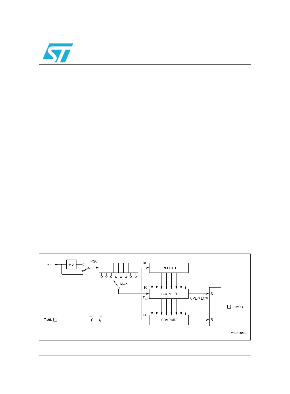
Auto-reload timer description
This timer is an 8 bit timer/counter with prescaler. It includes auto-reload PWM, capture and
compare capability with one input and one output pins. It can be controlled by the following registers (8 bit):
Mode Control Register (MC)
-
Status registers (SC0, SC1)
-
Load register (LR)
-
Incremental counter register (TC)
-
Compare register (CP)
-
Reload/Capture register (RC)
-
It can also wake-up the MCU from wait mode and exit from stop mode if an external event is
present on the input pin. The prescaler ratio can be programmed to choose the timer input frequency F
Example:
The TIMIN input receives a 15 kHz digital signal. We want to generate a phase-locked 15 kHz
digital signal with a falling edge delayed 19μs from the input rising edge, and a duty cycle of
75%. The CPU quartz frequency is 8 MHz.
(see Table 1).
IN
Figure 1. Auto-reload Timer Block Diagram
June 2008
Rev 2 1/5
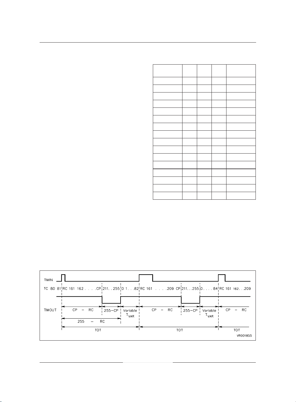
PLL Generation using ARTimer
The Figure 2 shows the TIMOUT signal generated in “load on external edge” mode,
given the above TIMIN signal: on TIMIN rising edge, the TC count register is loaded with
the value contained in RC register (160 in
this example). The timer will resume counting from value 160. When the compare value
(210 in this example) is reached, the
TIMOUT signal goes down. The timer keeps
counting until the overflow (255) is reached.
At this point, signal TIMOUT rises again. The
timer keeps counting from 0 until next active
edge on TIMIN. At this time, TC is loaded
again with the RC value (160) and so on...
The delay from TIMIN edge to TIMOUT falling edge is given by CP-RC (multiplied by the
TC register clock period Fin). The low level
duration on TIMOUT is given by 255 - CP.
The remaining of the TIMOUT period is variable, and will adjust to the TIMIN period:
small variations of TIMIN period will be absorbed by a variation of T
. The following
VAR
rule must be respected in order to get the
proper output signal:
The variable time Tvar must stay smaller
than CP, (otherwise the falling edge on
TIMOUT occurs before rising edge on
TIMIN) and larger than 0 (otherwise the rising edge on TIMOUT never occurs).
In other words, the period of input TIMIN
(TOT in terms of TC clock cycles) must meet
the following requirement:
255-RC<TOT<255-RC+CP
Table 1. Prescaler Programming Ratio
Bit 0
Reg. SC1
0 000 1
0 001 2
0 010 4
0 011 8
0 100 16
0 101 32
0 110 64
0 111 128
1 000 3
1 001 6
1 010 12
1 011 24
1 100 48
1 101 96
1 110 192
1 111 384
PS2 PS1 PS0
PRESCALER
Ratio
Coming back to our example, let’s calculate
the timer settings:
The input period is Tin = 1/15 kHz = 66.7μs
Calculation of the prescaler ratio:
We want the best possible resolution, e.g.
the smaller possible prescaler ratio: we
would like the TC counter to count up to the
Figure 2. TIMOUT signal
Note: All numbers are decimal
2/5

PLL Generation using ARTimer
highest number: 255 (for best resolution). In this case 66.7μs / 255 = 0.26μs is the smallest TC
clock period that we can use. With a prescaler ratio of 1, the TC clock period is 1/8MHz = 0.125
μs. So we need a prescaler ratio of 3, giving a TC clock period of 3/8 MHz = 0.375μs. This is the
elementary incrementing time of the TC counter, which gives the resolution of the phase shift
and of the low level on TIMOUT (the TC counter is incremented with a clock F
= 1/0.375μs=
IN
2667kHz).
The desired delay is 19μs: CP - RC = 19μs /0.375μs = 50.67.
The TIMIN period is:
TOT = 66.7μs / 0.375 μs = 177.78.
The duty cycle is: 0.25 = (255 - CP)/TOT
Rounding the decimals, this gives:
RC = 160; CP = 210; TOT = 178
The variable time T
VAR
is: T
=TOT-255+RC=83
VAR
The condition is met: Tvar is positive and smaller than CP: (255 - 160) < 178 < (255 - 160 + 210)
The TIMOUT signal will remain correct and stable as long as this condition is met, even if the in-
put frequency varies:
The input frequency limits for output correctness are:
(255 - 160) x 0.375μs<T
(255 - 160 + 210) x 0.375μs
IN <
The output signal will remain locked in phase and frequency as long as the input signal TIMIN
is in the range:
8.7kHz < TIMIN frequency < 28kHz
Of course, it is also possible to modify by software the 19μs delay and the 75% duty cycle, for
example by measuring repetitively an error voltage with the A/D converter and calculating the
modified delay or duty cycle.
Program example
;**************** A-R Timer Register Set *******************
RC .def 0D9h,0FFh,0FFh ;reload/capture register
CP .def 0DAh,0FFh,0FFh ;compare register
MC .def 0D5h,0FFh,0FFh ;mode control register
SC0 .def 0D6h,0FFh,0FFh ;status/control register 0
SC1 .def 0D7h,0FFh,0FFh ;status/control register 1
LR .def 0DBh,0FFh,0FFh ;load register
;============================================================
ldi CP, 210 ;compare register = 210d
ldi RC, 160 ;reload register = 160d
ldi SC1,00000101b ;clock source= CPU clock divided by 3
ldi MC, 11100011b ;load on TIMIN mode,interrupts disabled
;rising TIMIN edge active
;pull-up disabled, prescaler ratio = 1
;PWMOUT enabled, start timer
3/5

PLL Generation using ARTimer
Table 6. Revision history
Date Revision Description of changes
March 1993 1 Initial release
30-June-2008 2 Logo modified
4/5

Please Read Carefully:
PLL Generation using ARTimer
Information in this document is provided solely in connection with ST products. STMicroelectronics NV and its subsidiar
ies (“ST”) reserve the right to make changes, corrections, modifications or improvements, to this document, and the prod-
ucts and services described herein at any time, without notice.
All ST products are sold pursuant to ST’s terms and conditions of sale.
Purchasers are solely responsible for the choice, selection and use of the ST products and services described herein,
and ST assumes no liability whatsoever relating to the choice, selection or use of the ST products and services described
herein.
No license, express or implied, by estoppel or otherwise, to any intellectual property rights is granted under this docu-
ment. If any part of this document refers to any third party products or services it shall not be deemed a license grant by
ST for the use of such third party products or services, or any intellectual property contained therein or considered as a
warranty covering the use in any manner whatsoever of such third party products or services or any intellectual property
contained therein.
UNLESS OTHERWISE SET FORTH IN ST’S TERMS AND CONDITIONS OF SALE ST DISCLAIMS ANY EXPRESS OR IMPLIED WARRANTY WITH RESPECT TO THE USE AND/OR
SALE OF ST PRODUCTS INCLUDING WITHOUT LIMITATION IMPLIED WARRANTIES OF
MERCHANTABILITY, FITNESS FOR A PARTICULAR PURPOSE (AND THEIR EQUIVA-
LENTS UNDER THE LAWS OF ANY JURISDICTION), OR INFRINGEMENT OF ANY PAT-
ENT, COPYRIGHT OR OTHER INTELLECTUAL PROPERTY RIGHT.
UNLESS EXPRESSLY APPROVED IN WRITING BY AN AUTHORIZED ST REPRESENTA-
TIVE, ST PRODUCTS ARE NOT RECOMMENDED, AUTHORIZED OR WARRANTED FOR
USE IN MILITARY, AIR CRAFT, SPACE, LIFE SAVING, OR LIFE SUSTAINING APPLICA-
TIONS, NOR IN PRODUCTS OR SYSTEMS WHERE FAILURE OR MALFUNCTION MAY
RESULT IN PERSONAL INJURY, DEATH, OR SEVERE PROPERTY OR ENVIRONMENTAL
DAMAGE. ST PRODUCTS WHICH ARE NOT SPECIFIED AS “AUTOMOTIVE GRADE” MAY
ONLY BE USED IN AUTOMOTIVE APPLICATIONS AT USER’S OWN RISK.
Resale of ST products with provisions different from the statements and/or technical features set forth in this document
shall immediately void any warranty granted by ST for the ST product or service described herein and shall not create or
extend in any manner whatsoever, any liability of ST.
-
ST and the ST logo are trademarks or registered trademarks of ST in various countries.
Information in this document supersedes and replaces all information previously supplied.
The ST logo is a registered trademark of STMicroelectronics. All other names are the property of their respective owners.
© 2008 STMicroelectronics - All rights reserved
STMicroelectronics group of companies
Australia - Belgium - Brazil - Canada - China - Czech Republic - Finland - France - Germany -
Hong Kong - India - Israel - Italy - Japan - Malaysia - Malta - Morocco - Singapore - Spain -
Sweden - Switzerland - United Kingdom - United States of America
www.st.com
5/5
 Loading...