

AN576
APPLICATION NOTE
PCB LAYOUT OPTIMISATION
INTRODUCTION
Protection requirements are becoming more and more well known and are often defined by rules or standards. To satisfy these requirements, there is, in the majority of cases, a standard solution or a dedicated
product.
However, knowledge of the disturbances and the use of suitable protection devices are not sufficient in
themselves to solve the problem. In many applications, the correct design of the PCB layout is essential
for success.
Figure 1. Classical protection circuit
Track B
Track A
I
DEVICE
DISTURBANCE
SOURCE
INFLUENCE OF THE PROTECTION LOCATION
The circuit presented in Figure 1 shows the classical approach for the protection location. Here the protection device (see Note 1) is located close to the module to be protected. When a disturbance occurs on
the track A the TRANSIL P clamps the surge at a maximum voltage V
part.
During this clamping action there is a current through P and also in the track A. This phenomenon induces
a voltage on track B, where it is close to A. To avoid this undesirable parasitic overvoltage on track B, the
circuit of Figure 2 is recommended.
Note: 1. TRANSIL devices are used as examples throughout this document, but the same arguments are valid for TRISILS.
V
CL
P
TO BE
PROTECTED
and thus protects the sensitive
CL
REV. 2A - 3588
1/6May 2004
AN576
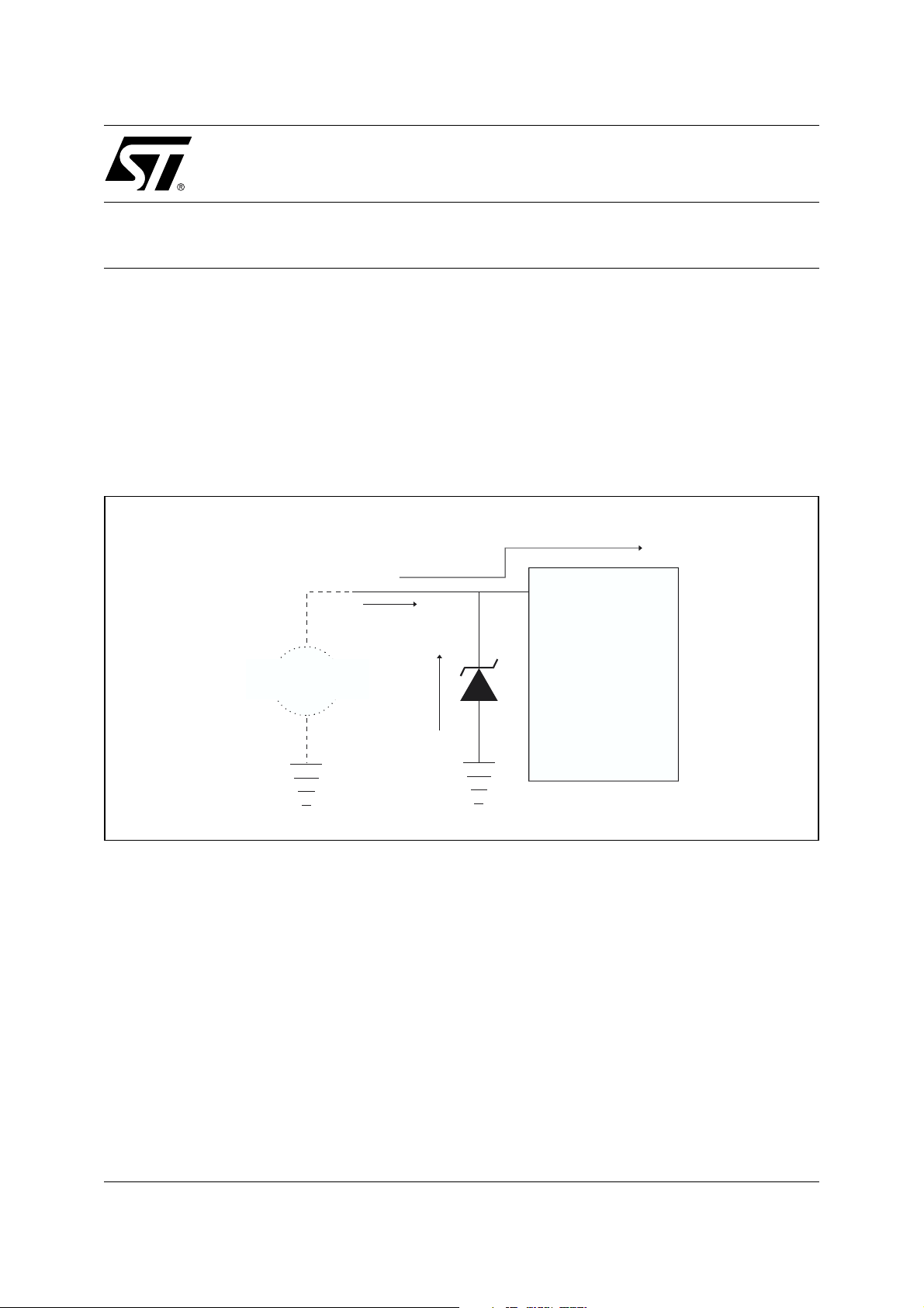
Figure 2. Recommended protection location
Track B
P
Track A
V
CL
DEVICE
TO BE
PROTECTED
I
DISTURBANCE
SOURCE
In this case the current due to the clamping phase of P remains located in the disturbance area and the
track B is not affected.
To summarize, it is recommended that the protection device is located as close as possible the disturbance source. For example, all the lines coming into the board ought to be protected close to the connector.
INFLUENCE OF THE PCB LAYOUT ON THE ESD PROTECTION
These days, printed circuit boards are often auto-routed by computer aided design and the track lengths
are not optimized.
Figure 3. Non-optimized LAYOUT for ESD
A
P
U
DISTURBANCE
SOURCE
B
DEVICE
TO BE
PROTECTED
Figure 3 shows the classical non-optimized layout. When a surge occurs the protection device P acts and
there is a clamping voltage V
across it. Due to the fast rise time of the ESD overvoltage there is a high
CL
di/dt between the points A and B. This di/dt generates, in the parasitic inductances located between A and
P and between B and P, overvoltages up to several hundred volts. So the applied voltage V across the
device to be protected is the sum of the clamping voltage and the voltage across the parasitic inductance:
thus the sensitive module is not protected.
2/6

AN576
In the case of Figure 4, the design topology is based on a 4 point circuit. When a surge occurs the Transil
clamps at Vcl and due to the design the di/dt effects remain on the left hand side of P. Therefore the voltage V seen by the sensitive device is roughly equal to V
Figure 4. Optimized layout for ESD
I
DISTURBANCE
SOURCE
N.B.: The surface mount family SOD6 and SOD15 are particularly suited to this kind of application.
P
V
CL
CL
.
DEVICE
TO BE
U
PROTECTED
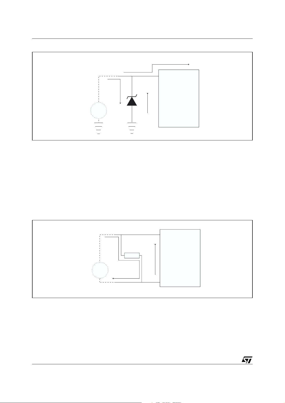
Figure 5. Printer circuit board protection against ESD with case
PRINTED BOARD
MODULE CASE
These days most inputs are protected against ESD (though not always effectively) and so the voltage between the lines and ground never exceeds dangerous values.
However, this does not prevent the total electrical potential from increasing, possibly resulting in sparks
between one point of the board and the module case. To avoid this problem we recommend a bidirectional
Transil (BZW04P37B) between the printed circuit board ground and the metallic parts of the case.
3/6

AN576
Figure 6. Distributed protection
DISTURBANCE
SOURCE
SENSITIVE PARTS
INPUT / OUTPUT
PRINTED BOARD
DISTRIBUTED PROTECTION
The printed circuit board shown in Figure 5 represents a general case. In this board the input/output lines
are protected close to the connector and overvoltages are cancelled close to the disturbance sources. The
other lines to be protected are the power supply wires which carry 3 kinds of disturbances:
– The overvoltages resulting from mains perturbations.
– The surges coming from the other boards supplied by these lines.
– The disturbances generated on the board by the normal operation of the resident module, for example
the di/dt due to the fast switching of a buffer.
To suppress these surges we suggest a powerful Transil (1.5 KE for example) close to the power supply
input on the board, and some lower power devices (e.g. BZW04) distributed around the board area.
CONCLUSION
Due to the parasitic inductance of PCB tracks, a protection device chosen purely according to disturbance
standards does not assure immunity from surges. Carefully designed PCB layout plus correct device selection from the STMicroelectronics range is essential to guarantee adequate protection.
4/6

REVISION HISTORY
Table 1. Revision History
Date Revision Description of Changes
March-1993 1 First Issue
3-May-2004 2 Stylesheet update. No content change.
AN576
5/6

AN576
Information furnished is believed to be accurate and reliable. However, STMicroelectronics assumes no responsibility for the consequences
of use of such information nor for any infringement of patents or other rights of third parties which may result from its use. No license is granted
by implication or otherwise under any patent or patent rights of STMicroelectronics. Specifications mentioned in this publication are subject
to change without notice. This publication supersedes and replaces all information previously supplied. STMicroelectronics products are not
authorized for use as critical components in life support devices or systems without express written approval of STMicroelectronics.
The ST logo is a registered trademark of STMicroelectronics.
All other names are the property of their respective owners
© 2004 STMicroelectronics - All rights reserved
STMicroelectronics GROUP OF COMPANIES
Australia - Belgium - Brazil - Canada - China - Czech Republic - Finland - France - Germany - Hong Kong - India - Israel - Italy - Japan -
Malaysia - Malta - Morocco - Singapore - Spain - Sweden - Switzerland - United Kingdom - United States
www.st.com
6/6
 Loading...