

Page 1
AN557
APPLICATION NOTE
EASY APPLICATION DESIGN WITH THE L4970A,
MONOLITHIC DC-DC CONVERTERS FAMILY
The L497XA series of high current switching regulator ICs exploit Multipower-BCD technology to
achieve very high output currents with low power dissipation – up to 10A in the Multiwatt power package
and 3.5A in a DIP package .
THE TECHNOLOGY
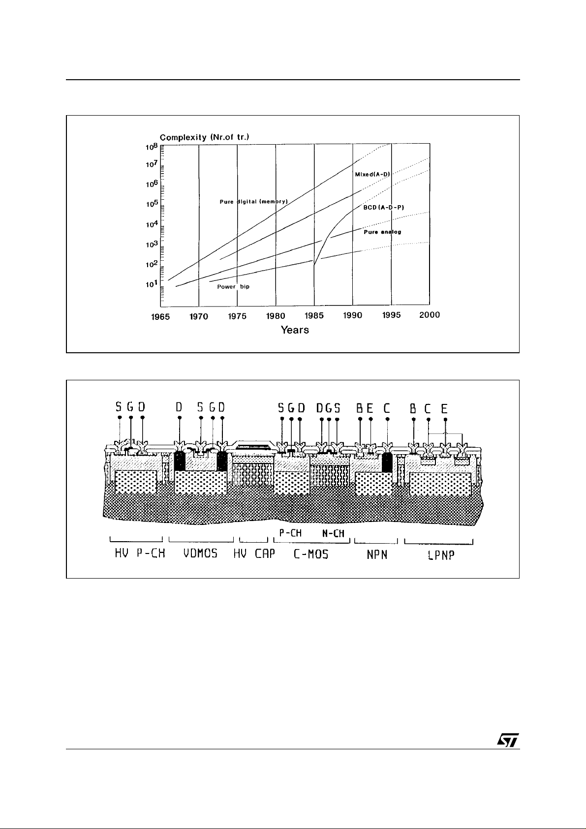
The technology architecture is bas ed on the vertical DMOS sil icon gate process that allows a chan nel
length of 1.5 micron ; using a junction isolation technique it has be en possible to mix on the same chip
Bipolar and CMOS transistors along with the DMOS power components (Fig. 2). Figure 1 shows how this
process brings a rapid increase in power IC complexity compared to conventional bipolar technology. In
the 70’s class B circuits and DC circuits allowed out put power in the range of 70W . By 1980, with the introduction of switching techniques in power ICs, output powers up to 200W were reached ; with BCD technology the output power increased up to 400W.
November 2003
1/52
Page 2
AN557 APPLICATION NO TE
Figure 1. BCD process and increase in power ICs complexity.
Figure 2. Cross Section of the BCD Mixed Technology.
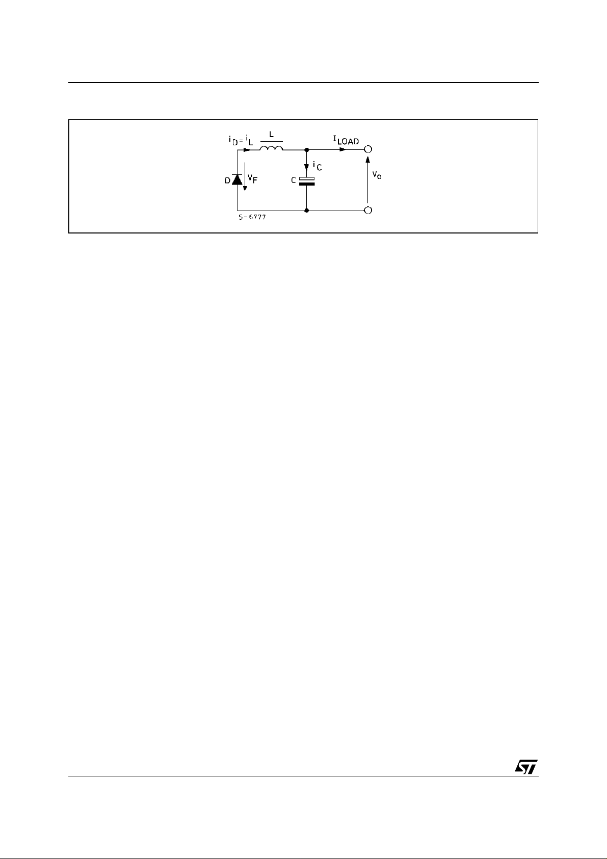
THE STEP-DOWN CONFIGURATION
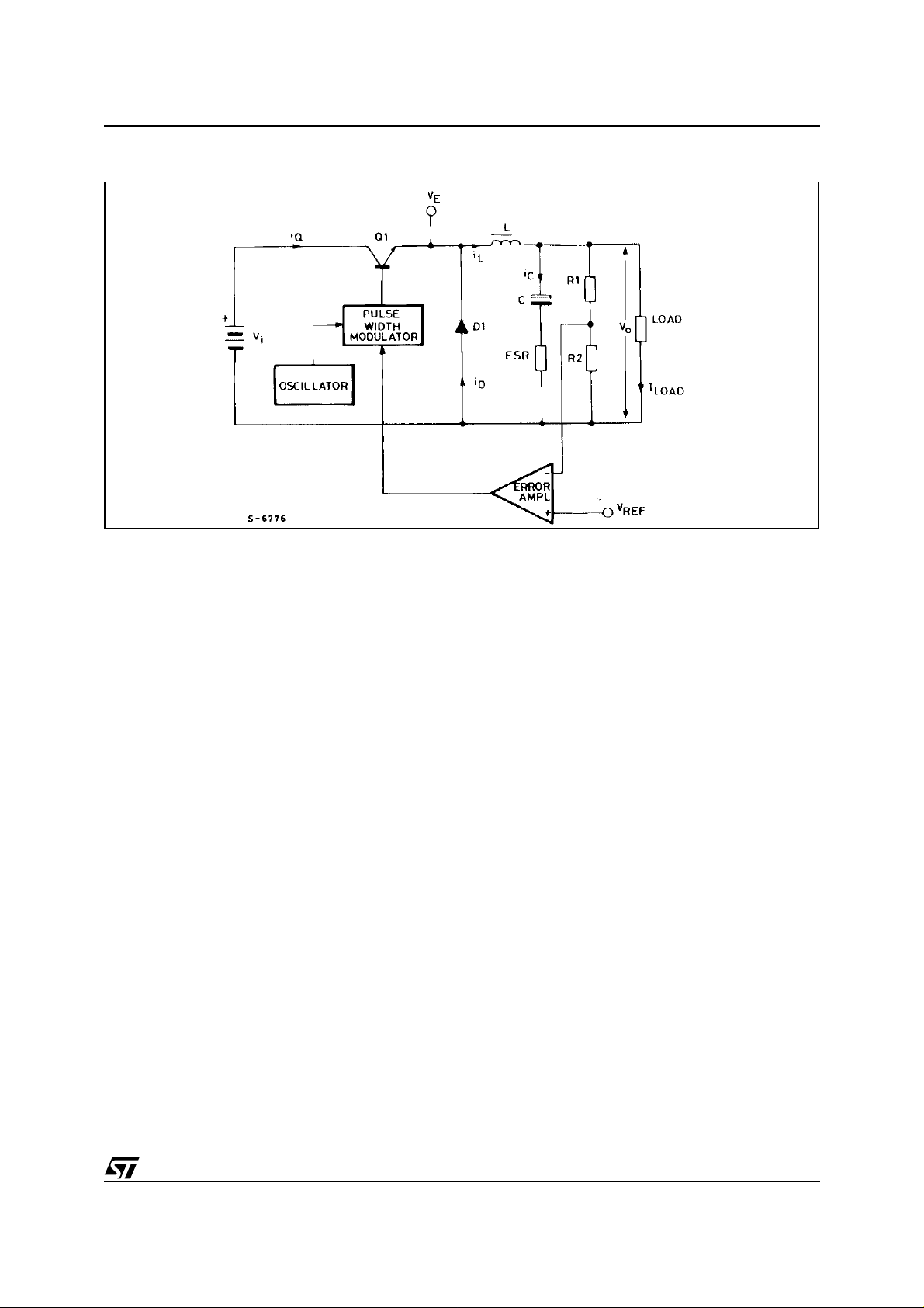
Fig. 3 shows the simp lified block di agram of the c i rcuit realizin g the s t ep-down c onfiguration. T his circuit
operates as follows : Q1 acts as a switch at the frequency f and the ON and OFF ti mes are suitably c ontrolled by the pulse width modulator circuit. When Q1 is saturated, energy is absorbed from the input which
is transferred to the output through L. The emitter voltage of Q1, V
, is Vi-Vsat when Q is ON and -VF (with
E
VF the forward voltage across the D dio de as indicated) when Q1 is OFF. During t his sec ond phase the
current circulates again through L and D. Consequently a rectangular shaped voltage appears on the emitter of Q1 and this is then filtered by the L-C-D network and converted into a continuous mean value across
the capacitor C and therefore across the load. The current through L consists of a continuous component,
I
, and a triangular-shaped component super-imposed on it, ∆IL, due to the voltage across L.
LOAD
2/52
Page 3
AN557 APPLICATION NOTE
Figure 3. The Basic Step-down Switching Regulator Configuration
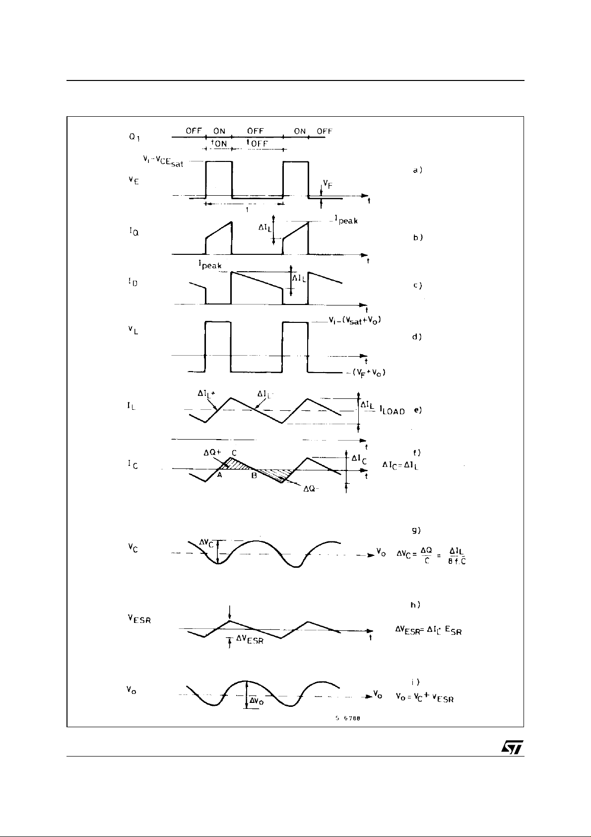
Fig. 4 shows the behaviour of the most significant waveforms, in different points of the circuit, which help
to understand better the operation of the power section of the switching regulator. For the sake of simplicity, the series resistance of the coil has been neglected. Fig. 2a shows the behaviour of the emitter voltage
(which is practically the voltage across the recirculation diode), where the power saturation and the forward VF drop across the diode era taken into account.
The ON and OFF times are established by the following expression :
T
ON
------------------------------- -
V
ViV
o
–()
sat
⋅=
T
+
ONTOFF
Fig. 4b shows the current across the switching tran sistor. The current shape is t rapezoida l and t he operation is in continuous mode . At this stage, the phenom ena due to the c atch diode, that we consider as
dynamically ideal, are neglected. Fig. 4c shows the current circulating in the recirculation diode. The sum
of the currents circulating in the power and in th e diode is the current circul ating in the c oil as s hown in
Fig. 4e. In balanced conditions the ∆
decrease occurring during T
OFF
+
current increase occ uring du ring TON has to be equal to the ∆ I
IL
L
. The mean value of IL corresponds to the charge current. The current rip-
ple is given by the following formula :
+
I
∆ I
L
It is a good rule to respect to I
-
∆
== =
L
oMIN
iVsat
----------------------------------------
≥ IL/2 relationship, that implies go od operation in co ntinuous mode.
–()V
V
–
o
L
T
ON
VoVF+
------------------- -
L
T
OFF
When this is not done, the regulator starts operating in discontinuous mode. This operation is still safe but
variations of the switching frequency may occur and the output regulation decreases.
Fig. 4d shows the behaviour of t he voltage ac ross coil L. In b alanced conditions, the mean value of the
voltage across the coil is zero. Fig. 4f shows the current flowing through the capacitor, which is the difference between I
In balanced conditions, the m ean current is equ al to zero, and ∆I
and I
L
LOAD
.
= ∆IL. The current IC through the ca-
C
pacitor gives rise to the voltage ripple.
This ripple consists of two components : a capacitive component, ∆V
, and a resistive component, ∆V
C
ESR
due to the ESR equivalent series resistance of the capacitor. Fig. 4g shows the capacitive component ∆V
of the voltage ripple, which i s t he i nteg ral of a triangular-shaped curren t as a function of time . Moreo ve r,
it should be observed that v
of charge ∆Q
+
supplied to the capacitor is given by the area enclosed by the ABC triangle in Fig. 4f :
(t) is in quadrature with iC(t) and therefore with the voltage V
C
. The quantity
ESR
–
,
C
3/52
Page 4
AN557 APPLICATION NO TE
Figure 4. Principal Circuit Waveforms of the figure 1 Circuit.
4/52
Page 5

Which therefore gives:
Q∆
∆
V
C
1
-- -
2
Q
----
C
AN557 APPLICATION NOTE
∆
I
T
L
------- -
---
⋅⋅=
2
2
∆
I
L
--------==
8fc
Fig. 4h shows the voltage ripple V
V
(t) = iC (t) × ESR. Fi g. 4i sh ows t he o vera ll ripple Vo, which is t he sum of the two pre vious com po-
ESR
due to the resistive component of the capacitor. This component is
ESR
nents. As the frequency increases (> 20kHz), which is required to reduce both the cost and the sizes of L
and C, the VESR component becomes dominant. Often it is necessary to use capacitors with greater capacitance (or more capacitors connected in parallel to limit the value of ESR within the required level.
We will now examine the stepdown configuration in more detail, referring to fig. 1 and taking the be-haviour
shown in Fig. 4 into account.
Starting from the initial conditions, where Q = ON, v
= Vo and iL = iD = 0, using Kirckoff second principle
C
we may write the following expression:
V
= vL + vC (V
i
is neglected against Vi).
sat
d
IL
i
------- -
L
dt
v
+ L
C
V
(1)
d
IL
+⋅==
------- - V
dt
o
which gives :
d
------- -
dt
V
IL
–()
iVo
---------------------- -=
L
(2)
The current through the inductance is given by :
ViVo–()
I
---------------------- -=
L
(3)
L
When Vi, Vo, and L are constant, IL varies linearly with t. Therefore, it follows that :
V
+
∆
I
L
–()T
iVo
---------------------------------- -=
L
ON
(4)
When Q is OFF the current through the coil has reached its maximum value, Ipeak and because it cannot
very instantaneously, the voltage across the ased to allow the recirculation of the current through the load.
When Q switches OFF, the following situation is present:
vC(t) = Vo, iL (t) = iD (t) = I
peak
And the equation associated to the following loop may be written :
d
IL
------- -
where : vC = V
V
L
++ 0=
F
o
dI
L
------- -
dt
dt
V
------------------------ -–=
v
FVo
C
(5)
+()
(6)
L
It follows therefore that :
+
V
FVo
t()
------------------- -
T
t–=
(7)
5/52
i
L
Page 6

AN557 APPLICATION NO TE
The negative sign may be interpretated with the fact that the current is now decreasing. Assuming that VF
may be neglected against V
therefore :
But, because ∆I
L
+
= ∆I
, during the OFF time the following behaviour occurs :
o
V
o
------
t=
V
------
L
ON
(8)
L
o
T
(9)
OFF
V
oTOFF
---------------------=
L
–
if follows that :
L
I
L
+
I
∆
=
L
–()T
V
iVo
---------------------------------- -
L
which allows us to calculate V
:
o
T
ON
V
------------------------- -
==
V
o
i
TONT
OFF
V
where T is the switching period.
Expression (10) links the output voltage V
to the input voltage Vi and to the duty cycle. The relat ion -sh i p
o
between the currents is the following :
T
ON
---------- -
I
iDCIoDC
⋅=
T
EFFICIENCY
The system efficiency is expressed by the following formula :
P
o
------
100⋅=
P
i
where Po = VoIo (with Io = I
system. P
is g ive n by Po, plus all t he other syst em losses. Th e expression of the effic iency becomes th ere-
i
η %
) is the output power to the load and Pi is the input power absorbed by the
LOAD
fore the following :
P
---------------------------------------------------------------------------------=
η
PoP
+ ++++
satPDPLPqpsw
o
T
ON
-----------
i
T
(11)
(10)
(12)
DC LOSSES
Psat :saturation losses of the power transistor Q. These losses increase as Vi decreases.
T
ON
P
ON
T
V
o
------=
V
i
is the power transistor saturation at current Io.
sat
T
where and V
P
---------- -
: losses due to the recirculatio n diode . These loss es incr ease as Vi increases, as in this case the ON
D
sat
V
satIo
---------- -
T
+⋅=
V
satIo
V
------
V
o
i
(13)
time of the diode is greater.
6/52
ViVo–
VFI
----------------- -
o
V
i
P
==
D
V
1
FIo
V
o
(14)
------–
V
i
Page 7

where VF is the forward voltage of the recirculation diode at current Io.
P
: losses due to the series resistance RS of the coil
L
AN557 APPLICATION NOTE
PL = RS I
o
2
(15)
Pq: losses due to the stand-by current and to the power driving current:
Pq = Vi Iq, (16)
in which Iq is the operat ing supply current at the operating swi tchin g frequency. Iq includes the oscillator
current.
SWITCHING LOSSES
P
: switching losses of the power transistor :
sw
trtf+
------------ -
=
P
sw
ViI
o
2T
The switching losses of the recirculation diode are neglected (which are anyway negligible) as it is assumed that diode is used with recovery time much smaller than the rise time of the power transistor.
We can neglect losses in the coil (it is assum ed that ∆ IL is very small comp ared to I
) and in the output
o
capacitor, which is assumed to show a low ESR.
Calculation of the inductance value, L
Calculation T
ON
and T
through (4) and (9) respectively it follows that :
OFF
T
ON
+
I
∆ L⋅
L
----------------- -= T
V
–
iVo
OFF
∆ L⋅
--------------- -=
-
I
L
V
o
But because :
+
T
ON
+ T
= T and ∆I
OFF
L
–
= ∆I
= ∆IL, it follows tha t :
L
T
ON
IL∆ L⋅
----------------- –
V
iVo
I
∆ L⋅
L
--------------- -+ T==
V
o
(17)
Calculating L, the previous relation becomes :
V
–()V
V
i
o
------------------------------
L
V
o
I
∆
i
L
T=
(18)
Fixing the current ripple in the coil required by the design (for instance 30% of Io), and introducing the frequency instead of the period, it follows that :
V
–()V
L
iVo
-------------------------------- -=
V
0.3 Iof⋅⋅⋅
i
o
where L is in Henry and f in Hz Vi × 0.3 × Io × f
Calculation of the output capacitor C
From the output node in fig. 3 it may be seen that the current through the output capacitor is given by:
ic (t) = iL (t) – I
o
7/52
Page 8
AN557 APPLICATION NO TE
Figure 5. Equivalent Circuit Showing Recirculation when Q1 is Turned Off.
From the behaviour shown in Fig. 4 it may be calculated that the charge curren t of the output capacitor,
within a period, is ∆I
but, remembering expression (4) :
therefore equation (19) becomes :
Finally, calculating C it follows that :
where :
L is in Henrys
C is in Farads
f is in Hz
Finally, the following expression should be true :
It may happen that to satisfy relation (21) a capacitance value much great er than the value calculated
through (20) must be used.
/4, which is supplied for a time T/2. It follows therefore that :
L
∆
------- -
VC∆
4C
V
+
∆
I
L
–()T
i
---------------------------------- -= T
∆
V
I
L
V
L
C
T
---
2
o
ON
V
----------------------------- -=
I
T∆
L
----------- -
8C
and
–()V
iVo
IL∆
--------===
8fc
ON
o
(19)
V
------
V
o
T=
i
8 Vif2LC
V
–()V
C
ESR
------------------------------------- -=
8 Vi VC f∆
max
iVo
∆
---------------------=
V
Cmax
∆
o
2
L
I
L
(20)
(21)
TRANSIENT RESPONSE
Sudden variations of the load current give rise to overvoltages an d und ervo ltages on th e output v oltage.
Since i
= C (dvc/dt) (22), where dvc = ∆Vo, the instantaneous variation of the load current ∆Io is supplied
c
during the transient by the output capacitor. During the transient, also current through the coil tends to
change its value. Moreover, the following is true :
di
L
------- -
=
v
L
(23)
L
dt
where diL = ∆Io
v
= Vi – Vo for a load increase
L
= Vo for a load decrease
v
L
8/52
Page 9
Calculating dt from (22) and (23) and equalizing, it follows that :
di
------- -
L
dt
dv
L
=
C
----------
C
i
C
AN557 APPLICATION NOTE
Calculating dv
and equalizing it to ∆Vo, it follows that :
C
V
∆
o
V
∆
o
LI
---------------------------=
CV
LI
-------------=
C V
∆
iVo
∆
2
o
–()
2
o
o
(24) for + ∆Io
(25) for -
∆
Io
From these two expressions the dependence of overshoots and undershoots on the L and C values may
be observed. To minimize ∆V
it is therefore necessary to reduce the inductance value L and to increase
o
the capacitance value C. Should other auxiliary functions be required in the circuit like reset or crowbar
protections and very variable loads may be p resent, it is worthwhile to t ake special care for minimi zing
these overshoots, which could cause spurious operation of the crowbar, and the under-shoot, which could
trigger the reset function.
DEVICE DESCRIPTION
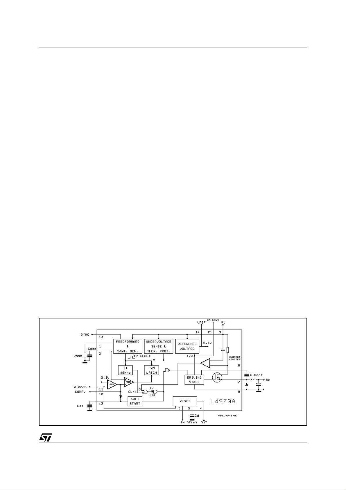
For a better understanding of how the dev ice f unc tions , a description will be given of the prin ciple blocks
that compose the device. The block diagram of the device is shown in fig.6
POWE R SU PPLY
The device contains a stabil ized regulator (Vstart = 12V ) that provides powe r to the a nalogic and digit al
control blocks as well as the section of the bootstrap. The Vstart voltage also powers the bl ocks that operates the internal reference voltage of 5.1V, with a precision of ±2%, necessary for the feedback.
OSCILLATOR, SYNC. AND VOLTAGE FEED-FORWARD FUNCTIONS
The oscillator block generates a sawtooh wave signal that sets the switching frequency of the system. This
signal, compared with the output voltage of the error amplifier, generates the PWM signal that will then
sent to the power output stag e. The oscillator also c ontains the voltage feedforward f unction that, be ing
completely integrated, does not require additional external components to function. The VFF function operates with supply voltages from 15V to 45V. The ∆V/∆t of the sawtooh is directly proportional to the supply
voltage Vi.
As Vi increases, the conduction time (ton) of the power transistor decreases in such way as to provide to
the coil, and therefore to the load, the product Volt x Sec constant.
Figure 6. Block Diagram of the 10A Monolithic Regulator L4970A.
9/52
Page 10
AN557 APPLICATION NO TE
Figure 7. Volta ge Feeforward Wa veform.
V2
V7
D93IN006
Vi=30V
Vi=15V
Vc
t
Vi=30V
Vi=15V
t
Fig. 7 shows the duty-cycle varies as a result of the changes in slope of the ramp with the input voltage
Vi. The output of the error amplifier shou ld not chang e to maintain the out put voltage i n regulation. This
function allows for the increas e of s peed in response to the rapid ch ange o f the supply voltage and for a
greatly reduced ouput ripple at the mains frequency.
In fact, the slope of the ramp is modulated by the ripple, generally present in the order of several volts on
the input of the regulator, particularly when the solution with a mains transformer is used.
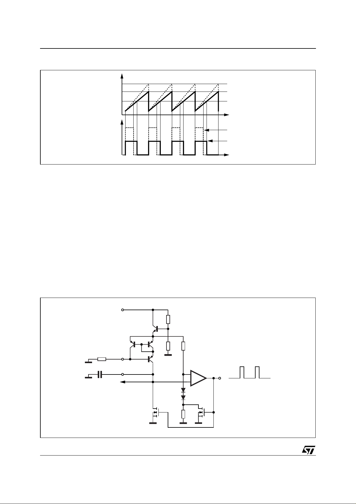
Fig. 8 shows the simplified electrical diagram of the oscillator.
A resistor, connected between the Rosc pin and GND, sets the current that is internally reflected in the pin
Cosc, in order to charge the external capacitor to which it is connected. The voltage to the Rosc pin is not
fixed, but is tied to the instantaneous value of Vi; this is needed t o achieve th e feedforward voltage function, in which the slope of the ramp is directly proportional t o the supply voltage. A comparator senses the
voltage at the Cosc capacitor. Wh en the voltage reaches the val ue present at the inverting input o f the
comparator, the output from the comparator goes high and is sent to the two transistors Q1 and Q2. Q1
is responsible for discharging the external Cosc capacitor with a current of approx. 20mA, while Q2 imposes at the inverted input of the comparator a voltage of 2Vbe (approx. 1.3V) that is the low-threshold of
the ramp. Some useful formulas for calculating the various parameters of the oscillator block are:
Figure 8. Osc illator Circuit.
Rosc
Cosc
PWM
COMP.
10/52
Vi
2R
13 2RR
Q1
-
+
Q2
R
CLOCK
D93IN007
Page 11

AN557 APPLICATION NOTE
1) Oscillator charge current:
Vi9V
–
I
CHARGE
-------------------------=
2) Oscillator discharge current:
3) Peak voltage ramp:
V
th H–
This formula is obtained in the following way: indicating with Ve the voltage of the emitter of the NPN transistor connected to Vcc, and V- the voltage at the inverted input of the comparator, one has:
V
V
V
------------------------- -
by substituting (a) into (b), one obtains:
V
i
---- - V
–
3
------------------------------- --------------- 2V
V
be
–
3
be
R
osc
I
= 20mA
DISCH
Vi9V
–
------------------------ - 2V
Rosc
V
i
–=
---- - V
e
3
2V
–
e
be
3R
2V
be
+=–
(For 15V < Vi < 45V)
be
+=
be
(a)
be
R⋅
+=–
be
2V
(b)
be
V
9V
–
i
be
------------------------- 2V
+=
9
be
4) Valley voltage ramp:
V
= 2V
th-L
be
5) Switching frequency:
SW
------------------------- -=
R
oscCosc
f
9
It should be noted that formula (5) does not take into account the discharge time of Cosc which cannot be
neglected when one is working at frequencies equ al or highe r than 20 0KHz. The d ischarge tim e is also
tied to the value of Cosc itsel f.
Analitycally one has:
6)
T
DISCH
V
th H–
-------------------------------------- -
–
20 mA
V
th L–
C
⋅=
osc
from which is obta ined the mor e clo se ly ap p ro x im a te ex pr e ss io n o f the o s c illat o r fr equency:
7)
f
SW
---------------------------------------- -----------------=
R
oscCosc
----------------------------- - T
1
⋅
+
9
DISCH
During the discharge time of Cosc, a clock pulse is generated internally that is made sub sequent ly available on the Sync. pin and that can be used to synchronize other regulators. (3 devices of the same family
maximum). The Sync. pulse generated has a typical range of 4.5V and the current availabi lity is 4.5mA.
In general, it is better that the Sync pulse is at least 300-400ns in order to be able to synchronize a range
of existing regulators; to obtain this result, values of suggested capacitors, in different test circuits, have
11/52
Page 12
AN557 APPLICATION NO TE
been selected. The typical duration of th e synchronizing pu lse with the suggest ed values of C
osc
are as
follo ws :
L497X Family (MULTIWATT PACKAGE)
C
(nf) - R
osc
L497X Family (POWERDIP PACKAGE)
C
(nf) - R
osc
= 16KΩ
osc
0.68 140
1230
1.2 270
1.5 330
2.2 450
3.3 680
4.7 1100
= 30KΩ
osc
1.2 230
1.5 280
2.2 420
3.3 600
4.7 900
Sync (ns)
Sync (ns)
Obviously, synchronize pulses of eccessive duration can greatly reduce the max duty-cycle and produce
distortions in the sawtooth of the synchronized regulator working as slave.
P.W.M.
Comparing the sawtooth signal generated by the oscillator and the output of the error amplifier, generates
the PWM signal which is sent to the driver of the output power stage. The PWM signal, in the path towards
the output stage, also encounters a latch block to prevent other pulses from being sent at same period to
the output, possibly damaging the power stage. In the PWM bl ock, a dut y-cycle limiter has al so been introduced. Such a limiter is obtained by taking advantage of the synchronizing pulse generated, the power
output stage is inhibited. Even if the error amplifier gives a large signal to the peak of the ramp, the power
stage will not b e able to op er ate in DC , but w ill be s wit ched of f at ea ch clock puls e. The max . obt ainable
duty-cycle is higher than 90%; this, however depends on the working frequency and the value of Cosc.
Using the formulas 6) and 7) a precise calculation can be done.
SOFT START
The Soft Start function is essential for a correct startup of the device and for an output voltage that, at the
switch on, increases in a monotonous mode without dangerous output overvoltages and without overstress for the power stage.
Soft Start operates at the startup of the system and after an intervention of the th ermal prot ection. Fig. 9
shows the simplified diagram of the startup functions. The function is carried out by means of an external
capacitor connected to the Soft Start pin, which is charged with a constant current of about 100µA to a
value of around 7V. During the charging time, the output of the error transcon-ductance amplifier, because
of Q1, is forced to increase at the same rising edge time of the external softstart capacitor Css.
12/52
Page 13
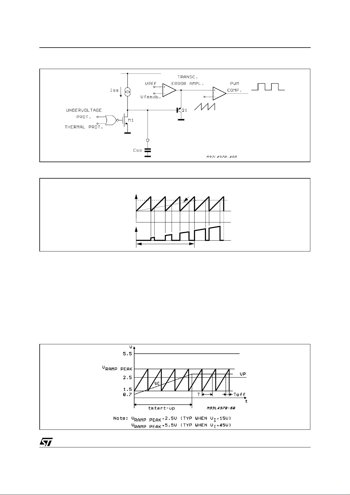
Figure 9. Soft Start Circuit.
Figure 10. Soft Start Waveforms.
Vc
AN557 APPLICATION NOTE
CLAMPED
ERROR AMPLIFIER
OUTPUT
t
OUTPUT
CURRENT
SOFT START TIME
D93IN011
t
The PWM signal begins to be generated as soon as the output voltage of the error amplifier crosses the
ramp; at this point the output stage begins to commutate, slowly increasing its ON time (see fig. 10).
The charge of the Css capacitor, as already mentioned, begins each time the device is supplied with power and after which an anomalou s condition is creat ed, as the intervent ion of thermal prot ection or of the
undervoltage lockout.
CALCULATING THE DUTY-CYCLE AND SOFT-START TIME
Let us suppose that the discharge tim e o f the osc illator capac itor, Cos c, is neglected. This is an approx.
valid for switching frequencies up to 200KHz. Let us indicate with Vr the output voltage of the error amplifier, and with Vc the voltage of the oscillator ramp.
Figure 11. Soft Sart Time Waveform.
13/52
Page 14

AN557 APPLICATION NO TE
The PWM comparator block commutates when Vr = Vc. Therefore:
i
9
t⋅
9V
–()⋅⋅
V
9V
–
i
------------------------ -
be
be
9T⋅
t⋅== =
8)
from which is obtained
9)
V
r
V
t
V
pp
--------- -
c
T
Vr T V
------------------------------------------------ -=
The time t obtained from this equation is equal to the ON time of the power transistor. The corresponding
duty-cycle is given by:
10)
Vr T V
t
on
-------
D
------------------------------------------------ -
T
9T
9V
–()⋅⋅
i
be
VrVi9V
--------------------------------------- -
–()⋅
be
9
V
o
------== = =
V
i
Consequently, after leaving the discharged capacitor of Soft Start, the output of the regulator will reach its
value when the voltage across the Css capacitor, charged w ith constant current, has reached the value
Vr - 0.5V.
The time necessary in order that the output rises from zero to the nominal value is given by:
Vr0.5V–()
11)
in which C
is the Soft Start capacitor and Iss the Soft Start current. Considering Soft Start time as tss,
ss
t
start up–
C
ss
---------------------------- -
⋅=
I
ss
the required time for the Soft Start capacitor to change itself approx from (2Vbe - 0.5V) = (1.2V - 0.5V) to
Vr - 0.5V, is:
Vr1.2V–()
12)
t
ss
C
ss
---------------------------- -
⋅=
I
ss
By taking Vr from (10):
13)
V
o
------
V
r
V
i
9
------------------------ -
⋅=
9V
–
V
i
be
and substituting it in (12), we obtain:
14)
o
---------
t
=
ss
------
I
V
ss
i
9
------------------------ - 1.2V–⋅
9V
–
V
i
be
V
C
ss
UNDERVOLTAGE LOCKOUT
The device contains the protection block of under-voltage lockout which keeps the power stage turned-off
as long as the supply voltage does not reach at least 12V. At this point the device starts up with Soft Start.
The function of undervoltage is also provided with an hysteresis of 1V to make it better immune to the ripple present on the supply voltage.
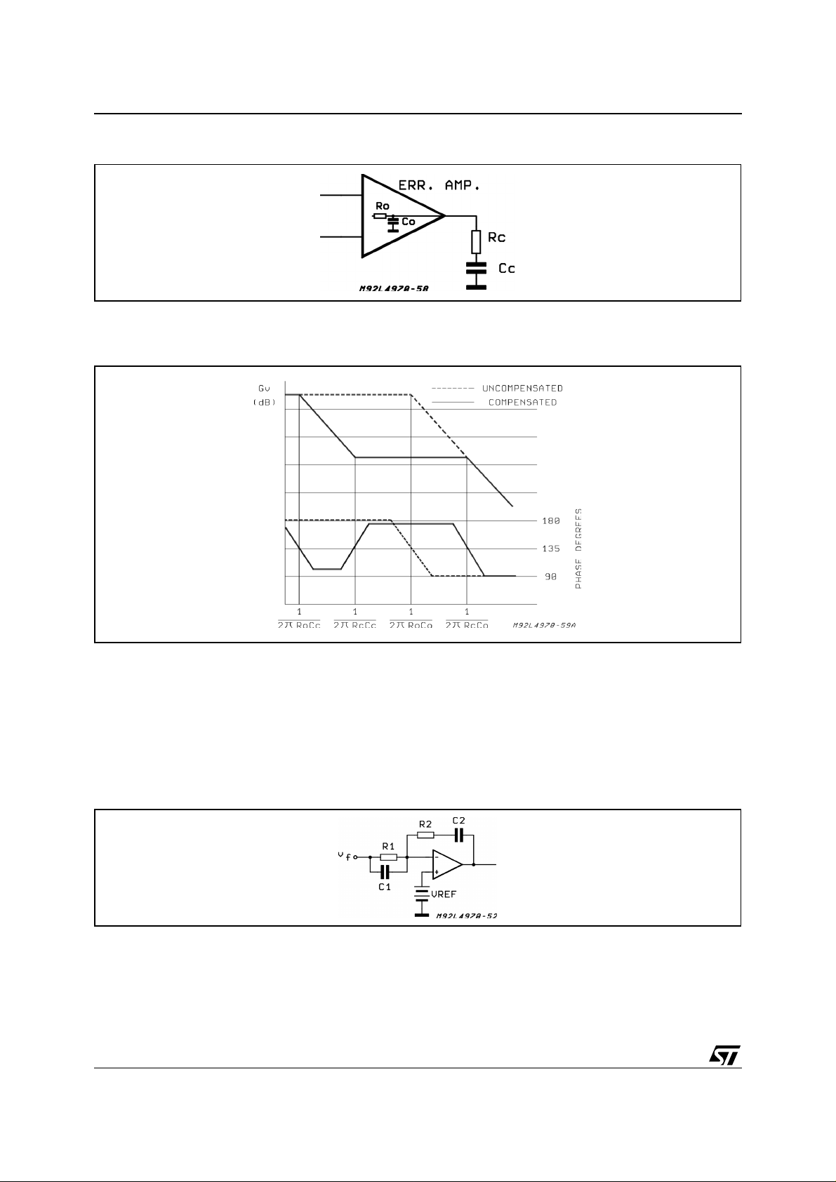
ERROR AMPLIFIER
The error amplifier is a transconductance type and deliver an output current proportional to the voltage inbalance of the two inputs . The s i mplified diagram is presented in f i g 12. Th e pri ncipal characteristics of t hi s
uncompensated operational ampl ifier are the following: Gm = 4mA/V, Ro = 2.5Mohm, Avo = 80dB, Isourcesink = 200
µ
A, Input Bias Current = 0.3µA. The frequency response of the op. amp. is given in fig. 13.
Ignoring the high frequency response and hypothesizing that the second pole is below the 0 dB axis in the
all the conditions of loop compensation, it is possible to make a first approximation with the equivalent circuit of fig. 14
14/52
Page 15
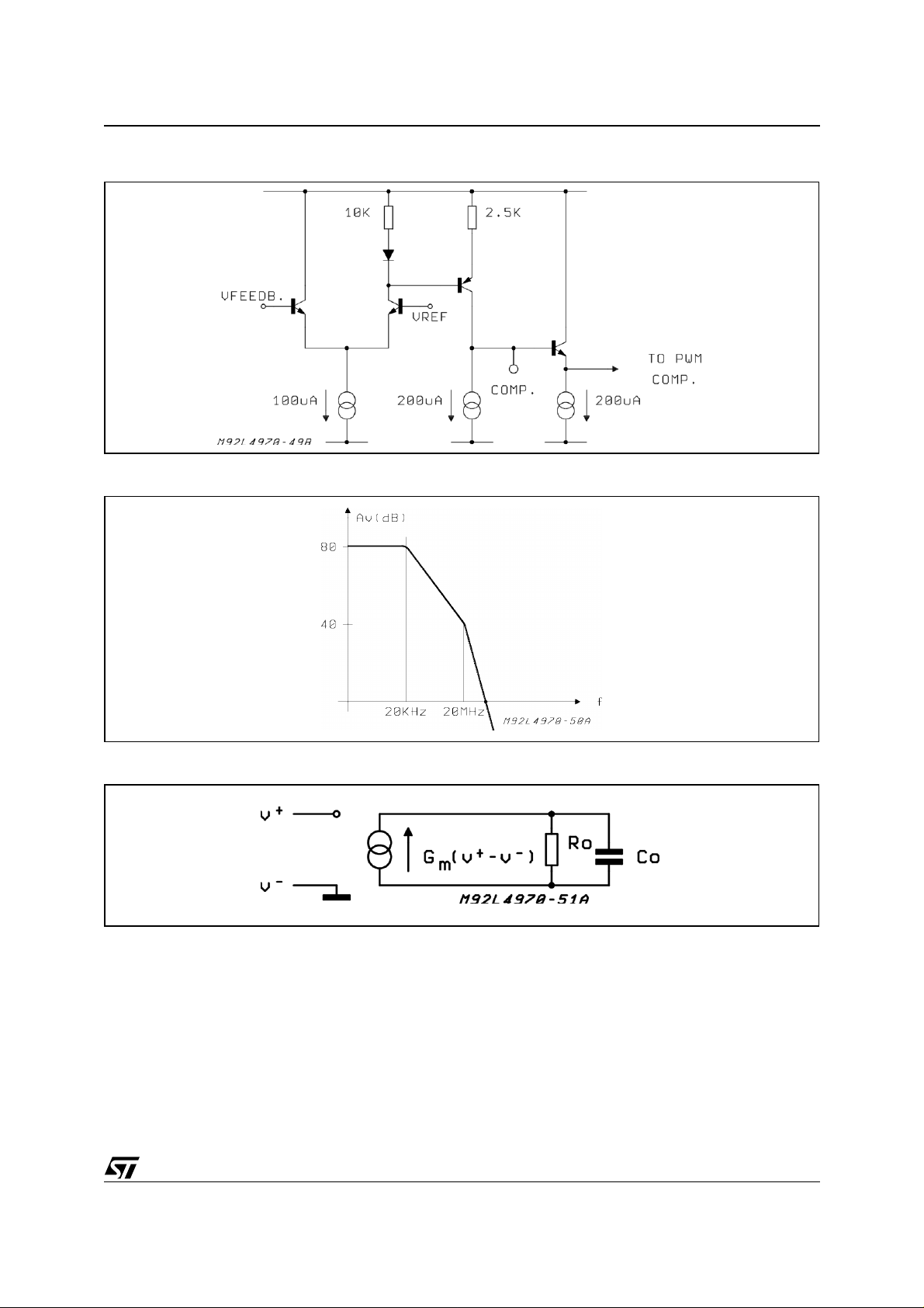
Figure 12. Error Amplifier Circuit.
Figure 13. Ope n l oop gai n ( error amplifier onl y )
AN557 APPLICATION NOTE
Figure 14. Error amplifier equivalent circuit.
In whic h :
15) where C
Av s() Gm
R
c
--------------------------- -
⋅=
1sRoC
+
o
= 3pF
o
The error amplifier can be easily compensated thanks to the high output impe dance (see fig. 14) The resulting transfer function is as in the following:
R
1sRcC
+()⋅
(16)
Av s() Gm
---------------------------------------------------------------------------------------------------------------------
⋅=
2
s
R
C
R
o
o
o
C
sRoCcRoCoRcC
c
c
c
++()1++
c
15/52
Page 16
AN557 APPLICATION NO TE
Figure 15. Compensation network of the error ampli fier
The Bode diagram is shown in fig.16.
Figure 16. Bode plot showing gain and phase of compens ated erro r ampl ifier
The compensation circuit introduces a pole at low frequency and a zero that is generally calculated to be
put in the proximity of the resonance frequency of the output LC filter.
The second pole at high frequency generally falls in a zone of no interest (for the system stability, one must
consider the zero introduced by ESR characteristic of the output capacitor. Not all the designers agree on
this solution).
If necessary, however, one c an turn t o m ore sophisticated compensation circuitry. An ex am ple is s hown
in fig. 17.
Figure 17. One pol e, tw o ze ro com p e nsation netw ork
Such a circuit introduces a pole at low-frequency and two zeros.
17
16/52
Z1
1
-----------------------------
2Π R1 C1
Z2
1
-----------------------------==
2Π R2 C2
Page 17

AN557 APPLICATION NOTE
It must be remembered, however, that because of the high out put impedance of t he error amplifier, a second pole is also present:
18)
P2
Gm
----------------- -=
2Π C1
We normally suggest a high value for R1 to reduce the value of the capacitor C1 and allocate the pole P2
at the highest possible frequency. The ess ential limitation t o the max v alue of R1 is the offset introduc ed
by the input bias current of the error amplifier. In the case of output voltage regulated higher than 5.1V, an
external divider should be introduced. It’s than possible to introduce a second zero using the following network:
Figure 18. Compensation network for output voltages higher than 5.1V
Two zeros and two poles are introduced:
19)
Z1
1
---------------------------
2Π R
o Cc
Z2
1
-----------------------------==
2Π R1 C1
Where
Rx
R1 R2⋅
--------------------- -=
R1 R2+
P1
1
---------------------------
2Π R
o Cc
P2
1
---------------------------- -==
2Π Rx C1
APPLICATION EXAMPLE
Consider the block diagram of fig. 19, represent ing the internal cont rol loop section, with the appl ication
values:
Fswitch = 200KHz, L = 100µH, C = 1000µF, Po = 50W, Vo = 5.1V, Io = 10A and Fo = 500Hz. G
loop
= PWM
× Filter
Figure 19. Block diagram used in stability calculation
17/52
Page 18

AN557 APPLICATION NO TE
Figure 20. Frequency behaviour of the circuit of fig. 19
The system requires that DC gain is maximum to achieve good accuracy and line rejection. Beyond this
a bandwidth of some KHz is usually required for a good load transient response. The error amplifier transfer function must guarantee the above constrainst. A compensation network that could be used is shown
in fig. 21.
As()
1sR1 C1+()1sR2C2+()
----------------------------------------------------------------------=
sR1 C1 (1+s
C1
--------- -
Gm
Figure 21. Compensation network.
Figure 22. Bod e pl ot of th e regulation loo p wi th t he com pensatio n net work of fig. 21.
dB
Gloop
ACSJ
40
PWM+FILTER
20
18/52
50Hz 500Hz 5Kz 50KHz
D93IN012
Page 19

AN557 APPLICATION NOTE
The criterium is to define Z1, Z2 close to the resonant pole of the output LC filter. The Gm/2ΠC1 pole must
be placed at a frequency at which open loop gain is below 0dB axis (fig. 22).
CURRENT LIMITING
A complete regulation system will be equipped with a good current limiter able to protect from load breaking and operator error controlls. The current limiting function is totally integrated and does not require any
external component. The output current is sensed by an internal low-value resistor, in series with the drain
of the DMOS vertical power transistor..
A precision current limitation of ± 10% relative at the peak current is guaranted. During overcurrent situation the pulse by pulse current limitation produce an output stage switching frequency reduction. The block
diagram of the current limiting is shown in fig. 23.
Figure 23. Current protection circuit.
In overcurrent situation the comparator send a signal at the flip-flop set input, an inhibit pulse is immediatly
generated from it and sended at the output stage switching off the power mos.
A reset pulse input in generated from an 40KHz internal oscillator.
After the first reset pulse the control loop will start to regulate the system an the output current will increase
following the principal oscillator frequency. If overcurrent condition is still present the current limiting will
be activate again.
This type of current limiting ensure a constant output current in overload or short circuit condition and allow
a good reliability at high frequency (500KHz) reduc ing the problems relative at the interna l signal delay
through the protection blocks. The inductor current in overload condition in shown in fig. 24.
Figure 24. Overload inductance current.
19/52
Page 20

AN557 APPLICATION NO TE
The 40K Hz i nte rnal o scil lato r is syn chro nized wit h t he p rincip al o ne . If t he syst em w ork with a osc illator
tracks the principal oscillator frequenc y. In t his w ay the s witching frequenc y w i ll not increase in overload
situation.
A particular care has to be taken in the inductor value in order to avoid problems during overload or short
circuit conditions. A critical situation is present with high switching frequency, (more than 200KHz) where
a small inductor value is used and with high capacitive load.
In order to return in nominal condition after a short circuit the inductor ripple at 40KHz with the nominal
output voltage and current has to be lower than the current limitation value.
Example
Let us consider L4970A, 10A. (the same approach can be used for all the family).
The inductor ripple current is given by the following formula:
V
–()V
⋅
I
∆
L
iVo
--------------------------------- -=
fsw L⋅⋅
V
i
where fsw = 40KHz ±10%
In order to get the maximum inductor ripple current, the previous formula becomes:
V
–()V
imaxVomax
---------------------------------------------------------------- -=
I
∆
L
V
imaxfswmin
The current limitation for L4970A will start to work at 13A. therefore:
I
lim minIonom
o
⋅
L⋅⋅
IL∆
--------+>
2
omax
where I
= 10A for L4970A.
onom
POWER FAIL-RESET CIRCUIT
The L4970A include a voltage sensing c ircuit that may be used to g enerate a power on power off re set
signal for a microprocessor system. The circuit senses the input supply voltage and the output generated
voltage and will generate the required reset signal only when both the sensed voltages have reached the
required value for correct system operation. The Reset signal is generated after a delay time programmable by an external capacitor on the delay pin. Fig 25 shows the circuit implementation of Reset circuit. The
supply v oltag e is s ens ed on a n ex ter nal pin, for pr ogra mmab ilit y of the th resh old, by a f irst com par ato r.
The second comparator ha s the ref erence t hreshold set at s lightly les s the ref . voltag e for t he regulation
circuit and the other input connected internally at the feedback point on the regulated voltage. When both
the supply voltage and the regulated voltage are in the c orrect range, t ransistor Q1 turns off and a llows
the current generator to charge th e delay capacitor discharges c ompletely before initialization of a new
Reset cycle. The output gate assures immediate take of reset signal without waiting for complete discharge of delay capacitor. Reset output is an open collector transistor capable of sinking 20mA at 200mV
voltage. Fig 26 shows reset waveforms.
20/52
Page 21

Figure 25. Power fail and reset circuit.
Figure 26. Reset and power fail and reset circuit.
Vi
RISING P.FAIL
THRESHOLD
TURN-ON
THRESHOLD
11V
FALLING P.FAIL
THRESHOLD
10V
AN557 APPLICATION NOTE
TURN-OFF THRESHOLD
t
Vo=5.1V
RISING RESET
THRESHOLD
OUTPUT RESET
DELAY RESET POWER FAIL TIME
Figure 27. Power stage circuit.
5V
4.9V
FALLING
RESET
THRESHOLD
tDR tDR
HISTERESIS
t
5.1V
100mV
t
t
D93IN013
21/52
Page 22

AN557 APPLICATION NO TE
POWE R STAGE
The simplified diagram of the output stage is shown in the fig. 27.
The power stage and the circuit connected with it are by far the m ost important and critical com ponents
when one wants to obtain good performance at high switching frequency.
The power transistor must have excellent characteristics from the point of view of both the switching speed
and the robustness.
The transistor DMOS, with its intrinsic characteristics of elevated speed, no second breakdown phenomenom and
easy dr iving proves to be particularly suitab le for this type of applic ation that no rmally works at high frequ ency.
For a properly driving of the DMOS gate it is necessary to use an external bootstrap capacitor. When the
voltage Vs is low the Cboot capacitor is charged through the internal diode D1, at the value of voltage
equal to that of Vstart, which is about 12V; the next step oversees that Q3 is turned off, Q2 is driven in
gate by Q1 so that Q1 can go in saturation, and its source can go up rise towards Vi.
Cboot maintains its charge and guarantees a voltage equal Vi+12V a t the gate of Q7, so t hat can enter
into region of low resistance.
At this point the diode D1 turns o n to be inversely polarized, disc onnecting the 12V sect ion from that of
the driving power stage.
When Q2 is ON the driven current of the power stage requires from the bootstrap capacitor a typical current of 400uA.
When Q2 is Off a curren t of 2.5mA is required to mantain Q2 in that state. This current however is not
delivered from the bootstrap capacitor, but rather from the internal regulator of 12V, while the output current flowing in the freewheeling diode. The circuit described is capable of obtaining commutation, rise and
fall time, a typical value of 50ns.
In principle, it would have been feasible to reduce furthermore the commutation time whithout any reliability problems.
This was not believed to be advantageous since it would not have been of any benefit if one thinks of the
trr time of the catch diode (with trise of 50ns also the Schottky diodes begin to show limitations) and of the
conseguent increase of different disturbances caused bt too higly elevated dI/dt. The following table
shows the main features of the DMOS transistor.
Figure 28. Gate-charge curve for the power
Table 1.
B
VDSS > 60V at ID = 1mA VGS = 0V
DS(ON) = 100mΩ at ID = 10A Tj = 25°CVGS = 10V
R
R
DS(ON) = 150mΩ at ID = 10A Tj = 150°CVGS = 10V
TH = 3V at ID = 1mA
V
22/52
Page 23

AN557 APPLICATION NOTE
THERMAL SHUTDOWN
The thermal protection intervenes when the junction temperature reaches 150°C; it intervenes directly on
the output stage turning it off quikly and in the meantime discharging the soft start capacitor.
The reference voltage and the oscillator will continue to work regularly.
The thermal shutdown has a hysteresis, after its intervention, it is ne cessary to wai t for t he junction tem-
perature to lower around 30°C before the device will begi n to work properly again.
The device restart to work by using the soft start function.
Table 2. High Current Switching Regulator ICs.
L497X FAMILY
Parameter
Max. Input Operating
Voltage
Output Voltage Range 5.1V (±2%) to 40V
Max. Output Current 10A 7A 5A 3.5A 2A 2A
Power Switch
at 25°C
R
DSON
Switching Mode Control
System
Max. Switching Freq. 500KHz 500KHz 500KHz 200KHz 200KHz 200KHz
Efficiency
V
= 35V
INPUT
V
= 5.1V
OUT
Current Limiting Constant Current
Soft Start Yes
Reset and Power Fail Yes
Synch Yes
Crowbar No
Package
Max. R
th j-case (pin)
R
th j-amb
L4970A L4977A L4975A L4974A L4972A
50V 50V 50V 50V 50V 50V
0.13Ω typ.
Continuous Mode, Direct Duty Cycle Control with Voltage Feed-Forward
10A
80%
at 200KHz
Multiwatt15
1°C/W
35°C/W
7A
80%
at 200KHz
Multiwatt15
1°C/W
35°C/W
5A
85%
at 200KHz
Multiwatt15
1°C/W
35°C/W
3.5A
85%
at 100KHz
Powerdip
16+2+2
12°C/W
60°C/W
2A
85%
at 100KHz
Powerdip
16+2+2
12°C/W
60°C/W
L4972AD
Surf. Mount.
2A
85%
at 100KHz
SO20L
6°C/W
80°C/W
APPLICATIONS
Even though the regulators of the L4970A family has been designed to work only in step down configuration we will see next how these regu lators can be u se in large range of applications. In sam e cases the
L4970A device will be u sed as an example for t he entire family assembled in Multiwatt pac kage and the
L4974A will be used for the types in powerdip package.
Anyway the suggested applications can be extended to any other device of the family by adjusting if necessary the external components using the given equation for the calculation.
Typical Application
The Fig. 29 shows the electrical diagram of the typical application, complete with all the auxiliary functions.
The same application suggested in the data sheet as test circuit and is the same used for the final dynamic
test. All our devices are 100% tested both in static and dynamic conditions.
Included in the dynamic t est a re obviousl y the ex terna l com ponents : the coil, c atch diode and ou tput c apacitor which have been defined for all regulators.
Shown below are the electrical diagram s of 5 dev ices th at compos e the f am ily of th is regulator c om plete
23/52
Page 24

AN557 APPLICATION NO TE
with the value of the external components and with the relative pcb layout.
Output voltages higher than 5.1V are possible using an output resistive divider. For Vo > 24V, for safety
reasons it must be avoided the zero load condit ion. In the app lication with high current, co nnecte d to the
output divider are added two other res istanc es that perm it th e separat ion of sens ing and f orcing, in suc h
way as to compensate the fall of voltage on the connecting cables between the output and the load.
Connecting directly the output to the feedback pin a 5.1V ±2% is obtained. The following table can be help
for a rapid calculation of a resistor divider to obtain some of the most standard output voltage.
Figure 29. L4970A Typical Application Circuit.
Figure 30. Test and Evaluation Board Circuit
TYPICAL PERFORMANCES (using evaluation board) :
n = 83% (V
V
o RIPPLE
Line regulation = 5mV (V
Load regulation = 15mV (I
= 35V ; Vo = V
i
; Io = 10A ; fSW = 200KHz)
REF
= 30mV (at 10A) with output filter capacitor ESR ≤ 60m Ω
= 15 to 50V)
i
= 2 to 10A)
o
For component values, refer to test circuit part list.
24/52
Page 25

AN557 APPLICATION NOTE
PARTS LIST
R1 = 30KΩ * C1, C2 = 3300µF 63VL EYF (ROE)
R2 = 10KΩ C3, C4, C5, C6 = 2.2µF
R3 = 15KΩ C7 = 390pF Film
R4 = 16KΩ C8 = 22nF MKT 1817 (ERO)
R5 = 22Ω 0,5W
R6 = 4K7 C9 = 2.2nF KP1830
R7 = 10Ω C10 = 220nF MKT
R8 = see tab. A C11 = 2.2nF MP1830
R9 = OPTION **C12, C13, C14 = 220µF 40VL EKR
R10 = 4K7 C15 = 1µF Film
R11 = 10Ω
D1 = MBR 1560CT (or 16A/60V or equivalent)
L1 = 40µH core 58071 MAGNETICS 27 TURNS Ø 1,3mm (AWG 16) COGEMA 949178
* 2 capacitors in parallel to increase input RMS current capability
** 3 capa c i tors in parall e l t o reduce total ou tput ESR
Table A
V0 R10 R8
12V 4.7KΩ 6.2KΩ
15V 4.7KΩ 9.1KΩ
18V 4.7KΩ 12KΩ
24V 4.7KΩ 18KΩ
Table B
SUGGESTED BOOTSTRAP CAPACITORS
Operating Frequency Bootstrap Cap.c10
f = 20KHz ≥680nF
f = 50KHz ≥470nF
f = 100KHz ≥330nF
f = 200KHz ≥220nF
f = 500KHz ≥100nF
25/52
Page 26
AN557 APPLICATION NO TE
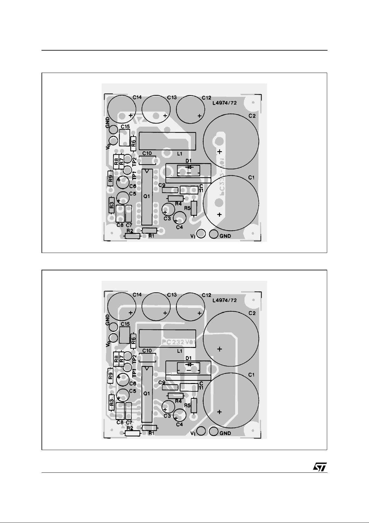
Figure 31. P.C. Board (co m po ne n t side) and Comp onents Lay out of t he C ir c ui t of Fig . 30.
Figure 32. P.C. Board (back side) and Components Layout of the Circuit of Fig. 30.
26/52
Page 27

AN557 APPLICATION NOTE
Figure 33. Test and Evaluation Board Circuit.
TYPICAL PERFORMANCES (using evaluation board) :
n = 83% (V
= 15 to 50V); Load regulation = 7mV (Io = 0.5 to 2A); for component values Refer to the fig. 32 (Part list).
(V
i
= 35V ; Vo = V
i
PARTS LIST
R1 = 30KΩ C3, C4, C5, C6 = 2.2µF 50V
R2 = 10KΩ C7 = 390pF Film
R3 = 15KΩ C8 = 22nF MKT 1837 (ERO)
R4 = 30KΩ C9 = 2.7nF KP1830 (ERO)
R5 = 22Ω C10 = 0.33µF Film
R6 = 4K7 C11 = 1nF
R7 = see tab. A **C12, C13, C14 = 100µF 40VL EKR (ROE)
R8 = OPTION C15 = 1µF Film
* C1, C2 = 1000µF 63V EYF (ROE) D1 = SB 560 (or equivalent)
L1 = 150µH core 58310 MAGNETICS 45 TURNS 0.91mm (AWG 16) COGEMA 949181
* 2 capacitors in parallel to increase input RMS current capability
** 3 capacit ors in parallel t o reduce tot al out put ESR
Table A
V0 R10 R8
12V 4.7KΩ 6.2KΩ
15V 4.7KΩ 9.1KΩ
18V 4.7KΩ 12KΩ
24V 4.7KΩ 18KΩ
Note: In th e T est and App l ication Circ ui t for L4972D are not mounted C2, C14 and R8.
; Io = 2A ; fsw = 100KHz); V
REF
o RIPPLE
= 30mV (at 1A); Line regulation = 12mV
Table B - SUGGESTED BOOTSTRAP CAPACITORS
Operating Frequency Bootstrap Cap.c10
f = 20KHz ≥680nF
f = 50KHz ≥470nF
f = 100KHz ≥330nF
f = 200KHz ≥220nF
f = 500KHz ≥100nF
27/52
Page 28

AN557 APPLICATION NO TE
Figure 34. Com p onent Lay ou t of f ig . 33. Eval uation Boar d
Figure 35. Board and Component Layout of the ciruit of fig. 33.
28/52
Page 29

AN557 APPLICATION NOTE
Figure 36. Test and Evaluation Board Circuit.
TYPICAL PERFORMANCES (using evaluation board) :
n = 83% (V
12mV (V
= 35V ; Vo = V
i
= 15 to 50V); Load regulation = 7mV (Io = 0.5 to 3.5A); for component values Refer to t he fig. 35
i
(Part list).
PART S L I ST
R1 = 30KΩ C3, C4, C5, C6 = 2.2µF 50V
R2 = 10KΩ C7 = 390pF Film
R3 = 15KΩ C8 = 22nF MKT 1837 (ERO)
R4 = 30KΩ C9 = 2.7nF KP1830 (ERO)
R5 = 22Ω C10 = 0.33µF Film
R6 = 4K7 C11 = 1nF
R7 = see tab. A **C12, C13, C14 = 100µF 40VL EKR (ROE)
R8 = OPTION C15 = 1µF Film
* C1, C2 = 1000µF 63V EYF (ROE) D1 = SB 560 (or equivalent)
L1 = 150µH core 58310 MAGNETICS 45 TURNS 0.91mm (AWG 16) COGEMA 949181
* 2 capacitors in parallel to increase input RMS current capability
** 3 capacit ors in parallel t o reduce tot al out put ESR
Table A
V0 R10 R8
12V 4.7KΩ 6.2KΩ
15V 4.7KΩ 9.1KΩ
18V 4.7KΩ 12KΩ
24V 4.7KΩ 18KΩ
Note: In th e T est and App l ication Circ ui t for L4974D are not mounted C2, C14 and R8.
; Io = 3.5A ; fsw = 100KHz); V
REF
o RIPPLE
= 30mV (at 1A ); Line regulation =
Table B - SUGGESTED BOOTSTRAP CAPACITORS
Operating Frequency Bootstrap Cap.c10
f = 20KHz ≥680nF
f = 50KHz ≥470nF
f = 100KHz ≥330nF
f = 200KHz ≥220nF
f = 500KHz ≥100nF
29/52
Page 30
AN557 APPLICATION NO TE
Figure 37. Com p onent Lay ou t of f ig . 36. Eval uation Boar d
Figure 38. Board and Component Layout of the ciruit of fig. 36.
30/52
Page 31

AN557 APPLICATION NOTE
Figure 39. Test and Evaluation Board Circuit
TYPICAL PERFORMANCES (using evaluation board) :
n = 83% (V
= 35V ; Vo = V
i
capacitor ESR ≤ 60mΩ; Line regulation = 5mV (V
For component values, refer to test circuit part list.
PARTS LIST
R1 = 30KΩ R11 = 10Ω
R2 = 10KΩ * C1, C2 = 3300µF 63V
R3 = 15KΩ C3, C4, C5, C6 = 2.2µF
R4 = 16KΩ C7 = 390pF Film
R5 = 22Ω 0,5W C8 = 22nF MKT 1817 (ERO)
R6 = 4K7 C9 = 2.2nF KP1830
R7 = 10Ω C10 = 220nF MKT
R8 = see tab. A C11 = 2.2nF MP1830
R9 = OPTION **C12, C13, C14 = 220µF 40VL EKR
R10 = 4K7 C15 = 1µF Film
D1 = MBR 760CT (or 7.5A/60V or equivalent)
L1 = 80µH core 58930 MAGNETICS 47 TURNS Ø 1,13mm (AWG 76) COGEMA 949178
* 2 capacitors in parallel to increase input RMS current capability
** 3 capa c i tors in parall e l t o reduce total ou tput ESR
Table A
V0 R10 R8
12V 4.7KΩ 6.2KΩ
15V 4.7KΩ 9.1KΩ
18V 4.7KΩ 12KΩ
24V 4.7KΩ 18KΩ
Table B - SUGGESTED BOOTSTRAP CAPACITORS
Operating Frequency Bootstrap Cap.c10
f = 20KHz ≥680nF
f = 50KHz ≥470nF
f = 100KHz ≥330nF
f = 200KHz ≥220nF
f = 500KHz ≥100nF
; Io = 5A ; fSW = 200KHz); V
REF
= 15 to 50V); Load regulation = 15mV (Io = 2 to 5A);
i
EYF (ROE)
L
o RIPPLE
= 30mV (at 10A) with output filter
31/52
Page 32

AN557 APPLICATION NO TE
Figure 40. P.C. Board (co m po ne n t side) and Comp onents Lay out of t he C ir c ui t of Fig . 39.
Figure 41. P.C. Board (back side) and Components Layout of the Circuit of Fig. 39.
32/52
Page 33

AN557 APPLICATION NOTE
Figure 42. Test and Evaluation Board Circuit
TYPICAL PERFORMANCES (using evaluation board) :
n = 83% (V
= 35V ; Vo = V
i
pacitor ESR ≤ 60mΩ; Line regulation = 5mV (V
component values, refer to test circuit part list.
PART S L I ST
R1 = 30KΩ R11 = 10Ω
R2 = 10KΩ * C1, C2 = 3300µF 63V
R3 = 15KΩ C3, C4, C5, C6 = 2.2µF
R4 = 16KΩ C7 = 390pF Film
R5 = 22Ω 0,5W C8 = 22nF MKT 1817 (ERO)
R6 = 4K7 C9 = 2.2nF KP1830
R7 = 10Ω C10 = 220nF MKT
R8 = see tab. A C11 = 2.2nF MP1830
R9 = OPTION **C12, C13, C14 = 220µF 40VL EKR
R10 = 4K7 C15 = 1µF Film
D1 = MBR 1560CT (or 16A/60V or equivalent)
L1 = 40µH core 58071 MAGNETICS 27 TURNS Ø 1,3mm (AWG 16) COGEMA 949178
* 2 capacitors in parallel to increase input RMS current capability
** 3 capa c i tors in parall e l t o reduce total ou tput ESR
Table A
V0 R10 R8
12V 4.7KΩ 6.2KΩ
15V 4.7KΩ 9.1KΩ
18V 4.7KΩ 12KΩ
24V 4.7KΩ 18KΩ
Table B - SUGGESTED BOOTSTRAP CAPACITORS
Operating Frequency Bootstrap Cap.c10
f = 20KHz ≥680nF
f = 50KHz ≥470nF
f = 100KHz ≥330nF
f = 200KHz ≥220nF
f = 500KHz ≥100nF
; Io = 7A ; fSW = 200KHz); V
REF
= 15 to 50V); Load regulation = 15mV (Io = 2 to 7A); For
i
EYF (ROE)
L
o RIPPLE
= 30mV (at 7A ) with out put filter ca-
33/52
Page 34

AN557 APPLICATION NO TE
Figure 43. P.C. Board (co m po ne n t side) and Comp onents Lay out of t he C ir c ui t of Fig . 42.
Figure 44. P.C. Board (back side) and Components Layout of the Circuit of Fig. 42.
34/52
Page 35

AN557 APPLICATION NOTE
Resistors value for standard output voltages.
Vo
(V)
12 4.7 6.2
15 4.7 9.1
18 4.7 12
24 4.7 18
Rx
(kΩ)
Ry
(kΩ)
Rx corresponds to R9 for L4974A and L4972A Ry
corresponds to R10 for L4970A, L4977A and
L4975A
Rx corresponds to R7 for L4974A and L4972A Ry
corresponds to R8 for L4970A, L4977A and
L4975A
The suggested switching frequency, and used in
the dynamic tests, is 200KHz for t he Multiwatt
package (MW) and 100KHz for the powerdip plastic package (PDIP). The maximum switching frequency allowed is 500KHz.
For the types in plastic package (Powerdip), the
lower switching frequency suggested is on ly depended by the minor dissipating power of a plastic
package versus a "power package" becau se it is
well known that switching losses are directly proportional to the commutation frequency. Higher
switching frequencies are possible if limited output
current is required and the operating ambient temperature are lower than 7 0°C. Infact the os cillator
of the devices ass embled in dual in line is completely equivalent to Multiwatt
®
package.
The most important external components which
need a little more attention (because a properly dimensioning affects on the performance of t he application) are the input and output capacitors, the
freewheeling diode and the coil.
Figure 45. Oscillator waveform and sync. pulse
for V
= 35V
i
Figure 46. Oscillator waveform and sync. pulse
for V
= 15V
i
®
Figure 47. Os cillo s co pe ph ot og ra p h s ho wi ng
the short circuit output voltage and
current waveforms .
INPUT OUTPUT CAPACITORS
The output voltage ripple ∆Vo, essentially depends on the current ripple in the coil and the ESR
of the output capacitor at the switching frequency.
The capacitor that present a low ESR are capable
of supporting higher current ripples.
Today, the majorit y of the cons tructors of el ec -trolithic capaci tors offe r in their da ta book also a wide
range of "low ESR" types generally suggested for
switching power supply application. In our case
EKR and EKE series (ROE ) has been preferred.
Such a series capacitors are designed for applications at high frequency, 200KHz, and built to have
a low ESR in order of supporting high current ripple.
In order to minimize the effects caused by the ESR
of the capacitors on the output voltage ripple 3 capacitors of 220uF/40V (for high output current application) are connected in parallel.
35/52
Page 36

AN557 APPLICATION NO TE
It is necessary much attention also into the choice input capacitors. Also them be at low ESR, because
they must sustain high current ripples. Such current ripples in presents of an inadeguate ESR, would produce a heating of the capacitor itself (which could affect on the reliability of the component, since in general it is sensitive to temperature.
Therefore choosing input capacitor at low ESR is necessary for problems of reliability. In fact such capacitors, when used in applications that make use a mains transformer, must support quite elevated peak current for short periods a double the mains frequency and the same time be capable to deliver the
instantaneous peak of energy to the load at the switching frequency.
Some other considerations of a general nature can be done on low ESR capacitors. For example of equal
value and type (i.e.: 220µF - EKR), the ESR of the capacitor decreases at the increasing of its value voltage rating, just like its RMS current.
Still, two capacitors of the same va lue, connected in parallel, withstand an R MS current hig her then the
only one of double value, and with the same voltage rating.
When however, more capacitors are connected together in parallel, it is important to design with care the
layout of the printed circuit, in order to distribute as eventy as possible amongst between the different capacitors the total current ripple.
This is used to avoid dangerous current unbalances in the distribution of the total current between the various capacitors charging some more others, that could damage the reliability of the system.
Often it is very difficult to know exactly the RMS current flowing throught the capacitors. To know if the
operating condition is a "safe"operat ing condition or not, a mea surement of the pack age temperat ure of
the capacitor should be done.
The following table 3 and 4, included in the dat-abook of electrical Roederstain, shows the maximum RMS
current sustainable by the EKR and EKE capacitor versus the ambient temeperature and overtemperature
allowed on the capacitor package.
Table 3. Low-voltage electro lytic ca paci tors for sw itch-m od e power supplies with low im p edan ce
values, radial, polarized styles
Rated cap.
(µF)
EKR
100
220
470
100
220
470
100
220
470
100
220
470
Rated volt.
(V DC)
10
10
10
16
16
16
25
25
25
40
40
40
Dimensions
D x L (mm)
(nominal
dimen-
sions)
8.7 x 12.7
10 x 12.7
10 x 20
10 x 12.7
10 x 16
12.5 x 20
10 x 12.7
10 x 16
12.5 x 20
10 x 16
12.5 x 20
12.5 x 30
Dissipation
factor tan δ
(100Hz;
20°C) Lim.
Values
0.12
0.12
0.12
0.11
0.11
0.11
0.09
0.09
0.09
0.08
0.08
0.08
Impedance
Z (Ω)
(10KHz;
20°C)
(Lim. val-
ues)
0.85
0.39
0.20
0.60
0.32
0.16
0.5
0.25
0.13
0.4
0.17
0.09
Impedance
Z (Ω)
(10KHz;
20°C)
(Lim. val-
ues)
0.65
0.31
0.18
0.40
0.25
0.13
0.35
0.17
0.09
0.23
0.13
0.08
Admissible
ripple curr.
(mA/100Hz)
85°C
160
300
530
200
350
600
250
450
650
450
650
1000
Admissible
ripple curr.
(mA/eff/10-
100Hz)
85°C
250
450
800
300
550
900
400
700
1000
700
1000
1500
36/52
Page 37

AN557 APPLICATION NOTE
Table 3. Low-voltage electro lytic ca paci tors for sw itch-m od e power supplies with low im p edan ce
values, radial, polarized styles (continued)
Rated cap.
(µF)
EKE
Rated volt.
(V)
Dimensions
D x L (mm)
(nominal
dimen-
sions)
Dissipation
factor tan δ
(100Hz;
20°C) Lim.
Values
Impedance
Z (Ω)
(100KHz;
20°C)
(Lim. val-
ues)
Impedance
Z (Ω)
(100KHz;
-10°C)
(Lim. val-
ues)
Impedance
Z (Ω)
(100KHz;
-40°C)
(Lim. val-
ues)
Admissible
ripple curr.
(mA)100Hz)
105°C
22
33
47
100
220
330
330
470
100
220
220
330
470
100
220
330
470
100
100
220
330
470
10
10
10
10
10
10
10
10
16
16
16
16
16
25
25
25
25
35
35
35
35
35
5 x 11
5 x 11
5 x 11
5 x 11
6.3 x 11
8 x 11.5
8.5 x 12.5
8 x 11.5
6.3 x 11
8 x 11.5
8.5 x 12.5
8 x 11.5
10 x 12.5
6.3 x 11
8 x 11.5
10 x 12.5
10 x 16
8 x 11.5
8.5 x 12.5
10 x 12.5
10 x 16
10 x 20
Table 4. Admissible ripple current
Ambient Temp.
in ×C
δ
u
≤ 40 220 % 55 230 % 55
45 210 % 59 220 % 60
50 200 % 63 210 % 64
55 190 % 67 200 % 68
60 180 % 70 190 % 72
65 170 % 74 180 % 76
70 155 % 77 170 % 80
75 140 % 81 160 % 84
80 120 % 84 150 % 88
85 100 % 88 140 % 92
90 90 % 92 130 % 96
95 80 % 97 120 % 100
100 70 % 101 110 % 104
105 60 % 106 100 % 108
Admissible % of the
85°C value
0.19
0.19
0.19
0.19
0.19
0.19
0.19
0.19
0.16
0.16
0.16
0.16
0.16
0.14
0.14
0.14
0.14
0.12
0.12
0.12
0.12
0.12
Surface Temp.
in °C
1.30
1.30
1.30
1.30
0.60
0.33
0.33
0.33
0.60
0.33
0.33
0.33
0.25
0.60
0.33
0.25
0.19
0.33
0.33
0.25
0.19
0.14
Admissible % of the
105°C value
3.90
3.90
3.90
3.90
1.80
0.99
0.99
0.99
1.80
0.99
0.99
0.99
0.75
1.80
0.99
0.75
0.57
0.99
0.99
0.75
0.57
0.42
20
20
20
20
9.80
5.80
5.80
5.80
9.80
5.80
5.80
5.80
3.20
9.80
5.80
3.20
2.20
5.80
5.80
3.20
2.20
1.50
Surface Temp.
154
154
154
1 54
260
400
400
400
260
400
400
400
510
260
400
510
635
400
400
510
635
860
in °C
37/52
Page 38

AN557 APPLICATION NO TE
CATCH DIODE
Because of quickly rise and fall time of the current
(about 40-50ns) the use Schottky diode is reccomanded. Ultra-fast diodes with 30-50ns of trr (reverse recovery time) are not considered
sufficient ly fa st f or t his f am ily of c on verte rs, sinc e
they would give too elevated peaks of current at
the turn on of the internal power transistor, so high
thatcould affect the reliabi lity of the c om ple te s ystem, as well as drastically reduce the efficiency.
The oscilloscope photographs show the Output
Voltage and Output Current waveforms obtained
with diode having different trr value.
Figure 48. Schottky Diode.
Figure 49. Ultra Fast Diode (trr < 100ns).
In the test circu its use d for this famil y of conv erters, Schottky diodes from 60V (breakdown reverse voltage) are suggested since the device can
support a max. input power voltage of 55V (for
specific applications, Schottky diodes with a reverse breakdown voltage higher or equal to the
maximum supply voltage should be used), with
current rating and packaging to satisfy all the conditions of duty cycle, and therefore also of power
dissipation.
COIL
Concerning the coil, a molypermalloy toroidal
cores has been suggested, so that it would be
easy for everybody to obtain samples, wrap them
with a right number of turns i n order to evaluate
and correlate the measurements and performance
of the devices.
In addition since the devices are dynamically tested 100% in production, with a "jig" of testing which
uses the same coil suggested in the applicatio ns,
in the case of conte sts for example on a guaranteed parameter like the efficiency, should be easier to solve the objections; in this case s hould be
remembered that changing the magnetic material,
the dimension, the wire and the number of the
winding, also change the losses in the coil reducing the total efficiency of the application.
This can be easily verify using for example toroidal cores in iron powered rather that those suggested in molypermalloy.
Moreover, it is important to dimension properly the
coil in order to avoid its saturation, a good c hoice
is to dimension that its saturat ion; current is not
equal to the maximum nom inal current cap able t o
deliver to the load, but rather higher by about 20%
then the maximum guaranted current of the device, in short circuit condition.
Only in this way it is possible to guarantee that the
coil never saturate in all the possible working conditions, i.e.: in presence of a load transient, in short
circuit in output and in the case of elev ated temperature of the magnetic part.
At last, it should be remembered that the suggested inductors values, are referred to the inductors
values that the coil must have at the maximum output current of the application. Oscilloscope Photographs showing the device output voltage and
current waveforms obtained with different inductor.
38/52
Page 39

AN557 APPLICATION NOTE
Figure 50. Waveforms for L = 50µH
Figure 51. Waveforms for L = 230µH
Figure 52. Waveforms in case of core satura-
tion
Anyway some general rules should be observed in
order to avoid any "poor functioning". Th es e rules
include:
a) the catch diode, that further to be the suggested
type in the test circuit, it has to be assembled on
the printed circuit very close to the output of the
regulator, in order to minimize the leakage inductance and avoid over voltage due to the long
connection:
b) The inductor, avoiding the saturation at the
maximum current guaranted by the current
limitation of the device.
If oscillations on the output voltage at low ambient
temperature (i.e.: below 0°C) are originated an
output low ESR capacitor has to be used. Oscillations on the output al low frequency indicate instability of the control loop; in this case a changing of
the network compensation is suggested (see Error
Amplifier section).
LOW COST APPLICATION
The fig. 53 shows the low cost application of a
power supply of 10A and 5.1V.
In comparison of the complete application (and
this is valid for all the devices of t he f amily) t he external components relative to the reset and power
fail functions can be missed.
When a lower output voltage ripple is not required
it is possible to eliminate the capacitors connected
at the reference voltage pin of 5.1V (i.e.: pin 14 for
Multiwatt package. pin 13 for plastic package) The
reset input pin is suggested to connect it to
ground.
The soft start capacitor value can b e reduced to
100nF for 5V output voltage.
39/52
Page 40

AN557 APPLICATION NO TE
Figure 53. Low C ost Application Circ u it.
POWER SUPPLY COMPLETE WITH MAINS TRANSFORMER
The fig. 54 shown a power supply with mains 110/220Vac transformer, diode bridge and filter capacitor
with output voltage adjustable between 5.1V. and 24V.
Output capacitors have to be chosen with low ESR in order to reduce the output ripple.Particular care has
to be taken for input filter ca pacit ors, in fa ct they hav e to support high current sp ikes at m ains fr equency
and at the same time current peak bigger than the output current at the switching frequency.
Therefore they must be chosen with low ESR and able to substain high current ripple in order to guarantee
a good reliability to all the system. The trasformer can be chosen with a single winding and 4 diodes or a
center tap with only 2 diodes with higher reverse voltage.
A cost reduction of the trasformer can be reached using an active power factor corrector.
It work at low voltage and the external components are relatively cheap, more details can be obtained
looking on the power factor corrector application note.
POWER SUPPLY WITH MAINS HI GH FREQUENCY PREREGULATOR.
When it is necessary to eliminate the mains trasformer at 50/60Hz for reasons like weight, dimensions or
cost, a high frequency preregulator can be used.
A ferrite trasformer reduces the rectifier and filtered mains voltage in a convenient voltage to supply directly the device, providing for the isolation requirements.
Using a free running solution or one of the voltage/current mode controller available, it is possible to compensate the input variation while the output voltage variations due to the load are usually very low. Some
examples regarding how to use this regulator in off-line power supply are now showed:
Flyback Topology
Using a flyback topology with single or double transistors is possible to fix a single output voltage of 3540V; it can be a bit increased if using a backup battery of 48 nominal Volts.
From this preregulator (±10%) tolerancevoltage is possible to get one or more indipend ent outputs, with
its own current limitation and thermal protection.
Moreover a possibility to syncronize more devices together is available, remembering to fix the master
frequency at least 5% higher than the others device (working as slave) one.
In case of necessity is possible to synronize devices on the trasformer secondary with the swith-cing frequency of the controller (See Fig. 55).
40/52
Page 41

Figure 54. Typical power supply showing the mains transformer.
Figure 55.
AN557 APPLICATION NOTE
Forward Top ol ogy
Further is showed an smps forward circuit, where the dc-dc converter is used as post-regulator for an auxiliary output, (35V.) while the main one (5.1V. or 3.3V) is controlled directly with the feedback (See Fig. 56).
Using a PFC preregulation
When an optimized power factor is required it is possible to use t he f ollowing two pricinpl e diag ram that
make use of an active power factor corrector.
1) using the standard boost topology (Fig. 57)
2) using a flyback topology (Fig. 58)
The idea is that to generate a stabilized voltage, around 30V - 35V, already isolated, av oiding to use an
isolation after the PFC section.
41/52
Page 42

AN557 APPLICATION NO TE
Figure 56.
Figure 57.
Figure 58.
POWER SUPPLY WITH 0 TO 25V ADJUSTABLE OUTPUT VOLTAGE
a) It is a classical solution with high performanc e that m ake us e of a n egat ive referenc e volt age eq ual to
the value of the internal voltage of the device (5.1V).
To generate this negative reference voltage, it is useful to equip the mains trnsformer with another sec-
ondary winding at a low voltage of around 8Vac and capable of delivering a few dozen of mA.
During the phase of starting up and stopping of the mains, it is important to avoid generating oscillations
around the value of the output voltage , including the zero voltage.
For this reason a network con sisting of two NPN sign al transistors TR 1 an d TR2 a nd some resistors
has been introduced.
The transistor TR2 remains is saturation when TR1 is off, untill the output voltage of the negative reg-
ulator reaches 4.3V At this point TR1 goes in saturation, sending of f TR2. In this way the s oft start is
42/52
Page 43

AN557 APPLICATION NOTE
blocked and the device begins to work starting in soft start. Sw itching of f the mai ns v oltage, th e regulator generating the negative volatge is still in regulation when t he input voltage of the switching converter has already dropped below the turn on threshold.
Carefull attention must be given theref ore to calculate the input c apacitor of the two sectio ns in order
to avoid possible malfunctioning during the turning on and turning off.
b) a solution that presents a cheaper costs and tha doesn’t use a negative reference voltage is the follow-
ing: Setting the c ursor "P" to the adjustable resist ance at 0V, using R1 and R2 the maximum output
voltage can be fixed. In this case we set R1 = 24Kohm and R2 = 4K7ohm.
In R1 the m aximum f lowing current will be limited a t 1m A; with 1mA flowing in R1, V o = 30V. Now by
reducing the current in R1 the output voltage Vo can be adjusted till to 0V.
Figure 59.
Figure 60.
43/52
Page 44

AN557 APPLICATION NO TE
The current, flowing in backward, to have 0V it will be:
V
I1
----------
R1
= R2 · 0.21 = 4.7k · 0.21 = 1V
∆V
R2
Therefore, when the cursor "P" reaches Vref + 1V the output voltage goes to zero.
At this point we are able to define as well the values of P1 and R3.
When the "P" cursor is compl etely m ove d to high, there should be 6V of dropping to "P", and i n this way
0.6mA will f low .
The current flowing in R3, considering that the voltage at pin 15 has a typical value of 12V, it will be of
0.8mA.
In this case the R3 value will be 7K5ohm.
3.3V / 10A DC-DC CONVERTER
When an output voltage lower to the reference voltage of 5.1V must be stabilized with a good result from
stability and regulation point of view, and not having available the not-inverting input of the error amplifier,
it is possible to use an external reference.
In this case a TL431C referen ce has been chosen, which is cheaper and widespread us ed. I n this c ase
more than a simple reference, it is a true shunt regulator, containing a reference, an error amplifier and a
transistor capable of absorbing a max current of 100mA.
Such component can be compensated like a common OP/AMP, and therefore in our application can substitute both the internal reference and the error amplifier.
The fig. 61 represents the electrical diagram of the application at 3.3V.
The operating input voltage is between 12V (due to the internal UVLO) and 35V, with a minimum operating
switching frequency of 100KHz.
The maximum operating input voltage is limited only 35V because the minimum "ON" time, which should
not be reduced below 1 microsecond. At input voltage of 35V, output voltage of 3.3V and fs=100K Hz the
Ton time is already about of 1 microsecond.
ref
5.1V
------------ 0.21m A== =
24K
Figure 61.
2200
44/52
12V <Vi <35V
8
3
11
µF
CORE TYPE 58071 MAGNETICS
1 2 14 15
36K
2.2nF
L4970A
2.2µF
0.22µF
69
7
10
22K
TL431
2.2µF
1K
0.1µF
50µH
STPS
1545
330Ω
1K
D93IN001
Vo=3.3V
Io=10A
EKR
1000µF
10V
Page 45

AN557 APPLICATION NOTE
)
Infact we have:
T
on
---------
= T
V
o
V
i
therefore:
T
on
V
------
V
o
T=
i
The inductor can be calculated using the usual formula, that is:
V
–()V
⋅
I
∆fsw⋅⋅
L
o
with ∆I
= 10% I
L
L
omax
iVo
--------------------------------- -=
V
i
, L = 30µH
When one operates with input voltage below of 5V,
it’ very difficult to obtain a good efficiency. In our
case having the conduction losses and switching
losses of the internal power transistor fixed by both
external operating electrical condition and the
electrical characteristics of the itself power transistor, since integrate, it’s necessary to optimize the
losses of the catch diode, using new type at lower
forward voltage drop, as soon as available on the
market or by appropriately over-dimensioning. In
some case a Power MOS used as a synchro-nouos switch can contribute to elevate the overall efficiency of the system.
Following are citated the principle results obtained
by using our evaluation board: The same solution,
obviously can be applied also to the other types of
the family, adjusting i f needed the comp ensation
network and the coil.
Figure 62. Efficiency vs. Input Voltage
D93IN002
(%)
η
Vo=3.3V
fsw=100KHz
85
Io=5A
80
Io=7A
Efficiency vs. Input Voltage
Vi (V)
12 70.9 76.2 82
15 72.1 76.7 82
20 72.9 77.3 81.2
25 72.9 77.2 80.6
30 71.9 76.4 79.6
35 68.3 75.9 78.5
I
= 10A η%
o
I
= 7A η% Io = 4A η%
o
Figure 63. Load Transient Response
Figure 64. Load Transient Response
75
Io=10A
70
65
60
0 5 10 15 20 25 30 35 Vi(V
Output voltage ripple vs inductor value.
C
= 1000µF/10V - EKR; ESR = 10mΩ
o
L L = 30µHL = 50µHL = 60µH
∆V
Omax
80mV 60mV 40mV 25mV
L = 100µH
45/52
Page 46

AN557 APPLICATION NO TE
CURRENT GENERATOR
Often i t is requi red t o genera te cons tant curr ent , fix ed or adj ustabl e, for v ar ious a ppli cat ions, such as c hem ical proc ess, lamp power i ng, battery ch arger for lead acids, ni-cd and ni -me-hyd bat teries.
Figure 65. Constant Current Generator and battery char gers.
220nF
Vi≤40V
11
1
20
150µH
Vo=12V/1A
2200
µF
Figure 66.
2.7nF
30K
18
17
5
2.2µF
9
5.1
+
E/A
-
2 1 10 15 14 8
L4972A
78
15K
390pF
22nF
L4972A/74A
Q2 Q1
PWM
R2 2.4K
0.1µF
R1 50Ω
D93IN003A
OUTPUT
STAGE
10K
11
330Ω
9
13
30K
Rsense 100mΩ
6
1K
STPS640
Rx
100K
470µF
Rs
V+
100
D93IN004
Iomax=
V+
Rs
V+=
5.1 100
100+4.7K
~100mV
LM358
4.7K
+
-
100
100nF
In this paragraph some suggestions will be given for how to abtain generators of constant current, more
or less sophisticated according to the need. The examples given are time by time applicable to the different devices of this family of regulators, with the necessary adjustement according to the current required
by the application.
The diagram of fig. 66 propose a simple solution that mak es use of two esternal sma ll signal-transistor
46/52
Page 47

AN557 APPLICATION NOTE
best if matched in Vbe, and some other passive component s. For a cost reduction Q1 can be substitute
by a simple diode 1N4148.
The divider composed by R2 and R1 fixes a voltage at the whished voltage value (for example 50 -100mV)
on the Q2 emitter.
Q2 will be reversed bias untill the emitter voltage of Q1 will raech the same value as itself.
At this point Q2 will be direct bias and will begin to absorb current from its collector; in the moment in which
Q2 will enter into conduction, a variation ∆Vsc at the current sense resistor will give a variation of the Q2
current equal to:
V
∆
I
∆
CQ2
When the current absorbed by Q2 w ill reach t he ma ximu m cur rent delivered by th e error ampli fie r output
(or by the current of the soft-start if this pin is prefered to use), the error amplifier will fall out of regulation
and its output voltage will begin to decrease reducing, conseguentely, the duty cycle; then the regulator
will begin in this way to behave as a generat or of current ins tead of v olt age. The emitter volta ge of Q2 is
fixed by the following formula:
V
REF
V
EQ2
--------------------- -
R1 R2+
R1 5.1 V
A general criterium, is that of fixing th e divider "R1R2" in such way as to make a current flow that is greater
than the necessary lowering the output voltage of the error amplifier.
The maximum current delivered by the output of the transconduttance error amplifier is 200mA; the current
that has to flow in the divider R1R2 should be around of 2-3mA to have a very precise inter-vation or
around only 1mA for slightly more soft interventions.
By varying the value of R2, the point of intervention of the current limitation will be moved. The resistor Rx
contributes to introducing a more or less accentuate foldback effect, on the output current.
In the following table suggest a few values of Rsense according to the nax output current.
SC
-------------- -=
R1
R1
==
--------------------- -
R1 R2+
R
sense
100
(mΩ)
10
15
30
50
(A)
I
o
10
7
5
3.5
2
Device
L4970A
L4977A
L4975A
L4974A
L4972A
The criterium used to defined the value of the sense resistor is essentially tied to the max power dissipated
by the resis tanc e , as wel l a s to the market av ailability.
If the mains objective is to m ax imize th e ef ficiency when (de livering for example 10A), it is convenien t to
use two current transformers instead of a dissipative resistor, one in series to the source of the internal
DMOS and one in series to the catch diode.
Using such solution, a q uite s imple and f ine regula tion of t he current is possible to implement . Figure 66
shows a current generator solution wi th high precision on the current, using an op/amp instead of two
small signal transistors.
Higher input voltage.
Since the maximum operating input voltage of this family is 50V, when one of these devices must be supplied with more elevated voltages, it is necessary to introduce a preregulator.
Fixing the output voltage of the preregulator of 45V, the power dissipation of the preregulator is:
P
= Ii · VCE = Ii · (Vi - 45)
d
47/52
Page 48

AN557 APPLICATION NO TE
In the buck converter, the average input current is:
IiI
DESIGN EXAMPLE FOR L4974A
(a) (b)
⋅ I
o
T
---------
T
on
⋅==
o
V
------
o
V
i
Vo = 5.1V Io = 3.5A
Po = 17.85W
Vo = 12V Io = 3.5A
Po = 42W
Ii = 0.388A Ii = 0.933A
With an operating input voltage of 60V the preregulator will dissipate:
Pd = 5.82W Pd =13.4W
The overall efficiency will be:
n = 68% n = 70%
Figure 67. Design Example for L4974A
Vi=50 to 70V
BDW23C
11
L4974A
3K
2200
µF
10µF
47V
3300µF 50V
2.2µF
D93IN005
178185
30K
2.7nF
15K
22nF
220nF
1
20
150µH
9
7
SB560
390pF
Vo=5V
3 x
100µF
EKR
Up Down Converter
In some applications it is required to stab ilize a vol tage starting from an input vol tage whi ch can be lower
or higher then the output regulated voltage.
In this case a well known buck-boost topology is suggested.
The fig. 68 which shows the electrical diagram of the up-down converter, makes use of the L4974A to gen-
erate an output voltage of 12V at 3A. For output current lower or higher than 3A other devices of this family
can be used. For input voltage less than 20V the zener diode can be avoided.
Such circuit can also be used as a s imple step-up. I n this case there is a st ruc ture of the " asy mmet rical
two transistor converter" type, that in the case of a short circuit is automatically protected since the internal
transistor turn-off, disconnecting the power supply.
This doesn’t happen in the classical step-up converter topology, in which, during the short circuit only the
power transistor is protected, but the current in the coil and the freewheeling diode is not limited.
Negative Ou t put V ol t age
Often it becomes necessary, in the multioutput power supplies, to generate negative voltages with current
48/52
Page 49

AN557 APPLICATION NOTE
higher than 1A maintaining an elevated efficiency of the system.
Such outputs must have a good precision and stability and must be protected from short circuiting.
With the application circuit suggested below, one the aime is to satisfy the performance listed above, and
to contributing to the simplification of the power trasformer, both at 50Hz and at high frequency.
It’s important to remember not to exceed the absolute maximum voltage ratings of the device. In this case
the differential voltage applied to the device is the sum of the maximum input voltage (positive) and of that
controlled output negative.
Figure 68.
220nF
12V<Vi≤50V
11
1
L4974A
1000
µF
2.2µF
17818
30K
Figure 69. Circuit for negative output voltage
12V<Vi≤35V
11
2.7nF
5,6
15,16
7
15K
22nF
L4974A
1000
µF
17818
20
9
5,6
15,16
390pF
SB560
1
20
7
1K
Dz
20V
D93IN008A
9
150µH
220nF
56nF
100µH
SB560
SB560
Vo=18V/3A
12K
4.7K
3 x
100µF
EKR
6.2K
4.7K
-12V
2.2µF
30K
2.7nF
15K
390pF
22nF
D93IN009
470µF
Linear low drop post regulation
In some application it becomes necessary to generate stable, precise fixed or adjustable output voltages
at high efficiency and with a truly negligible out put ripple. Summ arizing a regulator that offers the quality
of a linear type of control with the efficiency of a switching regulator. The fig. 70 shows the diagram of a
swithcing preregulator at high efficiency followed by one or more s eries regulators of t he type very "low
drop", or in the case of elevated current, by a discret low drop solution.
49/52
Page 50

AN557 APPLICATION NO TE
Figure 70.
L7805
5V/1A
HIGH POWER
PREREGULATOR
L1 L2
L7812
C2
12V/1A
5V/0.4A
L4805
D93IN010A
L2 and C2 are necessary to reduce the switching frequency spikes
LAYOUT CONSIDERATIONS
Both for linear and swi tching power supplies when the c urrent exc eeds 1A a careful layout becom es important to achieve a good regulation. The problem becomes more evident when designing switching regulators in which pulsed currents are over imposed on dc currents. In drawing the layout, therefore, special
care has to be taken to separate ground paths for signal currents and ground paths for load currents,
which generally show a much higher value.
When operating at high frequencies the path lenght becomes extremely impo rtant. The paths introduce
distributed inductances, producing ringing phenomena and radiating noise into the surrounding space.
The recirculation diode mu st be connected close to outpu t pin, to avoid giving rise to dangerous e xtra
negative voltages, due to the distributed inductance.
HEATSINK DIMENSIONING
The heatsink dissipates the heat produced by the device to prevent the internal temperature from reaching
values which could be dangerous for device operation and reliability.
Integrated circuits in plastic package must never exceed 150°C even in t he worst conditions. This limit has
been set because the enc apsulating resin has problems of vitrification if subjected to te mperatures of
more than 150°C for long periods or of more than 170°C for s hort periods. In any c ase the temperat ure
accelerates the ageing process and therefore influenc es the device life. A well designe d heat sink sho uld
keep the junction temperature betwe en 90°C and 110° C. Fig 71 shows t he structure of a power device.
As demonstrated in thermo-dynamics, a thermal circuit can be considered to be an electrical circuit where
R1, R2 represent the thermal resistance of the elements (expressed in °C/W) (see fig. 72).
C1, C2 are the thermal capacitance (expressed in
°C/W).
I is the dissipated power.
V is the temperature difference with respect to
the reference (ground).
This circuit can be simplified as shown in fig. 74, where:
CC
C
R
jc
R
h
th
is the thermal capacitance of the die plus that of the tab.
is the thermal capacitance of the heatsink
is the junction case thermal resistance
is the heatsink thermal resistance
50/52
Page 51

AN557 APPLICATION NOTE
Figure 71.
Figure 72.
Figure 73.
Thermal contact resistance depends on various
factors such as the mounting, contact area and
planarity of the heatsink. With no material between
the device and heatsink t he t hermal resistance is
around 0.5°C/W;; with silicone grease roughly
0.3°C/W and with silicone grease plus a mica insulator about 0.4°C/W. See fig. 75. In application
where one external transistor is used together, the
dissipated power must be calculated for each
component. The various junction temperature can
be calculated by solving the circuit shown in fig.
75. This applies if the dissipating elements are fairly close with respect to the dissipator dimensio ns,
otherwise the dissipator can no longe r be considered as a concentrated constant and the calculation becomes difficult. This concept is better
explained by the graph in fig.77 which s hows the
case (and therefore junction) temperature variation as a function of the distance between two dissipating elements with the same type of heatsink
and the same dissipated power. The graph in fig.
77 refers to specific case of two elements dissipating the same power, fixed on a rectangular aluminium plate with a ratio of 3 betwee n the two sid es.
The temperature jump will depend on the total dissipated power and on the devices geometrical positions. We want to show that there exists an
optimal position between the two devices:
But since the aim of this section is not that of studing the transistors, the circuit can be further reduced as shown in figure 74.
Figure 74.
If we now consider the ground potential as ambient temperature, we have:
T
= Ta + (Rjc + Rth) Pd a)
j
R
TjTa– RjcP
-------------------------------------- -=
th
–
d
P
d
b)
1
d
· side of the plate
-- -=
2
Figure 75.
Figure 76.
51/52
Page 52

AN557 APPLICATION NO TE
Figure 77.
Figure 78.
Fig. 78 shows the trend of the temperature as a function of the distance between two dissipating elements
whose dissipated power is fairly different (ratio 1 to 4). This graph m ay be usef ul in applications wi th two
devices in MTW package are synchronized.
REFERENCES:
1) AN244 "Designing with the L296 monolithic power switching regulator".
2) Table1 (see page 36-37/52) – EKR & EKE Roederstein Low Voltage Electrolytic Capacitors.
Information furnished is believed to be accurate and reliable. However, STMicroelectronics assumes no responsibility for the consequences
of use of such information nor for any infringement of patents or other rights of third parties which may result from its use. No license is granted
by implic ation or o th erwise un der any pat ent or patent right s of STMi croelectr oni cs. Specifications menti oned in th i s publicati on are subj ect
to change without notice. This publication supersedes and replaces all information previously supplied. STMicroelectronics products are not
authorized for use as c ritical components in li fe support devices or syst em s without express wri t ten approval of STMic roelectronics.
The ST logo is a registered tradem ark of STMicroelectronics.
All other n am es are the property of their respective owners
© 2003 STMi croelectronics - All ri ghts reserved
Australi a - B elgium - B razil - Canada - China - C zech Republi c - Finlan d - F rance - Germ any - Hong Kong - India - Is rael - Italy - Japan -
Malaysia - Malta - Morocco - Singapore - Spain - Sweden - Switzerland - United Kingdom - United States
52/52
STMicroelectronics GROUP OF COMPANIES
www.st.com
 Loading...