AN495
Obsolete Product(s) - Obsolete Product(s)
Application note
Effective filtering of TDE1707
Introduction
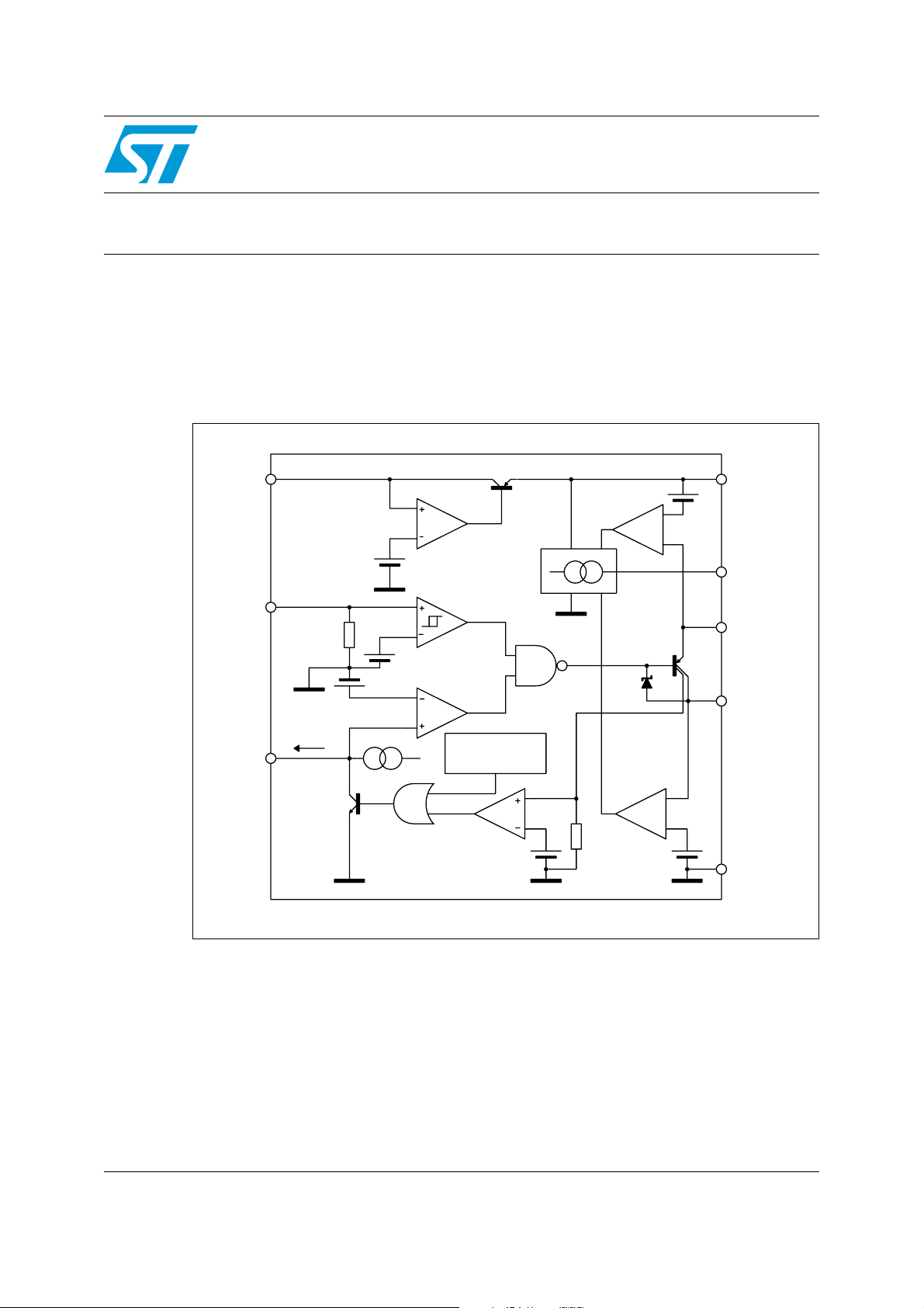
The TDE1707 is an industrial I.P.S. (intelligent power switch). Dedicated to proximity
detectors, it can deliver up to 0.5 A to a "configurable" load (load to battery or load to ground
configuration); see block diagram below.
Block diagram
VREG
+5V
IN
DELAY
6
5 V
5
Ri
1Mohm
2.6V
4V
4uA
3
5V
ISC
CMP
3mA LED
DRIVER
70V
THERMAL
SHUTDOWN
7
1
DRIVER
L.S. OUT
8
2
4
+Vs
LED
H.S. OUT
GND
December 2006 Rev 3 1/7
www.st.com

Obsolete Product(s) - Obsolete Product(s)
Effective filtering AN495
10nF
1mSec/nF
10nF
8
2
4
3
6
5
1 7
TDE1707
INPUT
VCC
GROUND
LOAD
10nf to 1uF
1 Effective filtering
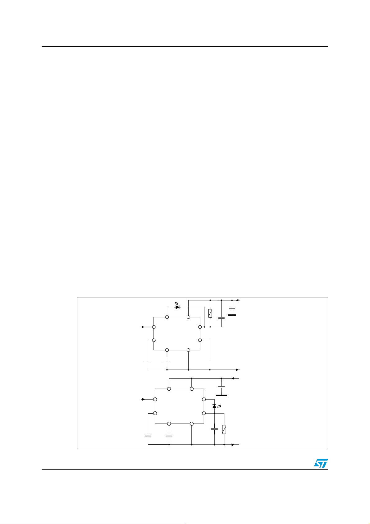
On the application circuit (Figure 1.) of the TDE1707 Data-Sheet, the use of filter capacitors
is recommended on both :
● The power supply (+Vs pin 7).
● The +5 V regulated voltage (Vreg pin 6).
– To understand the function of the Vreg capacitor, it is necessary to consider that
the Vreg pin makes available a regulated voltage that can be used to supply
external circuits (typically proximity detectors); but the TDE1707 itself, always uses
the Vreg to supply most of its internal circuits (see: Block diagram). Internally to
the TDE1707, Vreg supplies all the functional blocks, except the output power
transistor (and the Driver-Led, when the Led is connected as in "load to GND.
configuration").
– In the real application, the TDE1707 and associated circuitry, can be significantly
far away from the power supply and the long connection wires will act as a serial
inductance.
At power on, or at the turn-on of the power transistor, or in coincidence to load variations,
this inductance will react to the current variations with wide voltage variations. In proximity
sensor applications, for space reasons, the size of the filtering capacitors has to be reduced
as much as possible.
The voltage oscillation can induce two kind of problems in the circuit:
1. Overvoltage on the +Vs pin, connected to the +24V bus, that can exceed the TDE1707
rated limit.
2. Disturbances inside the circuit (TDE1707), because the noise immunity level is
exceeded with disruption of the input/output function.
Filtering the overvoltage on the +Vs is possible
Figure 1. Application circuit
High side load
VCC
10nF to 1uF
Low side load
LOAD
GROUND
INPUT
7 8
5
1
TDE1707
6
10nF
3
1mSec/nF
2
4
10nF
2/7

Obsolete Product(s) - Obsolete Product(s)
AN495 Effective filtering
only by an external capacitance between +Vs (pin7) and Ground (pin4) to limit voltage
spikes at the device’s rated values.
Immunity problems in the circuit are essentially related to the +5 V Vreg filtering, because
the noise on this voltage can induce errors in the low-voltage circuits.
The best solution, to avoid immunity problems, is to put the filter capacitor between Vreg
and Ground even if the Vreg dees not supply any external circuits. Compared to the +Vs
capacitor filtering effect, that also improves the immunity, the Vreg capacitor offers two
advantages:
1. The capacitive value can be significantly lower, for the same filtering effect, because
the Vreg filter does not have to sustain the load current variations.
2. The nominal voltage of the capacitor is lower (6 V instead of 25-50), so that the phisical
size of the capacitor is also smaller.
The higher effectiveness of filtering Vreg instead of +Vs is always evident. On average, in a
typical application, a capacitor put on Vreg can, with the same filtering effectiveness of a
capacitor on +Vs, be 20 times smaller in value.
Nonetheless, a capacitor on +Vs, although not of high value, is recommended. Its value
shall be adapted in accordance to the equivalent inductance of the supply connections and
of the value of the load.
For instance, the values used in the test circuit (Figure 2.) :
● 325 µH are too high to be found in pratice.
● 4.7nF on +Vs are barely sufficient with 325 µH (with 325 µH, 10nF would be
preferable).
● 4.7nF on Vreg are sufficient in most of the pratical cases.
● Using the test circuit shown in Figure 2., with the input trigger of the TDE1707 in pulsed
mode, the effect of the capacitor un Vreg (pin 6) can be noted in diagrams Figure 3.
and Figure 4.:
– Figure 3. shows the voltage, on +Vs (Ch1) and Vreg (Ch2), at turn-on and turn-off
edges, without the filter capacitor on pin 6.
– Figure 4. shows the same signals but with 4.7 nF capacitor connected between
Vreg (pin 6) and Ground.
The improvement of the immunity level and the low values of the capacitors makes the
suggested filtering solution the best for proximity detector application.
3/7

Obsolete Product(s) - Obsolete Product(s)
Effective filtering AN495
Figure 2. Test circuit
24V
325uH
LOAD 75ohm
4.7nF
8
Vs
LOW SIDE OUT
1 7
LED
OUT
2
HIGH SIDE OUT
4
GROUND
TDE1707
6
OUT
V.REG
IN
DELAY
5
3
4.7nF
50ohm DELAY CAP
4/7

Obsolete Product(s) - Obsolete Product(s)
AN495 Effective filtering
CH1
24V
CH2
5V
CH1 20V/div t = 20µSec/div
CH2 2V/div
ON
OFF
Figure 3. Voltage on Vs and Vreg without filter capacitor
CH1 20V/div t = 20µSec/div
CH2 2V/div
CH2
5V
CH1
24V
Figure 4. Voltage on Vs and Vreg with filter capacitor
ON
OFF
5/7

Obsolete Product(s) - Obsolete Product(s)
Revision history AN495
2 Revision history
Table 1. Revision history
Date Revision Changes
Nov-2003 1 First issue
14-Sep-2005 2 New template, no content change
14-Dec-2006 3 The document has been reformatted
6/7

Obsolete Product(s) - Obsolete Product(s)
AN495
Please Read Carefully:
Information in this document is provided solely in connection with ST products. STMicroelectronics NV and its subsidiaries (“ST”) reserve the
right to make changes, corrections, modifications or improvements, to this document, and the products and services described herein at any
time, without notice.
All ST products are sold pursuant to ST’s terms and conditions of sale.
Purchasers are solely responsible for the choice, selection and use of the ST products and services described herein, and ST assumes no
liability whatsoever relating to the choice, selection or use of the ST products and services described herein.
No license, express or implied, by estoppel or otherwise, to any intellectual property rights is granted under this document. If any part of this
document refers to any third party products or services it shall not be deemed a license grant by ST for the use of such third party products
or services, or any intellectual property contained therein or considered as a warranty covering the use in any manner whatsoever of such
third party products or services or any intellectual property contained therein.
UNLESS OTHERWISE SET FORTH IN ST’S TERMS AND CONDITIONS OF SALE ST DISCLAIMS ANY EXPRESS OR IMPLIED
WARRANTY WITH RESPECT TO THE USE AND/OR SALE OF ST PRODUCTS INCLUDING WITHOUT LIMITATION IMPLIED
WARRANTIES OF MERCHANTABILITY, FITNESS FOR A PARTICULAR PURPOSE (AND THEIR EQUIVALENTS UNDER THE LAWS
OF ANY JURISDICTION), OR INFRINGEMENT OF ANY PATENT, COPYRIGHT OR OTHER INTELLECTUAL PROPERTY RIGHT.
UNLESS EXPRESSLY APPROVED IN WRITING BY AN AUTHORIZED ST REPRESENTATIVE, ST PRODUCTS ARE NOT
RECOMMENDED, AUTHORIZED OR WARRANTED FOR USE IN MILITARY, AIR CRAFT, SPACE, LIFE SAVING, OR LIFE SUSTAINING
APPLICATIONS, NOR IN PRODUCTS OR SYSTEMS WHERE FAILURE OR MALFUNCTION MAY RESULT IN PERSONAL INJURY,
DEATH, OR SEVERE PROPERTY OR ENVIRONMENTAL DAMAGE. ST PRODUCTS WHICH ARE NOT SPECIFIED AS "AUTOMOTIVE
GRADE" MAY ONLY BE USED IN AUTOMOTIVE APPLICATIONS AT USER’S OWN RISK.
Resale of ST products with provisions different from the statements and/or technical features set forth in this document shall immediately void
any warranty granted by ST for the ST product or service described herein and shall not create or extend in any manner whatsoever, any
liability of ST.
ST and the ST logo are trademarks or registered trademarks of ST in various countries.
Information in this document supersedes and replaces all information previously supplied.
The ST logo is a registered trademark of STMicroelectronics. All other names are the property of their respective owners.
© 2006 STMicroelectronics - All rights reserved
STMicroelectronics group of companies
Australia - Belgium - Brazil - Canada - China - Czech Republic - Finland - France - Germany - Hong Kong - India - Israel - Italy - Japan -
Malaysia - Malta - Morocco - Singapore - Spain - Sweden - Switzerland - United Kingdom - United States of America
www.st.com
7/7
 Loading...