

Page 1
AN487
APPLICATION NOTE
INTRODUCTION TO A 10A MONOLITHIC SWITCHING
REGULATOR IN MULTIPOWER-BCD TECHNOLOGY
by C. Diazzi
The L497X series of high c urrent switching r egulator ICs exploit Multipower -BCD technology to achieve
very high output currents with low power dissipation – up to 10A in the Multiwatt power package and
3.5A in a DIP package.
Switched mode techniques led to t he develo pme nt of high efficiency c ircuits offering space s aving and a
reduction in costs, mainly of th e heatsink and output LC filter. For these applications a n ew technology,
called MULTIPOWER-BCD, has been developed which allows the integration on the same chip of isolated
power DMOS elements, Bipolar transistors and CMOS logic.
The technology is particularly suitable for the problems rising in the switch mode field, due to the characteristics of high efficiency, fast switching speed, no secondary breakdown of the power DMOS element.
The great flexibility that we ha ve at our disposal for the c hoice of the s igna l an d drivin g s ections com ponents allows optimization and compactness of the system. With MULTIPOWER-BCD it has been possible
to implement the family L497X, a new series of fully integrated switching regulators suitable for DC-DC
converters working in Buck configuration. The complete family consists of five devices which differ each
other only by the output current v alue (2A, 3.5A, 5A, 7A, 10 A) they can deliver to the load. The devices
rated at 2A and 3.5A are assembled in Power Dip (16+2+2), while the others are assembled in the
Multiwatt15 package. Each device integrates a DMOS output power stage, a control section, limiting current and supervisor functions like Reset and Power Fail signal for microprocessors applications.
Output voltage can be adj usted starting from the internal reference voltage (5. 1V) up to 4 0V, allowing a
maximum output power of 80W for the 2A version a nd of 400W f or the 10A vers ion. M aximum o perat ing
supply voltage is 55V.
THE TECHNOLOGY
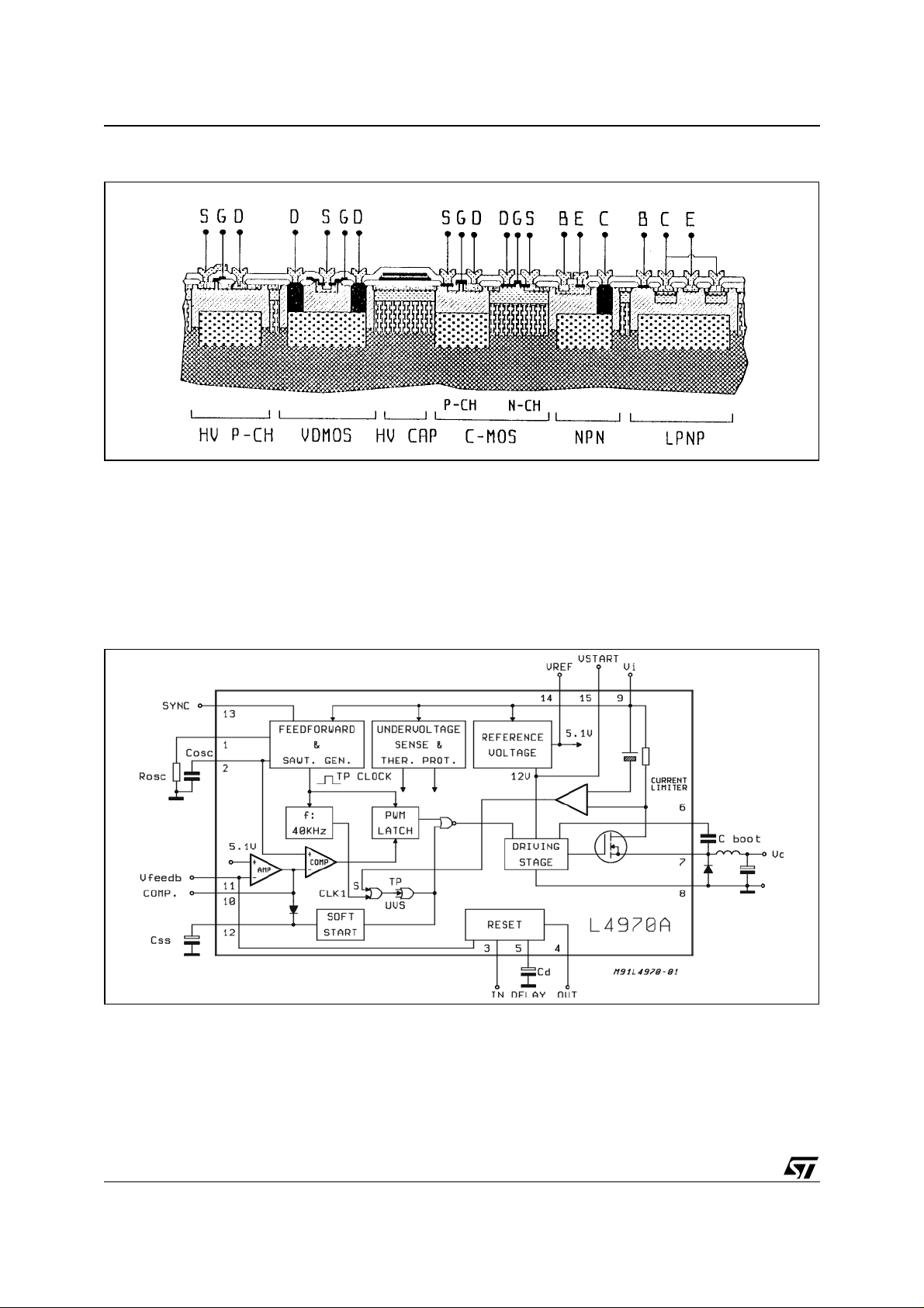
The technology architecture is bas ed on the vertical DMOS sil icon gate process that allows a chan nel
length of 1.5 micron ; using a junction isolation technique it has be en possible to mix on the same chip
Bipolar and CMOS transistors along with the DMOS power components (Fig. 2). Figure 1 shows how this
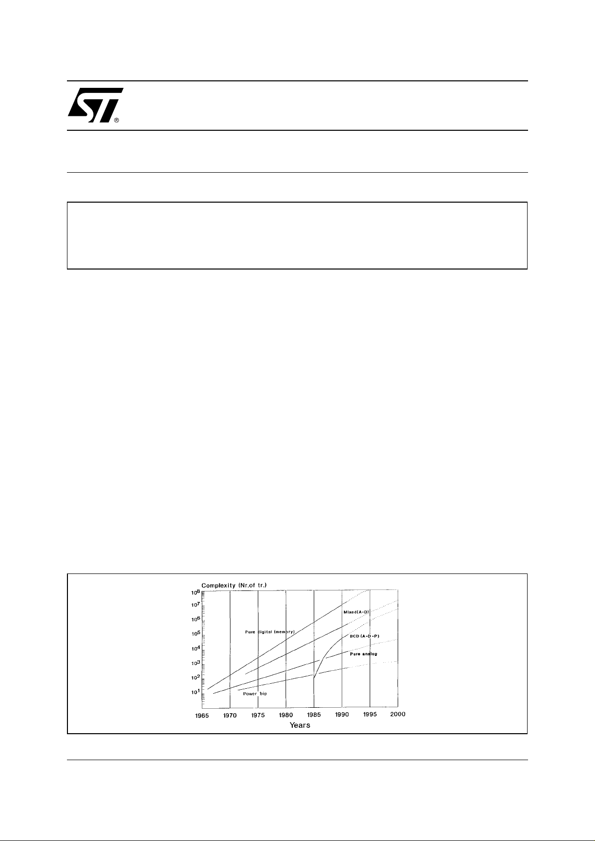
process brings a rapid increase in power IC complexity compared to conventional bipolar technology.
Figure 1. BCD process and increase in power ICs complexity.
November 2003
1/13
Page 2
AN487 APPLICATION NO TE
Figure 2. Cross section of the BDC mixed technology.
In the 70’s class B circuits and DC circuits allowed output power in the range of 70W. By 1980 ,with the
introduction of switching techniques in power ICs, output powers up to 200W were rea ched; with BCD
technology the output power increased up to 400W.
FUNCTIONS AND BLOCK DIAGRAM
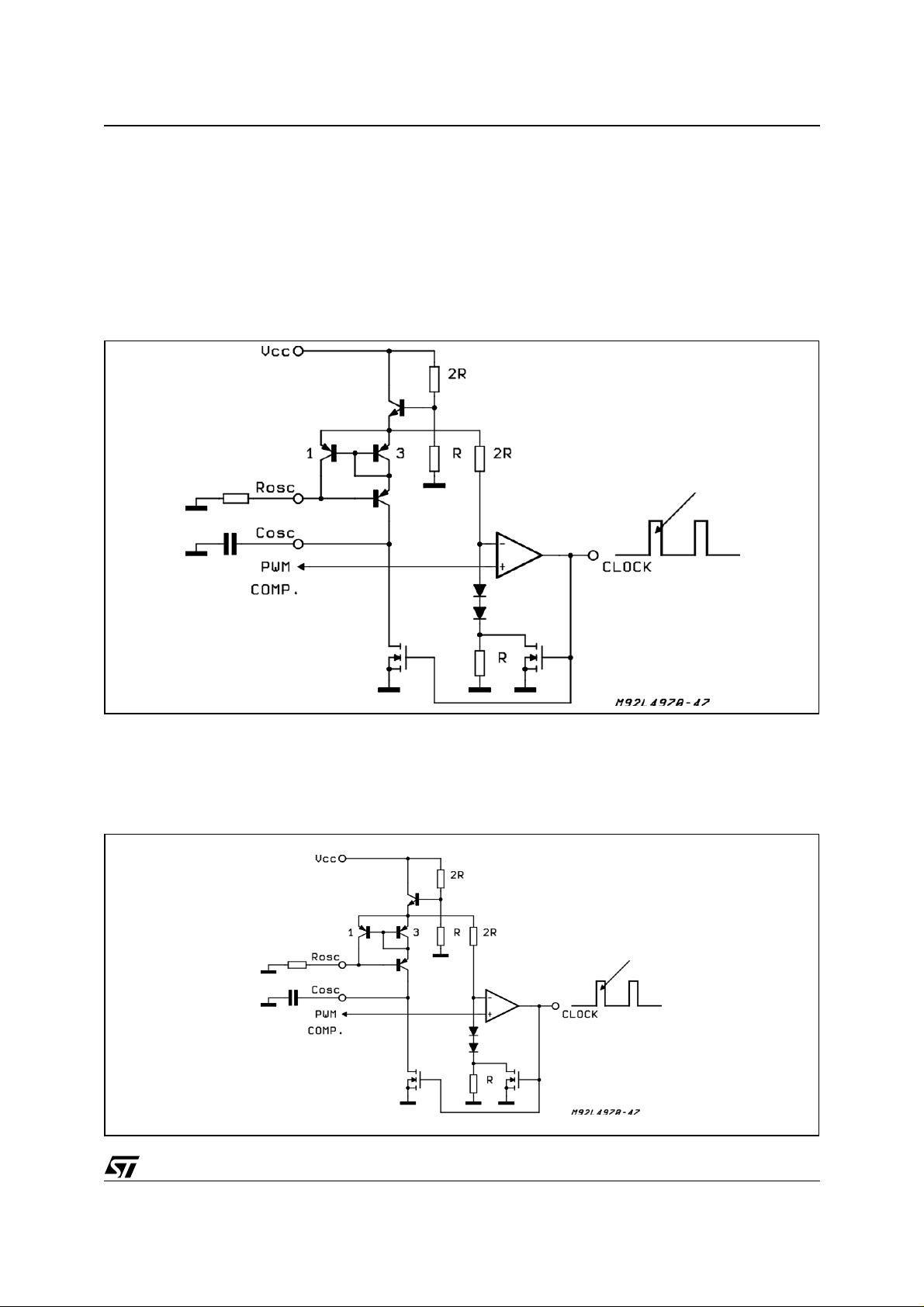
The complete block diagram of the hi gh power L4970A is shown in fig.3. Each bl ock is analysed in the
follo wing .
Figure 3. Block diagram of the 10A monolithic regulator L4970A.
POWE R SU PPLY
The device is provided with an internal stabilized p ower supply ( Vstart =12V ), that p rovides the supply
voltage to the analog and digital co ntrol blocks and also the suppl y vo ltage to th e bootstrap section. The
Vstart voltage supplies also the internal Reference Voltage section that provides accurate 5.1V voltage to
the control loop. Through trimming techniques the 5.1V reference is within +- 2% limits.
2/13
Page 3
AN487 APPLICATION NOTE
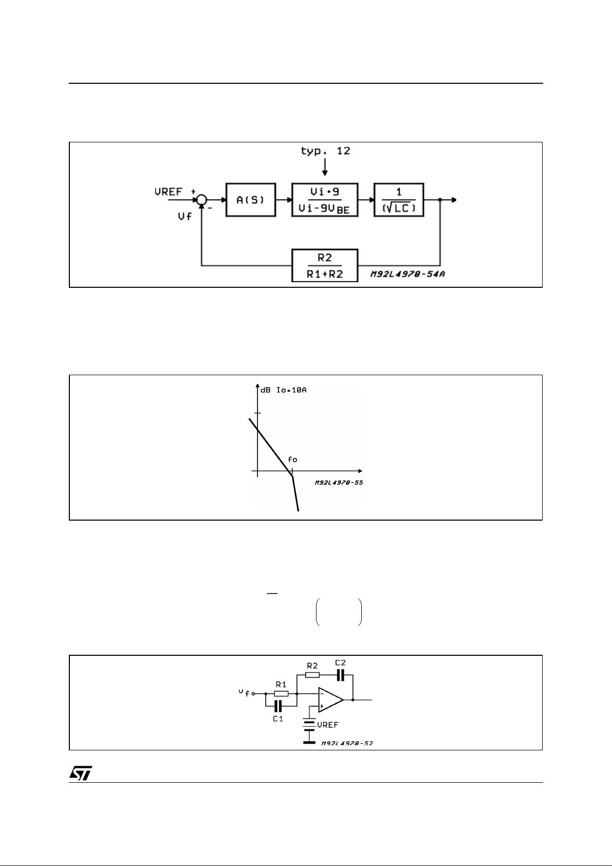
OSCILLATOR and FEDF ORWARD
The oscillator block (fig.4) generates the sawtooth waveform that sets the switching frequency of the sys-
tem. The signal, compared with the output voltage of the error amplifier, generates the PWM signal to be
sent to the power output stage. The oscillator features a voltage feed-forward technique which is completely integrated and doesn’t require any external component. Feed-forward function works in the supply
voltage range 15-45V. The rate of increase of the sawtooth wavw-form is directly proportional to the input
voltage Vcc. As Vcc increases, the output pulse-width (transistor on-time) decreases in such a manner as
to provide a constant "volt-second’ product to the inductance(fig.5).
Figure 4. Oscillator circuit
From fig.5 it is shown that the duty cycle c hanges due to the ramp increase when V cc increases. T he error
amplifier output doesn’t have to change to keep the loop in regulation. This feature increases significantly
the line regulation performance.
Figure 5. Voltage Feeforward waveform.
3/13
Page 4

AN487 APPLICATION NO TE
A resistor, between Rosc and GND , define s a curr ent that is mirrored in terna lly to c harge the oscillator
capacitor on the Cosc pin. The voltage at pin.Rosc is a function of Vcc value for the implementation of the
feed-forward fun ction (oscillator slope proportion al to Vcc ). A compa rator is sensing the voltage a cross
Cosc capacitor and dis-carge it when the ram p exceedes an u pper threshold proportional to V cc for the
implementation of the feed-forward function. The Cosc discharge current is internally controlled at a value
of about 20 mA. The lower threshold of the comparator is about 1.3V (2VBE). Here are reported basic
equations for the oscillator:
V
9V
–
I
CHARGE
V
TH.HIGH
CC
------------------------------- -=
V
CC
------------------------------- - 2V
BE
R
OSC
I
DISCH
–
9
for 15V ≤ V
@ 20m A (2)
9V
BE
+=
BE
≤ 45V (1)
CC
for 15V ≤ V
≤ 45V (3)
CC
V
TH. LOW
F
SWITCH
Note that formula (5) does not take in account the discharge time of C
at high F
SWITCH
(200 KHz), and that is dependent on C
T
DISCH
--------------------------------------------- ------------------------------- -=
= 2VBE (4)
9
--------------------------------
≅
R
OSCCOSC
, that is not negletable working
OSC
⋅
osc
OSC
V
T H.HIGHVTH.LOW
–()C
value.
20m A
(5)
(6)
By whic h :
----------------------------------- ----------------- -
R
oscCosc
------------------------- - T
1
+
9
DISCH
(7)
During the discharge time of Cosc a clock pulse is generated t hat is av ailable on pi n.SYNC and that can
be used to synchronize max 3 dev ices of the sam e f ami ly. See also fig. 6 and fig. 7 for the switchin g frequency versus value of R4 (R
osc
).
PWM
The comparison between oscillator sawtooth and error amplifier output generates the PWM signal that
feeds the driving stages. A PWM latch structure is implemented to avoid multiple pulses that could be dangerous for the power stage. A maximum duty cycle limitation is impleme nted in the PWM s tage. Such
limitation is obtained by the synchronization pulse generated in the oscillator section during the Cosc discharge time. When the pulse is present the driver is inhibited. In this way even if the error amplifier output
completely overcomes the oscillator sawtooth, the power stage can not work in DC conditions, but is
switched off during the clock pulse allowing a maximum duty cycle tipically in the range 90 - 95 % .
SOFT START
Soft start (see fig.8) is an essential function for correct start-up and to obtain a monotonically increasing
output voltage, without overstressing the output power stage. Soft start operates at the start-up of the system and after the intervention of thermal protection. The function is realized through a capacitor connected
to soft start pin, which is charged at constant current(about 100uA) up to a value of about 7V.
During the charging tim e , t hrough PNP transisto r Q1 t he voltage at the output of the t rans conduc-tance
amplifier is forced to increase with the same rising speed of Css cap acitor. As the capacitor is c harged,
4/13
Page 5

AN487 APPLICATION NOTE
the PWM signal begins to b e generated as soon
as the error amplifier output voltage crosses the
ramp; the power stage starts to switch with steadily increasing duty cycle (fig.9).
Figure 6. Switching frequency vs. Rosc
(L4970A/77A/75A).
Figure 8. Soft start circuit
Figure 7. Switching frequency vs. Rosc
(L4972A/74A).
The charge of the soft-start capacitor is started every time the system begins to work after an anomalous condition occurred (undervoltage and
thermal protection). The Css discharge current is
in the range of about 20mA.
Figure 9. Soft start waveforms
5/13
Page 6

AN487 APPLICATION NO TE
Figure 10. Error amplifier circuit
UNDERVOLTAGE LOCKOUT
The chip features a complete built-in un der v oltage lock out prot ection, keeps the power output stag e off
up to the moment Vcc reaches 11v, with an hysteresis of 1V. After reaching the 11V value the system
starts with the soft start feature.
ERRO R AMPLI F I ER
The error amplifier is a transconductance Operationa l Amplifier featuring a current o utput. The simplified
schematic is represented in fig.10. T he basic characteristics of the uncom pens at ed o perat ional amplifier
are the following:
–G
= 4mA/V,
M
= 2.5Mohm,
–R
o
=80dB,
–A
Vo
–I
source/sink
–I
Input
= 200µA
Bias Current = 0.3µA
The frequency behavior of the uncompensated amplifier is reported in fig.11.
Figure 11. Ope n l oop gai n ( error amplifie r only ).
6/13
Page 7

AN487 APPLICATION NOTE
Neglecting the high frequency be havior (in the hy -potesis that in the overall f requency com pensation of
the loop the second pole of the operational amplifier is far below the 0 dB axis), we can make a first order
approx. by which the error amplifier can be schematized by the equivalent circuit of fig.12.
Figure 12. Error amplifier equivalent circuit.
by which
R
o
---------------------------- -
AVs() G
⋅=
M
1SRoC
+
o
where C
= 3pF.
o
The error amplifier is inserted in the regulation loop and c an be easily com pensated, thanks to i ts high
output impedance, with a network between its output and ground. The typical compensated netw ork is
shown in fig.13.
Figure 13. Compensation network of the error ampli fier.
The transfer function is:
AVs() G
---------------------------------------------------------------------------------------------------------------------- -
+()
⋅=
v
2
S
R
C
R
C
o
o
SRoCcRoCoRcC
c
c
o
++()1++
c
Ro1SRcC
In the hypotesis that Rc<Ro and Cc>Co, the Bode diagram of the compensated amplifier is reported (see fig.14).
Figure 14. Bode plot showing gain and ph ase of comp ens ated erro r am plifier.
7/13
Page 8

AN487 APPLICATION NO TE
The compensation network introduces a low frequency pole and a zero that usually is put at the frequency
of the resonant pole of the output LC filter. The second high frequency pole is usually at a frequency of no
interest. If needed , more sop histica ted comp ensati on circuits can be used by feedbac k wit h the opamp.
An example is shown in fig.15.
Figure 15. One pole, tw o z ero compensation net work.
Such a configuration introduces a low frequency pole and two zeros Z1 = 1/2ΠR1C1 and Z2 = 1/2ΠR2C2.
Note that due to the high out put impedance it is present als o a sec ond pole p2 = gm/2PC1. Usual ly it is
better to use the highest possible value for R1, to have a low value for C1 in such a way to put p2 at the
highest frequency. Limitations to R1 value are put by offset voltage due to opamp. input bias currents.
If a resistive divider is used at the output of the power supply, for voltages higher than 5.1V, it is possible
to introduce a second zero with the network of fig.16.
Figure 16. Compensation network for output voltages higher than 51V.
Such a configuration introduce 2 zeros at:
Z
1
1
---------------------- -= Z
2ΠR
;
cCc
2
-----------------------=
2 Π R
1
1C1
and 2 poles at:
P
1
1
---------------------- -= P
2 Π R
; ;
oCc
---------------------- -= Rx
2
2 Π R
1
xC1
R
1R2
--------------------=
R1R2+
8/13
Page 9
AN487 APPLICATION NOTE
APPLICATION EXAMPLE
Figure 17. Block diagram used in stability calculation.
Consider the block diagram of fig.17, repres enting the internal control loop section, with the appl ication
values:
Fswitch = 200KHz, L = 100µH, C =1000µF, Po=50W, Vo =5.1V,
Io =10A and Fo = 500Hz. G
Figure 18. Frequen cy behavior of the circ uit of fi g 17.
= PWM × Filter
loop
The system requires that DC gain is maximum to achieve good accuracy and line rejection. Beyond this
a bandwidth of some KHz is usually required for a good load transient response. The error amplifier transfer function must guarantee the above constraints. A compensation network that could be used is shown
in fig.19.
As()
+()1sR2C
sR
1C1
1C1
------------------------------------------------------------------=
+()
+
1s
C
1
--------
G
M
2
1sR
Figure 19. Compensation network.
9/13
Page 10

AN487 APPLICATION NO TE
Figure 20. Bod e pl ot of th e regulation loo p wi th t he com pensatio n net work of fig. 19.
The criterium is to define Z1, Z2 close to the resonant pole of the output LC filter. The Gm/2PC1 pole must
be placed at a frequency at which open loop gain is below 0 dB axis (Fig. 20).
CURRENT LIMITATION
Current limitation is implemented intrnally to the chip and doesn’t need any external component.
The output current is sensed by an internal resistor in series with the drain of the power transistor. On chip
trimming guarantees +10% accuracy on the value of peak current limitation.
Current limit protection works pulse by pulse with lowering of tnhe switching frequency. Fig.21 shows cir-
cuital implementation of current protection.
Figure 21. Current protection circuit.
10/13
Page 11

AN487 APPLICATION NOTE
When the comparator sens es an ov ercurrent, the
flip-flop is set and an internal inhibit signal is generated. The flip-flop remains set until next reset
clock pulse coming from the internal 40 KHz oscillator. After the reset pulse the regulation loop
takes the control of the system and the output current begins to increase to the load value at the
switching frequency of the master clock. If the
overload condition is still present the protection cycle repeats. This mixed, pu lse by pulse, lowering
frequency current protection method, assures a
constant current output when the system is in
overload or short circuit and all ows t o i m plement a
reliable current limitation even at high switching
frequency (500 KHz) reducing the problems of signal delay through the protection stage. Fig.22
shows behavior of the inductance current when
the system is in overload.
Figure 22. Overload inductance current.
The internal 40 KHz oscillator is synchronized with
the master clock. When the syst em works with the
master clock at a lower frequency of the internal
clock, than the internal clock tracks the master frequency. This assures t hat t he f requency does not
increas during overload.
POWER FAIL-RESET CIRCUIT
The L4970A include a voltage sensing circuit that
may be used to generate a power on power off reset signal for a microprocessor system. The circuit
senses the input supply voltage and the output
generated voltage and will generate the requ ired
reset signal only when both the sensed voltages
have reached the required valu e for correct system operation. The Reset signal is generated after
a delay time programmable by an external capacitor on the delay pin. Fig. 23 shows the circuit implementation of Reset circuit. The supply voltage
is sensed on an external pin, for program mability
of the threshold, by a first comparator. The second
comparator has the reference threshold set at
slightly less the ref. voltage for the regul ation circuit and the other input connected internally at the
feedback point on the error amplifier. This allows
to sense the output regulated voltage. When both
the supply voltage and the regulated voltage are in
the correct range, transistor Q1 turns off and allows the current generator to charge the delay capacitor. When the capacitor voltage reaches 5V
the output Reset signal is generat ed. A latch assures that if a spike is present on the sensed voltage the delay capacitor discharges completely
before initialization of a new Reset cycle. The output gate assures immediate take of reset signal
without waiting for complete discharge of delay capacitor. Reset output is an ope n collec tor transistor capable of sinking 20mA at 200mV voltage.Fig. 24 shows reset waveforms.
Figure 23.
11/13
Page 12

AN487 APPLICATION NO TE
Figure 24. Reset and power fail waveforms.
THE POWER STAGE
A simplified schematic of the output stage along with the external filter components is shown in fig.25.
Power stage and associated driving circuits are among the most critical components to achieve good per-
formances at high switching frequency. An external bootstrap capacitance, charged via diode D1 at 12V,
is needed to provide the correct gate drive to the power DMOS N-channel transistor. The driving circuit is
able to deliver a current peak of 0.5A, during turn on and turn off phases, to the gate of power DMOS transistor. The circuit-described shows commutation times of 50ns.
Figure 25. Power stage circuit.
The five devices of L497X family differentiate each other only for the level of current protection, while the
control part is the same and power dev ice area is the sam e to gua rantee low power dissipa tion also for
low current versions in DIP package.
Table 1 and fig. 26 shows electrical characteristics of the power DMOS implemented in the chip.
12/13
Page 13

Table 1.
B
> 60V at ID = 1mA VGS = 0V
VDSS
AN487 APPLICATION NOTE
R
R
V
= 100mΩ at ID = 10A Tj = 25°C VGS = 10V
DS(ON)
= 150mΩ at ID = 10A Tj = 150°C VGS = 10V
DS(ON)
= 3V at ID = 1mA
TH
THERMAL PROTECTION
The thermal protection function operates when the junction temperature reaches 150°C; it acts directly on
the power soft start capacitor, discharging it. The thermal protection is provided with hysteresis and therefore, after an intervention has occurred, it is necessary to wait for the junction temperature to decrease of
about 30°C below the intervention threshold.
Figure 26. Gate-charge curve for the power DMOS.
Information furnished is believed to be accurate and reliable. However, STMicroelectronics assumes no responsibility for the consequences
of use of such information nor for any infringement of patents or other rights of third parties which may result from its use. No license is granted
by implic ation or o th erwise un der any patent or patent ri ghts of STM i croelectronics. Specifications me ntioned in this publication are subje ct
to change without notice. This publication supersedes and replaces all information previously supplied. STMicroelectronics products are not
authorized for use as c ri t i cal components in life support dev i ces or systems without express wri t ten approval of STMic roelectronics.
The ST logo is a registered tradem ark of STMi croelectr oni cs.
All other n am es are the property of their resp ective owners
© 2003 STMi croelectronics - All ri ghts reser ved
Australi a - B elgium - B razil - Canada - China - C zech Republ i c - Finland - F rance - Germany - Hong Kong - India - Israel - Italy - Japan -
Malaysia - Malta - Morocco - Singapore - Spain - Sweden - Switzerland - United Kingdom - United States
STMicroelectronics GROUP OF COMPANIES
www.st.com
13/13
 Loading...