

Page 1

AN471
APPLICATION NOTE
SMART POWER TECHNOLOGIES FOR
POWERTRAIN & BODY ELECTRONICS
by R. Ferrari
Smart power ICs are becoming increasing by common in automotive powertrain and body electronics.
This note provides a general introduction to the subject.
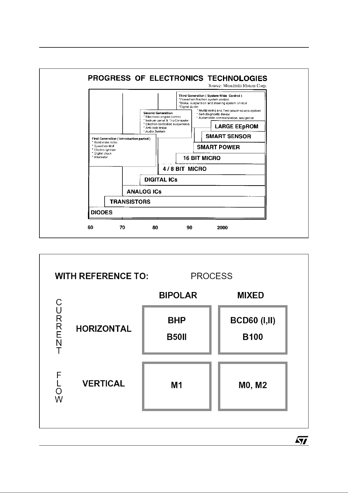
As is well known, electronics is slow ly but progress ively invading ev er y part of the automotive env ironment ( figure 1); entering first in the car radio, it has extended progressively and is now present in all of the subsystems
of an automobile. For those people who prefer a "historical" approach, the evolution of auto electronics has been
divided into three main sections, each subdivided into various phases , correlated with the state of the art in general electronics at that time. Today, at the beginning of the 90’s we are in the SMART POWER phase, and it is
precisely that which we intend to discuss briefly here (see fig. 2).
We will look at, first of all, so me definiti ons: sm art power or i ntelligent power indicates those fami lies of integr ated circuits which include both logic control circuits and components capable of delivering a significant amount
of power to a generic load. In numbers, a ci rcuit can be c onsidered sm art power if it i s able to deliver mor e than
0.5A to the load, or of withstanding more than 50V, or able to supply a power of at least 1W to the load.
Over the years ST Microelectronics has developed v arious t echnologies that a llow the reali zation of smart p ower
circuits (figure 3). The simplest way to classify these technologies is to refer to the process type, which can be
purely bipolar or mi xed, that is, includi ng on a sin g le pie ce of sili con both MOS struc tures (of c ontrol and power)
and bipolar structures. Another method (figure 4) is to examine the way in which the current flows through the
power section; horizontal, with the current entering and leav ing through the upper surface, or vertic al, where the
current enters through the upper surface and leaves thr ough the lower surface; for this lower connection i nstead
of wire the tie bar of the package is used.
The choice of one technology rather than another depends on various elements (figure 5) but simplifying as far
as possible the criteria, we can say that vertical technologies can guarantee, for a given area, lower resistances
but they have the limitation of being able to include just one power device per circuit (or more than one, but always with the collectors or drains short-circuited); while
Figure 1. Electronics in present and future automobiles.
SAFETY & CONVENIENCE BODY CONTROL POWER TRAIN DRIVER INFORMATION
Rear Window Defogger Cruise Control Ignition Digital Gauges
Climate Control Intermittent Wipar Spark Timing Digital Clock
Keyless Entry Antitheft Devices Voltage Regulator Multitons Alarms
Automatic Door Lock Electr. Suspension Alternator Engine Diagn. Results
Light Drimmer Electr. Steering Idle Speed control Service Reminders
Traction Control Multiplex Wiring Turbo Control Miles to Empty
Antiskid Braking Module to Module Emission System Shift Indicator
Window Control Communications Transmiss. Control Head-up Display
Memory Seat Load Sensit. Braking Diagnostics CRT Display
Heasted Windshield Hard/Soft Ride Control Audio Annunciator
Voice Controlled Trunk
Airbag Restraints
November 2003
1/10
Page 2
AN471 APPLICATION NO TE
Figure 2.
Figure 3. Smart Power Technol og ies Matrix .
2/10
Page 3

Figure 4. Integrated DMOS structures.
1OR MORE HV LDMOS DEVICES WITH COMMON SOURCE
AN471 APPLICATION NOTE
MANY POWER VDMOS DEVI CES AN Y CONFIGURAT ION
1 OR MORE HC VDMOS DEVICES WITH COMMON DRAIN
3/10
Page 4

AN471 APPLICATION NO TE
Figure 5. Smart Power Technology Matrix selection criteria.
Figure 6. Multiple independent Power Structures realized with Horizontal Technology.
Figure 7. Bo nding wire features.
WIRE
GOLD
GOLD
ALUMINIUM
ALUMINIUM
ALUMINIUM
4/10
DIAMETER
(micron)
25
51
178
254
381
RESISTANCE
(mOhm/mm)
45
11
1
0.5
0.2
D.C. CAPABILITY
(Ampere)
in plastic package
1.25
2.50
15
28
43
Page 5

AN471 APPLICATION NOTE
horizontal technologies make it possible to have power structures that are completely independent (f igure 6). It
is therefore evident that a vertical technology will give excellent results in the design of a light switch, while a
horizontal technology will be equally well suited to the design of a multiple actuator.
It is important at this point to underline that a smart power circuit does not consist of just silicon technology, but
relies heavily on package tec hnology. In fact it is well known that a signal device is bonded using gol d wires with
a diameter of 25 microns; however, gold wire can be used effectively up to diameters of 50 microns, which allows reliable operation with curr ents up to 2A, provided that the wire is su rrounded by resin (the curr ent capacity
drops by 50% for wires in free air -- that is, in the case of hermetic packages, When, however, one has to deal
with very high currents (more than 5A in single-point injection actuators, and more than 10A for windowlift motors) gold wires are no longer usable for obvious cost reasons so it is necessary to turn to aluminum wires (figure
7) with a diameter from 180 microns to 375 microns; clearly in this case it will be necessary to have adequately
dimensioned bonding pads on the die, with a significant waste of silicon area.
Optimization is obtained with a mixed bonding technology where signal pads are bonded with thin gold wires
and power pads with thick aluminum wires (figure 8). A further optimization is obtained by orienting the pads in
the pad-to-bond-post direction. But while we are speaking of power it is also important to speak of packages
(figure 9). These packages are part of a long tradition of TO-220 type packages (with 3, 5 and 7 pins) but recently new needs in assembly are bringing important evolutions of the classic tab packages. Devices completely
encapsulated in completely isolate d packages -- called Isowatt --are already in production; in these devices isolation up to 1000V is obtained with a mini mum reduction in the junction-to-cas e thermal resistance. On the other
hand, the practice of using clips, rather than screws, for mounting pac kages is becoming al ways more common,
both to save space and to obtain b etter long-term rel iabili ty i n thermal conduc tion. This has led to the TABLESS
isolated package which accumulates the previous two needs, while for surface mounting a non-isolated package with a junction-case thermal resistance less than 3’C/W is in development in our laboratories and will be
available in industrial quantities in 1991.
Now that we have examined the means that technology places at our disposition, both in diffusion and in assembly, we can now examine what typical structures smart power processes will allow us to make, and which
kind of circuit will normally be driven by each structure (figure 10).
Figure 8. Mixed Bonding Technology.
5/10
Page 6

AN471 APPLICATION NO TE
Figure 9. Power package Matrix.
Figure 10. Intelligent power actuators basic configuration .
Figure 11. Intelligent power actuators basic protection.
1) The typical, so-called High Side configuration, in which the actuator is located between the supply and the
load, is traditionally used in the s upply of resis t ive loads , typically lamps , but is also suit able for mono-dir ectional motors.
2) When the actuator is between the load and the ground of the supply system we have a "low side" configuration, very common for driving inductive loads such as, for example, the solenoids that control the opening
of valves (injectors, ABS system, automatic transmission), but also ignition coils.
6/10
Page 7

AN471 APPLICATION NOTE
3) Finally, when we have to drive a motor that rotates in both directions it will be necessary to use a bridge
structure; the choice between integrating the whole bridge or just half of it clearly depends on the current
involved. Today’s technology allows us to realize efficiently a complete bridge to drive a door lock motor,
while it is necessary to use two half bridges if the load is a windowlift.
In all of these structures there will always be integr ated a certain number of protection ci rcuits, to guarantee survival of the device in the presence of possible failures in the surrounding ambient (figure 11).
These include, to name a few, the automatic shutdown when the silicon reaches a critical temperature (which
can be caused not only by a short circuit in the load or its connections, but also by the degradation of thermal
contact between the device and its heatsink). Today, in certain applications such as fuel injection this automatic
shutdown tends to be replac ed wi th a war ning s ignal, which informs the co ntrol unit when a critical situation has
been reached, leaving the unit itself to decide what to do (for example, reduce performance to guarantee functionality).
Another very common structure is output current limiting, even in the case of a load short circuit. Usually the
intervention of the limitation circuit is accompanied by a diagnostic signal that is made available for the control
system. Finally, in some devices a circuit is included that is able to detect overvoltages in the supply system,
disabling the output stage and placing it in the best conditions to support the overvoltage.
Given the above, we will now describe a practical case with the aim of identifying how the design time can be
optimized through a suitable interaction between the system designer and the silicon manufacturer.
The circuit shown in figure 12 is a dual low-side actuator desi gned to drive two independent loads wi th curr ents
up to 3A each (typically injectors).
Figure 12. Dual 3A Low-side Actuator.
The technology employed is mixed (bipolar/CMOS/DMOS) with a horizontal current flow (BCD60); if we pass
from the photograph to a topographical diagram of the silicon (figure 13) it becomes immediately evident that
the chip is divided into a limited number of macroblocks, for each of which it is easy to attribute project leadership. In fact it will be an essential task of the system designers to define the cr iteria for the driving of the actuator
as it is to define the malfun ctions for whi ch the activ ation of a diagno stic signal is necessa ry. O n the ot her hand
it is indisputable that only th e sili con desi gner can optimi ze the des ign of the pow er secti on and take adv antage
of structures already available in his library to realize those functions which are necessary and also repeated
frequently in different devices. The system designer, too, can take considerable advantage from the use of cell
libraries so the total desi gn time can be reduc ed to a mini mum (7-9 months from the s t art of the design to wor king silicon), reducing significantly the gap traditionally existing between a dedicated circuit (full custom) and a
semicustom circuit obtained from gate arrays or standard cells.
7/10
Page 8

AN471 APPLICATION NO TE
Figure 13. Expertise partitionin g when desi gnin g a smart po wer actu ator.
A brief glance at another two circuits, each representative of a technology described above. In the first we see
a highly-innovative circuit for use in ignition systems. This is the VB020 (figure 14), a circuit realized in mixed
vertical technology (M2) able to drive directly the primary of the ignition coil, combining a darlington with a vertical current flow with a driver circuit and TTL/CMOS compatible control circuit (figure 15). In the device are integrated circuits to limit the collector voltage (fixed at 450V max).
We conclude this series of examples with the L9937 (figure 15), a bridge circuit designed to drive a door lock
motor and therefore capable of delivering continuous currents of 6A with starting peaks up to 12A. The device
is realized in horizontal bipolar technology and, as appears in the photograph, is almost entirely occupied by
four large power transistors that constitute the output stages of the circuit. In this case, too, you can see the
mixed bonding (gold for the signal wires, aluminum for power wires) and the pads oriented to optimize silicon
area. In the block diagram (figure 16) you can see a chain of diodes which has the function of monitoring the
temperature of the chip. This brief introduction to smart power technologies would not be complete if it did not
dedicate a few words to the price th at the customer must pay to buy circ uits of this type. In fact a typical ques tion
that semiconductor companies frequently hear is "How much does a square millimeter of smart power silicon
cost?". Since the price of a square millimeter of sili con depends on the total area of the chip I believ e that it can
be a pleasant surprise to discover that even for fairly sizable chips -- that is, up to 25/6mm
2
mm
increases very little (about 25%). The curve of figure 17 gives the trend for areas between 5 and 50mm
and, though based on a theoretical calculation, follows closely the present commercial reality. Obviously the
graph reflects the current state of the art; if only three years ago the elbow of the of the curve had been moved
violently to the left without arriving at saying that the evolution will continue indefinitely with the same speed, it
is however reasonab le to e xpect i n the nex t few years a further extension of the li near zone at least towards the
40mm2 region. As for the meaning of "1mm
2
of silicon", several possibilities are given at the foot of the table.
There is another way to evaluate the price of a smart power circuit, and this is to estimate the price for each
ampere delivered to the load. This method of calculation is less rigorous and can be plotted as a graph assuming
as size reference the percentage of silicon dedicated to power compared to the total area of the chip. The line
shown in the figure 18 graph indicates that one ampere costs approximately 30 cents but can rise to 45 cents
for circuits containing particularly complex control and diagnostic logic, and it can fall to 15 cents for devices
consisting essentially of only power stages. It must be underlined that two consumer devices (L552 and
TDA2005 -- both audio power amplifiers) for which we can assume stable specifications, mature technologies
and ample markets, lie exactly on the curve. This should be indicative of the final trend for automotive devices
which are as yet young devices in a young market.
2
-- the price of each
2
8/10
Page 9

AN471 APPLICATION NOTE
Figure 14. Fully integrated high voltage darlington for electronic ignition.
■ PRIMARY COIL VOLTAG E UP
TO 450V
■ COIL CURRENT LIMIT IN-
TERNALLY SET TTL/CMOS
COMPATIBLE INPU T
■ BUILT-IN COLLECTOR-EMIT-
TER VOLTAGE CLAMPING
■ OVERVOLTAGE PROTEC-
TION OF THE DRIVING CIRCUIT
■ FULLY INSULATED FIVE
LEAD POWER PACKAGE
Figure 15. Die of VB020
9/10
Page 10

AN471 APPLICATION NO TE
Figure 16. Full bridge motor driver.
■ 6A OUTPUT CURRENT
■ LOW SATURATION
VOLTAGE
■ VERY LOW CONSUM-
TION IN OFF STATE
■ OVERLOAD DIAGNOS-
TIC OUTPUT
■ INTERNAL TEMPERA-
TURE SENSOR
■ GROUNDED CASE
Figure 17. Smart power silicon Figure 18. Smart power devices
Information furnished is believed to be accurate and reliable. However, STMicroelectronics assumes no responsibility for the consequences
of use of such information nor for any infringement of patents or other rights of third parties which may result from its use. No license is granted
by implic ation or oth erwise under any patent or pat ent rights of STMicroelectronic s. Specifications mentioned in this pub lication ar e subject
to change without notice. This publication supersedes and replaces all information previously supplied. STMicroelectronics products are not
authorized for use as critical comp onents in life support devi ces or systems wi thout express written approval of STM i croelectronics.
The ST logo is a registered tradema rk of STMicroelectronic s.
All other n am es are the pro perty of their respectiv e owners
© 2003 STMi croelectro ni cs - All rights reserved
Australi a - B elgium - Brazil - Canad a - China - Czech Republic - Fi nland - France - Germany - Hong Kong - Indi a - Israel - Italy - Japan -
Malaysia - Malta - Morocco - Singapore - Spain - Sweden - Switzerland - United Kingdom - United States
STMicroelectronics GROUP OF COMPANIES
www.st.com
10/10
 Loading...