

Page 1
AN469
APPLICATION NOTE
USING THE L6506 FOR CURRENT CONTROL
OF STEPPING MOTORS
by Thomas Hopkins
Chopper-type current control circuits improve the performance of motor drives. This note shows how
this can be done simply using the L6506 current controller IC.
The L6506 is a linear integrated circuit designed to sense and control the current in stepping motors and other
similar devices. When used in conjunction with power stages like the L293, L298N, or L7180 the chip set forms
a constant current drive for inductive loads and performs all the interface functions from the control logic through
the power stage.
The L6506 may be used with either two phase bipolar or four phase unipolar motor configurati ons. The circuit
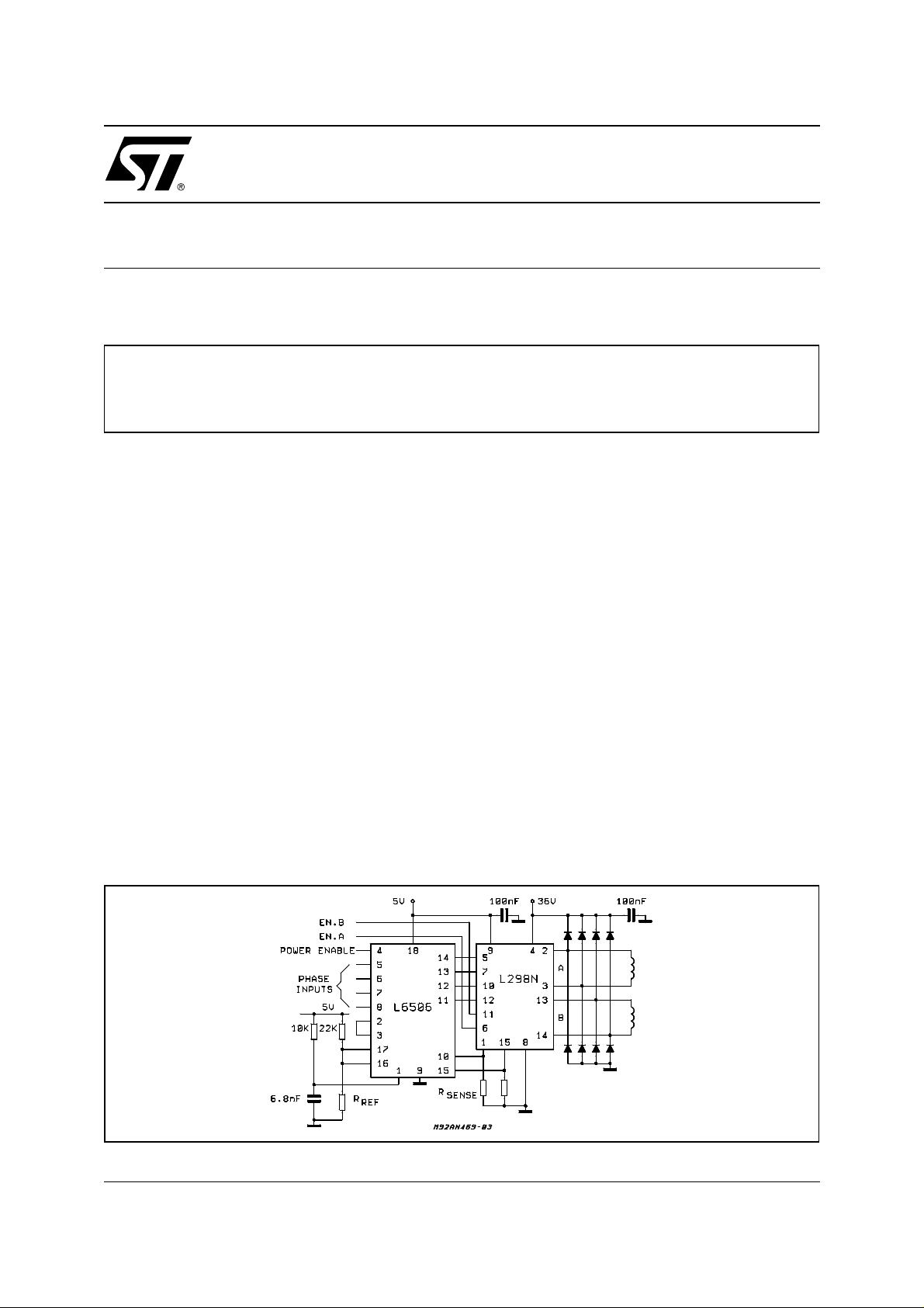
in figure 1 shows the L6506 used in conjunction with the L298N in a 2 phase bipolar stepper motor application.
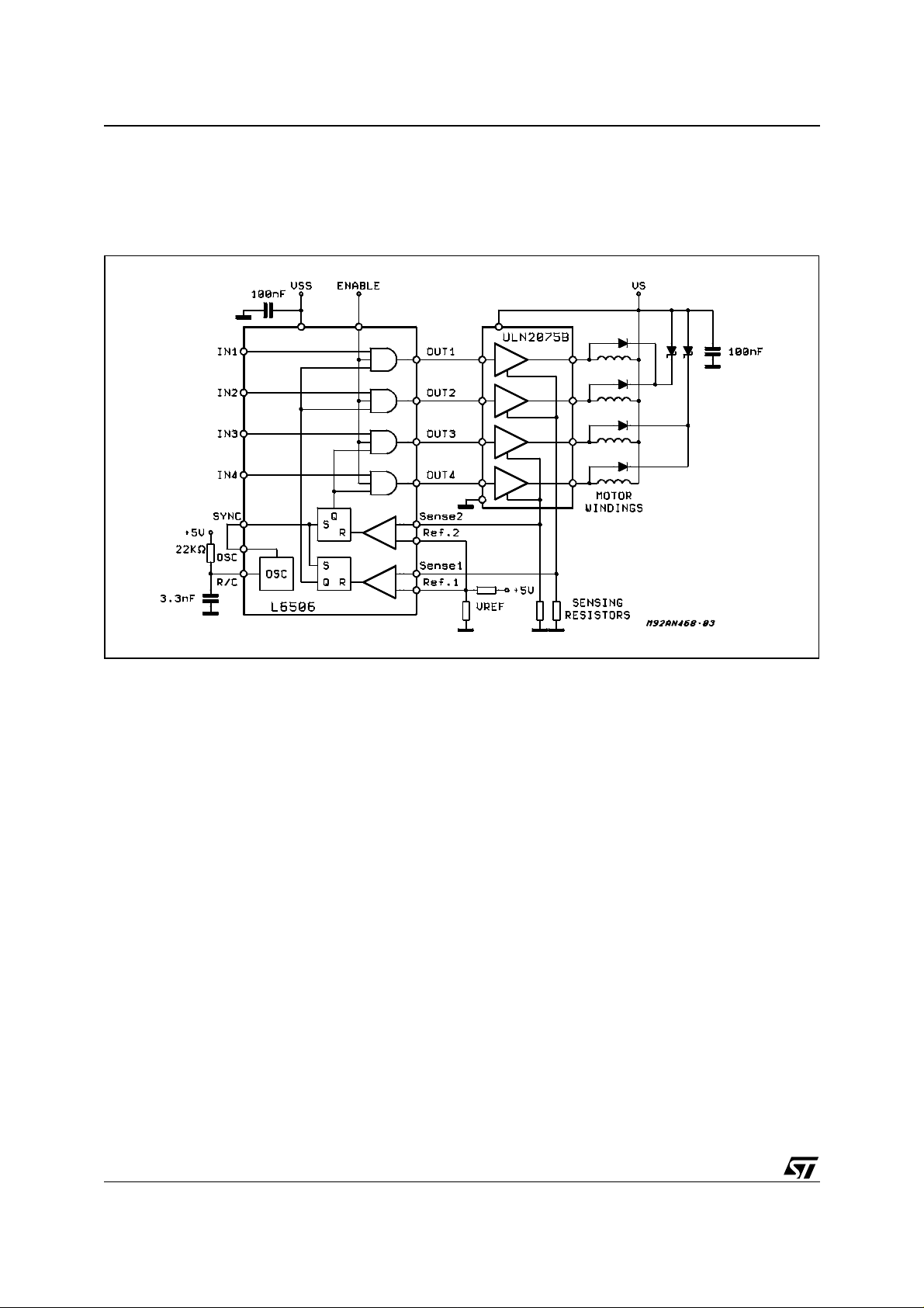
The circuit in figure 2 implements a similar 4 phase unipolar application.
CURRENT CONTROL LOGIC
In these two circuits, the L6506 is used to sense and control the current in each of the load windings. The current
is sensed by monitoring the voltage across a sense resistor (Rsense) and using a Pulse W idth M odulated control to maintain the current at the desired value.
An on -chip osc illator d rives the dual chopper and sets the operating frequency. An RC network on pin 1 sets the
operating frequency, which is given by the equation :
1
f
----------------------------=
0.69R1C1
for R1 > 1 0 K
Figure 1. Application Circuit for Bipolar 2 Phase Stepper Motor.
Ω
(1)
November 2003
1/6
Page 2
AN469 APPLICATION NO TE
The oscillator provides pulses to set the two flipflops, which in turn cause the outputs to activate the power actuator. Once the outputs have been activated the current in the load starts to increase, limited by the inductive
characteristic of the load.
Figure 2. Application Circuit for Unipolar 4 Phase Stepper Motor.
When the current in the load winding reaches the programmed peak value, the voltage across the sense resistor
(R
) is equal to reference voltage input (V
sense
) and the corresponding comparator resets its flip-flop. This in-
ref
terrupts the drive and allows the current to decay through a recirculating path until the next oscillator pulse occurs. The peak current in each winding is programmed by selecting the value of the sense resistor and Vref and
is given by the equation :
V
I
peak
ref
------------------=
(2)
R
sense
The minimum output pulse width is determined by the pulse width of the oscillator, or other signal applied to the
sync input. The internal oscillator is designed to provide narrow pulses to the sync input but the pulse width
should be considered carefully.
In some applications it is desirable to set the pul se width of this sync pulse to be just longer t han the turn on
delay time of the actuator stage. This may be useful in systems where the switching noise or recovery current
of the catch diodes, which passes through the sense resistor, causes the comparator to sense a current above
the peak current. By making the sync pulse wide enough to hold the flip-flop set at the time the switching transient occurs will cause the device to ignore this false data. When the internal oscillator is used the pulse width
can be modified by changing the value of the capacitor on pin 1.
Increasing the capacitance will widen the pulse width. The L6506 may be used with either a bridge driver, as
shown in figure 1, for bipolar motors or a quad darlington array, as shown in figure 2, for 4 phase unipolar motors. For eigher configuration, half step may be implemented using the 4 phase inputs with the input waveforms
shown in figure 3.
The recirculation path for the motor cur rent is through a c atc h diode for unipolar motors , or a c atch diode and
2/6
Page 3

AN469 APPLICATION NOTE
one of the lower transistors of the bridge for bipolar motors. Both of these implementations produce a low ripple
current since the voltage across the motor during the recirculation time is much less than the power supply voltage. Figure 4 shows the ripple current for bipolar motor applications using the L6506 and the L298N.
Figure 3. Input Signal for Stepper Motor Drive.
When implementing a half step drive, both outputs of the L6506 will be low during the half step of one phase.
This means a very long time is required for the current in the "off" winding to decay when driving bipolar motors.
Alternately, the power stage (L298N) may be inhibited to put the output in the state and achieve a faster current
decay. Since separate Vref inputs are provided for each channel, each of the loads may be programmed independently allowing the device to be used to implement microstepping or applications with different peak and
hold currents. In this type of application, changing the reference voltage (Vref) will change the load current, effectively implementing a transconductance amplifier.
SYNCHRONIZING MULTIPLE DEVICES
Ground noise problems in multiple configurations can be avoided by synchronizing the oscillators. This may be
done by connecting the sync pins of each of the devices with the oscillator output of the master device and connecting the R/C pin of the unused oscillators to ground as show n in figure 5.
The devices may be synchronized to external circuits by applying synchronizing pulses to the sync pins. It
should be noted, however, that the input pulse sets the minimum on time of the outputs and will ther efo re set a
minimum output average current.
Figure 4. Ripple Current in Bipolar Motors. Figure 5. Synchronizing Multiple Devices.
3/6
Page 4

AN469 APPLICATION NO TE
SYNCHRONIZING MULTIPLE DEVICES
Ground noise problems in multiple configurations can be avoided by synchronizing the oscillators. This may be
done by connecting the sync pins of each of the devices with the oscillator output of the master device and connecting the R/C pin of the unused oscillators to ground as show n in figure 5.
The devices may be synchronized to external circuits by applying synchronizing pulses to the sync pins. It
should be noted, however, that the input pulse sets the minimum on time of the outputs and will ther efo re set a
minimum output average current.
SELECTING THE OSCILLATOR COMPONENTS
When selecting the values for the external components for the oscillator one of the primary considerations is the
operating frequency. In addition there is another important consideration for these components.
In many applications the reverse recovery current of the free wheeling diodes and of parasitic elements in the
power stage will flo w through the sensing resistor in addition to the load current. Also there is sometimes noise
generated in the system when the power stage is swiched on. These two sources of error can fool the current
limiting stage and make it appear to operate at a subharmonic of the desired frequency. With the proper selection of the oscillator components this behavior can be avoided.
The design of the L6506 is such that the flip-flops used in the device are set dominant so that whenever the sync
input is low the Q output of the fl ip-fl op will be hi gh even if t he reset i s applied by the comparator at t he same
time. This characteristic of the flip-flops can be used to make the current sensing immune to the recovery currents and noise spikes that occur when t he power devices s witch. I f t he sync pul se i s l onger t han the turn on
delay time of the power stage, as shown in figure 6, these two sources of errors will be ignored.
To select the proper values for the oscillator components a more detailed equation for the operating frequency
and duty cycle of the oscillator is required.
The required equations can be derived from the equivalent circuit for the oscillator section sho w n in figure 7.
As can be seen from figure 7, the full equation for the operating frequency includes not only the external resistance and capacitance but the internal discharge resistor as well.
The full equation for the operating frequency is:
: (3)
------------------------------------------------------------------- -=
f
0.69C1 R1
1
R1 Ri⋅
+
--------------------
R1 Ri+
The equations for the active time of the sync pulse (T2), the i nactive t i me of the sync signal ( T1) and the duty
cycle can also be found by looking at the figure 7 and are :
T2 0.69C1
R1Ri
--------------------=
R1 Ri+
(4)
T1 = 0.69 R1 C1 (5)
T2
DC
-------------------- -=
T1 T2+
(6)
By substituting equations 4 and 5 into equation 6 and solving for the value of R1 the following equations for the
external components can be derived:
4/6
R1
1
-------- - 2–
DC
(7)
Ri=
Page 5

AN469 APPLICATION NOTE
T1
C1
------------------- -=
0.69R1
Looking at equation 4 it can easily be seen that the minimum pulse width of T2 will occu r when the value of Ri
is at its minimum and the value of R1 at its maximum.
(8)
Therefore, when evaluating equation 7 the minimum value for Ri of 700
Ω
(1 KΩ –30 %) should be us ed to guar-
antee the required pulse width.
For a typical application using the L298, which has a maximum turn on delay of 2.5
the following operating points:
f = 20 KHz
T1 + T2 = 50
T2 min = 3
µ
s
µ
s
From equation 6:
3µs
DC
------------- - 0.06==
50 µs
From equation 7:
1
R1
----------- 2
0.06
700 10.3KΩ==
From equation 8:
47 µs
------------------------------------- - 6.6nF==
C1
0.69()10.3 K()
µ
s, with the L6506 consider
Figure 6. Load Current and Sync Pulse. Figure 7. Oscillator Circuit and Waveforms.
5/6
Page 6

AN469 APPLICATION NO TE
Information furnished is believed to be accurate and reliable. However, STMicroelectronics assumes no responsibility for the consequences
of use of such information nor for any infringement of patents or other rights of third parties which may result from its use. No license is granted
by implic ation or otherwise under any patent or p atent right s of STMicroelectr oni cs. Spec i fications mentioned i n this publication are subje ct
to change without notice. This publication supersedes and replaces all information previously supplied. STMicroelectronics products are not
authorized for use as cri tical comp onents in life support dev i ces or systems wi thout express written approval of STMicroel ectronics.
The ST logo is a registered trademark of STMicroelectr oni cs.
All other n am es are the pro perty of thei r respectiv e owners
© 2003 STMi croelectro ni cs - All rights reserved
Australi a - B elgium - Brazil - Canada - China - Czech Republ i c - Finland - France - Germ any - Hong Kong - India - Is rael - Italy - Japan -
Malaysia - Malta - Morocco - Singapore - Spain - Sweden - Switzerland - United Kingdom - United States
STMicroelectronics GROUP OF COMPANIES
www.st.com
6/6
 Loading...