

Page 1
AN440
Application note
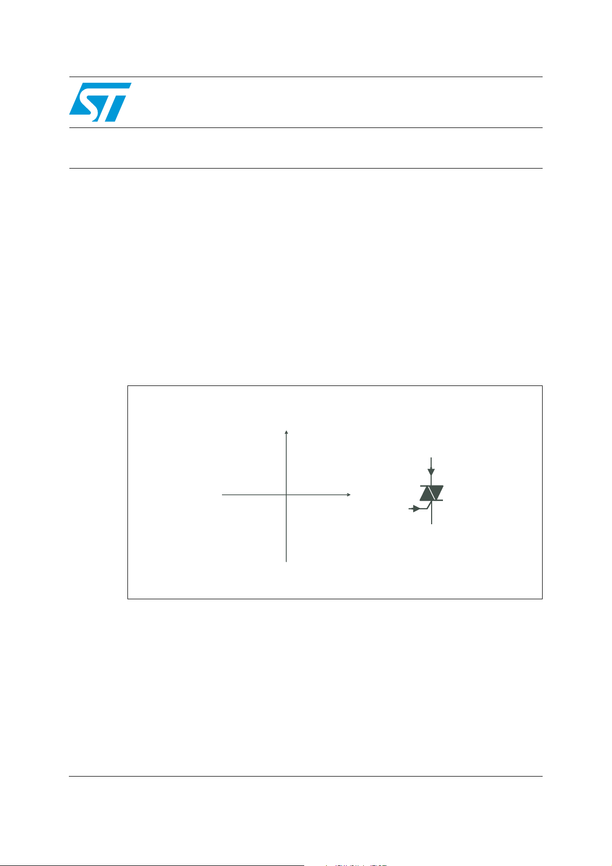
QII and QIII TRIAC triggering with positive power supply
Introduction
New TRIACs with high commutation and dv/dt performances are now available on the
market.
Generally these TRIACs can be triggered only in the first three quadrants (case of
Snubberless™, logic level and Snubberless high temperature TRIACs) as shown in
Figure 1.
This paper describes a trigger circuit supplying a negative gate current for quadrants II and
III implemented in a system using a positive power supply.
Without a new design, just by adding a capacitor and a diode, new series TRIACs can
replace conventional TRIACs.
Figure 1. The quadrants of Snubberless, logic-level, and Snubberless high
temperature TRIACs
I
I
T
T
+-
+-
nd
nd
2
2
rd
rd
3
3
--
--
+ +
+ +
st
st
1
1
th
th
4
4
NOT
NOT
TRIGGERABLE
TRIGGERABLE
I
I
G
G
TM: Snubberless is a trademark of STMicroelectronics
A
A
1
1
I
I
T
T
I
I
G
G
A
A
2
2
March 2008 Rev 3 1/8
www.st.com
Page 2
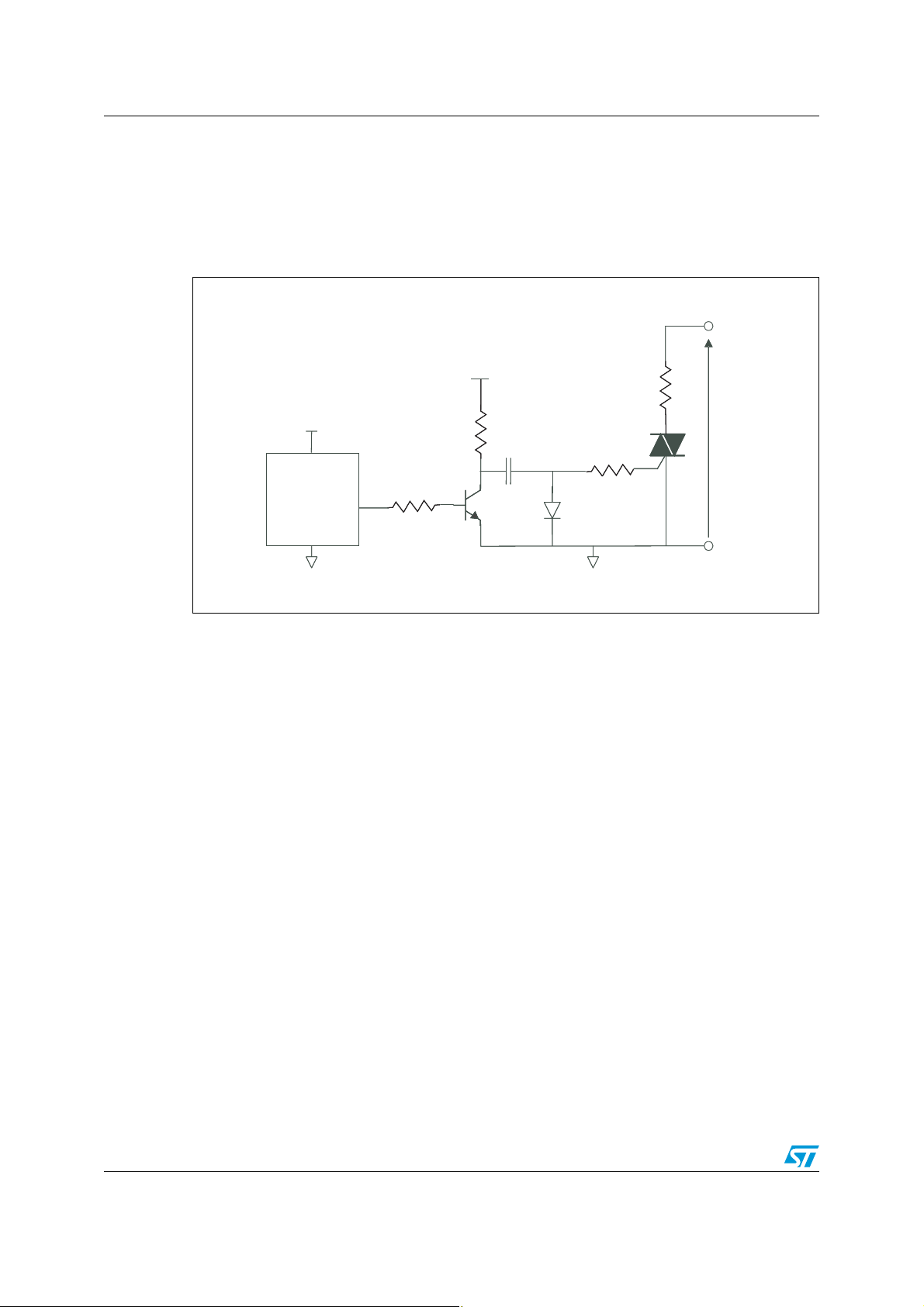
Principle of proposed gate circuit AN440
1 Principle of proposed gate circuit
To drive the TRIAC in the 2nd and 3rd quadrants, a discharge capacitor is used as shown in
Figure 2.
Figure 2. Basic diagram of the triggering circuit
+ Vcc
MCU
MCU
+ Vcc
+ Vcc
I/O
I/O
R3
R3
Tr
Tr
+ Vcc
R2
R2
C
C
D
D
LOAD
LOAD
R1
R1
TRIAC
TRIAC
LINE
GND
GND
GND
GND
When the transistor Tr is switched off, capacitor C is charged through resistance R2 and
diode D. The diode is used to avoid a capacitor charging current through the TRIAC gate. A
Schottky diode could be used to keep the voltage drop level below the gate non trigger
voltage (V
). When the TRIAC is triggered, Tr transistor is switched on, C is discharged
GD
through R1 and Tr and a negative current flows through the TRIAC gate.
We have to consider different parameters to define all the components:
● The TRIAC gate triggering current (I
● The time duration of the gate current pulse.
● The TRIAC latching current (I
) especially for low rms current loads.
L
GT
).
2/8
Page 3
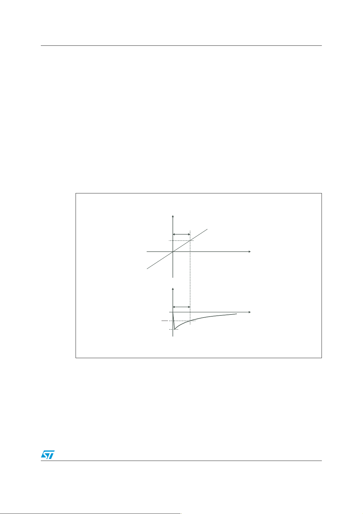
AN440 Gate current pulse width setting
2 Gate current pulse width setting
The TRIAC latching current (IL) is the minimum value of the main current which allows the
component to remain in the conducting state after the gate current I
That is to say the gate current has to be higher than I
until the main current reaches the
GT
latching current.
Example: for most of CW Snubberless TRIACs (refer to datasheet for further information):
has been removed.
G
Q1 – Q3: I
Q2: I
max = 50 mA
L
max = 60 mA
L
Example: for most BW Snubberless TRIACs:
Q1 – Q3: I
Q2: I
max = 70 mA
L
max = 80 mA
L
Figure 3. Gate control principle
I
I
a1
a1
t
t
1
1
I
I
Lmax
Lmax
I
I
g
g
t
t
1
1
t
t
t
I
I
GM
GM
2
2
I
I
GM
GM
t
3/8
Page 4

Gate current pulse width setting AN440
t1 calculation
The TRIAC gate has to be supplied to reach an anode current higher than the latching
current. Furthermore, a minimum gate current pulse width of 20 µs has to be ensured. The
minimum t
t
Where ω = 2.π.f and f is mains frequency.
I
RMS
Figure 4 shows the minimum time versus I
level is then given by the following equation:
1
MAX
·
⎞
⎟
+
20 µs
⎟
2I
⎠
⎛
⎜
⎜
⎝
I
L
RMS
1
≥
asin
1
ω
: minimum rms current of the load (depending on line and load variations).
load current for a 50Hz application.
RMS
Figure 4. t
time versus I
1
200
180
160
140
120
100
80
60
40
20
0
Note: Curve given for V
I
is the maximum gate trigger current specified in the data sheet. To ensure a good safety
GT
margin and a good triggering we chose I
The gate resistor can be defined by the following equation:
R--=
CC
1
for different load currents (worst case: ILQ2)
RMS
t1 (µs)
t1 (CW -> 60mA)
t1 (BW -> 80mA)
BW SERIES
CW SERIES
01234567891011121314151617181920
IT(rms) (A)
= 1 V and V
CE
VVV
I
GM
CEGK
GK
= 1.3 V
GM
= 2.IGT.
with typically V
= 1 V and VGK = 1.3 V at IGM = 2.I
CE
Capacitor C is then given by the following equation (where t1 is given by Figure 4):
t
C
1
≥
()
2·lnR
1
Figure 5 gives the minimum capacitance versus supply voltage for different TRIACs series.
To ensure that capacitor C will be charged for the nest half cycle, R
this equation (charging time constant < 1 ms):
0.001
R2<
4/8
C
GT
could be chosen with
2
Page 5

AN440 Gate current pulse width setting
Figure 5. Capacitance value versus supply voltage for different sensitivities
C (µF)
3
2.8
2.6
2.4
2.2
2
1.8
1.6
1.4
1.2
1
0.8
0.6
CW SERIES
0.4
0.2
0
0 2 4 6 8 1012141618202224262830
BW SERIES
Vcc (V)
C (CW -> 60mA)
C (BW -> 80mA)
5/8
Page 6

Experimental results AN440
3 Experimental results
Figure 6 gives a typical oscillogram within the following conditions:
● TRIAC = BTA08-600CW
● I
● Line voltage: 230 V rms, 50 Hz
● V
● R
● R
● C = 3.3 µF
Figure 6. Triggering at zero current
= 2.12 A (load power: 500 W)
RMS
= 5 V
CC
= 36 Ω
1
= 300 Ω
2
Anode
Anode current
(500 mA/div)
div)
Gatecurrent
Gate current
div)
(50 mA/div)
The component values are given in the following table for different application cases.
Table 1. Component values for 3 different cases. TRIAC: BTA08-600CW
(I
= 35 mA)
GT
I
= 2 A
RMS
= 5 V
V
cc
(µs) 87.5 47 47
t
1MIN
R
(Ω) 39 39 110
1MAX
C
(µF) 3.3 1.76 0.62
MIN
R
(Ω) 306 569 1622
2MAX
I
RMS
V
cc
= 5 A
= 5 V
I
RMS
V
cc
= 5 A
= 10 V
6/8
Page 7

AN440 Conclusion
4 Conclusion
In the case of controllers supplied by positive voltage this solution allows the replacement of
conventional TRIACs used in the 1st and 4th quadrants by Snubberless or LOGIC LEVEL
TRIACs which operate only in the first three quadrants. This solution only requires the
addition of a capacitor and a diode to control each TRIAC.
With inductive loads (motor, transformer, etc...) a pulse train can be used because of the
phase lag between current and voltage.
In the case of logic or transistor failure, the capacitor C operates as an open circuit for dc
current and avoids all triggering. This factor acts as a safety feature.
But this trigger circuit can not be effectively used to drive small loads (like valves, fan etc...)
because the latching current value is quite high compared to the load current. In this case a
dc gate current is required.
Then the V
point of the power supply should be connected to A1 to sink the current
CC
directly from the gate with the control circuit. There is then no need of a supplementary
capacitor and diode. This solution is then easier and cheaper.
5 Revision history
Table 2. Document revision history
Date Revision Changes
May-1992 1 Initial release.
23-Apr-2004 2 Style sheet update. No Content change.
10-Mar-2008 3 Reformatted to current standards. Full technical review
7/8
Page 8

AN440
Please Read Carefully:
Information in this document is provided solely in connection with ST products. STMicroelectronics NV and its subsidiaries (“ST”) reserve the
right to make changes, corrections, modifications or improvements, to this document, and the products and services described herein at any
time, without notice.
All ST products are sold pursuant to ST’s terms and conditions of sale.
Purchasers are solely responsible for the choice, selection and use of the ST products and services described herein, and ST assumes no
liability whatsoever relating to the choice, selection or use of the ST products and services described herein.
No license, express or implied, by estoppel or otherwise, to any intellectual property rights is granted under this document. If any part of this
document refers to any third party products or services it shall not be deemed a license grant by ST for the use of such third party products
or services, or any intellectual property contained therein or considered as a warranty covering the use in any manner whatsoever of such
third party products or services or any intellectual property contained therein.
UNLESS OTHERWISE SET FORTH IN ST’S TERMS AND CONDITIONS OF SALE ST DISCLAIMS ANY EXPRESS OR IMPLIED
WARRANTY WITH RESPECT TO THE USE AND/OR SALE OF ST PRODUCTS INCLUDING WITHOUT LIMITATION IMPLIED
WARRANTIES OF MERCHANTABILITY, FITNESS FOR A PARTICULAR PURPOSE (AND THEIR EQUIVALENTS UNDER THE LAWS
OF ANY JURISDICTION), OR INFRINGEMENT OF ANY PATENT, COPYRIGHT OR OTHER INTELLECTUAL PROPERTY RIGHT.
UNLESS EXPRESSLY APPROVED IN WRITING BY AN AUTHORIZED ST REPRESENTATIVE, ST PRODUCTS ARE NOT
RECOMMENDED, AUTHORIZED OR WARRANTED FOR USE IN MILITARY, AIR CRAFT, SPACE, LIFE SAVING, OR LIFE SUSTAINING
APPLICATIONS, NOR IN PRODUCTS OR SYSTEMS WHERE FAILURE OR MALFUNCTION MAY RESULT IN PERSONAL INJURY,
DEATH, OR SEVERE PROPERTY OR ENVIRONMENTAL DAMAGE. ST PRODUCTS WHICH ARE NOT SPECIFIED AS "AUTOMOTIVE
GRADE" MAY ONLY BE USED IN AUTOMOTIVE APPLICATIONS AT USER’S OWN RISK.
Resale of ST products with provisions different from the statements and/or technical features set forth in this document shall immediately void
any warranty granted by ST for the ST product or service described herein and shall not create or extend in any manner whatsoever, any
liability of ST.
ST and the ST logo are trademarks or registered trademarks of ST in various countries.
Information in this document supersedes and replaces all information previously supplied.
The ST logo is a registered trademark of STMicroelectronics. All other names are the property of their respective owners.
© 2008 STMicroelectronics - All rights reserved
STMicroelectronics group of companies
Australia - Belgium - Brazil - Canada - China - Czech Republic - Finland - France - Germany - Hong Kong - India - Israel - Italy - Japan -
Malaysia - Malta - Morocco - Singapore - Spain - Sweden - Switzerland - United Kingdom - United States of America
www.st.com
8/8
 Loading...