


AN437
Application note
RC snubber circuit design for TRIACs
Introduction
When a TRIAC controls inductive loads, the mains voltage and the load current are not in
phase. To limit the slope of the reapplied voltage and ensure right TRIAC turn-off, designer
usually used a snubber circuit connected in parallel with the TRIAC. This circuit can also be
used to improve TRIAC immunity to fast transient voltages.
The subject of this paper is, first of all, to analyze the snubber circuit functions and to
propose a method for snubber circuit design in order to improve turn-off commutation.
Contents
1 Snubber circuit functions and drawback . . . . . . . . . . . . . . . . . . . . . . . . 2
1.1 Turn-off improvement . . . . . . . . . . . . . . . . . . . . . . . . . . . . . . . . . . . . . . . . . 2
1.1.1 TRIAC turn-off reminder . . . . . . . . . . . . . . . . . . . . . . . . . . . . . . . . . . . . . 2
1.1.2 Snubber circuit benefit at TRIAC turn-off . . . . . . . . . . . . . . . . . . . . . . . . . 3
1.2 Overvoltage limitation at turn-off . . . . . . . . . . . . . . . . . . . . . . . . . . . . . . . . 4
1.3 Immunity to fast voltage transient improvement . . . . . . . . . . . . . . . . . . . . . 5
1.4 Turn-on stress due to snubber circuit discharge . . . . . . . . . . . . . . . . . . . . . 5
2 How to design snubber circuit for turn-off improvement . . . . . . . . . . . 7
2.1 Step response of an RLC series circuit . . . . . . . . . . . . . . . . . . . . . . . . . . . 7
2.2 RC snubber circuit design . . . . . . . . . . . . . . . . . . . . . . . . . . . . . . . . . . . . . 9
2.2.1 Is the snubber circuit required? . . . . . . . . . . . . . . . . . . . . . . . . . . . . . . . . 9
2.2.2 Resistor and capacitor snubber circuit design . . . . . . . . . . . . . . . . . . . . 10
3 Conclusion . . . . . . . . . . . . . . . . . . . . . . . . . . . . . . . . . . . . . . . . . . . . . . . . 14
Appendix A RLC series circuit step response explanation . . . . . . . . . . . . . . . . 15
Revision history . . . . . . . . . . . . . . . . . . . . . . . . . . . . . . . . . . . . . . . . . . . . . . . . . . . . 17
October 2007 Rev 2 1/18
www.st.com
Snubber circuit functions and drawback AN437
1 Snubber circuit functions and drawback
1.1 Turn-off improvement
1.1.1 TRIAC turn-off reminder
When a TRIAC switches from on-state to off-state, the current passes through zero and the
supply voltage is reapplied instantaneously across the structure. In certain conditions, the
component is not able to block this voltage and then turns on spontaneously.
Indeed, a TRIAC can be compared to two Thyristors mounted in back-to-back and coupled
with a single control area. To trigger the two Thyristors, the control area overlaps the two
conduction areas.
During the conduction time, a certain quantity of charges is injected into the structure.
These charges disappear by recombination during the current decrease and by extraction
after the turn-off with the reverse recovery current (refer to Figure 1). Nonetheless, an
excess of charge remains, particularly in the neighboring regions of the gate, which can
induce the triggering of the other conduction area when the mains voltage is reapplied
across the TRIAC (refer to Figure 2).
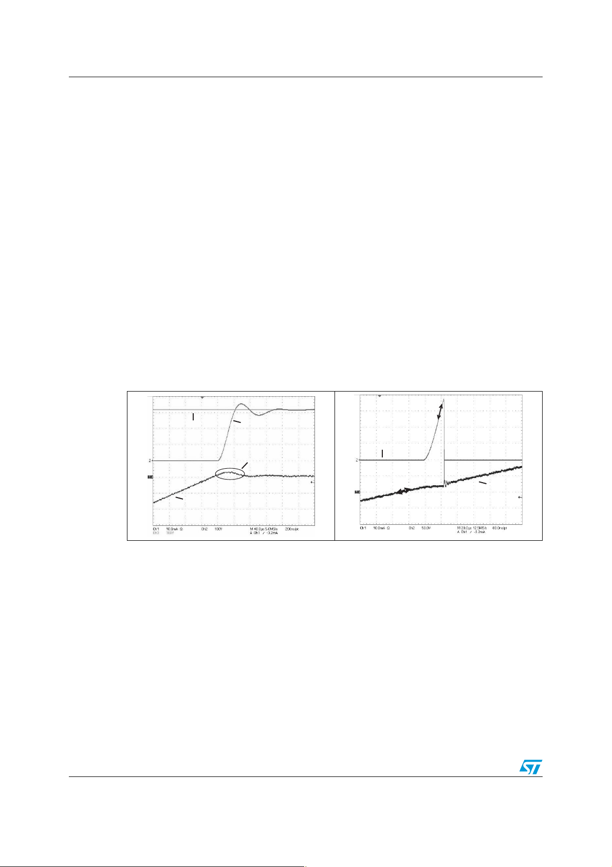
Figure 1. TRIAC turn-off on inductive
load - suitable turn-off
V
Mains
(100 V/div)
IT(10 mA/div)
VT(100 V/div)
Recovery current
Figure 2. TRIAC turn-off on inductive
load - spurious triggering
dV/dt
OFF
VT(50 V/div)
IT(10 mA/div)
dI/dt
OFF
A spurious triggering depends on:
● The slope of the decreasing current, called the turn-off dI/dt or dI/dt
. This parameter
OFF
determines the quantity of charges which remains, when the current drops to zero, and
which could be injected in the gate area or in the opposite Thyristor.
● The slope of the reapplied voltage, called the turn-off dV/dt or dV/dt
. This parameter
OFF
defines the capacitive current which could be injected through the gate.
2/18
AN437 Snubber circuit functions and drawback
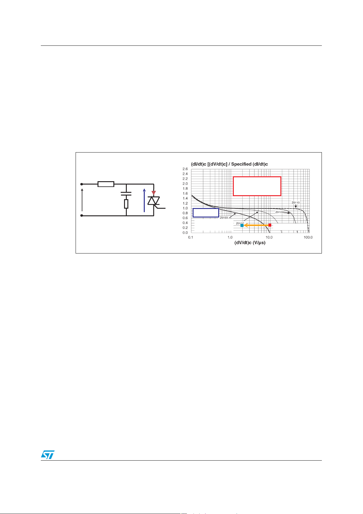
1.1.2 Snubber circuit benefit at TRIAC turn-off
The TRIAC turn-off behavior is characterized by the datasheet curve between the critical
rate of decrease of commutating on-state current ((dI/dt)c) and the critical rate of rise of
commutation off-state voltage ((dV/dt)c) (refer to Figure 3). These parameters are specified
for the maximum operating junction temperature (worst case).
In practice, the current waveform, and thus the slope of the decreasing current, is imposed
by the load. The user can then only limit the slope of the reapplied voltage. Indeed, by
adding an snubber circuit across the TRIAC, the circuit time response is increased and thus,
dV/dt
Figure 3. (dI/dt)c versus (dV/dt)c curve for Z01 standard TRIACs and snubber
is decreased (refer to Figure 3).
OFF
circuit impact
Load
I
C
V
Mains
V
R
T
T
Safe area
Operating point
with RC snubber
Area of spurious
firing at
commutation
Operating point
An RC snubber circuit must be used when there is a risk of TRIAC spurious triggering, i.e.
when the dI/dt
OFF
-dV/dt
couple, measured in the application, is higher than the TRIAC
OFF
datasheet values, (dI/dt)c at a given (dV/dt)c.
Figure 4 shows the turn-off behavior of a Z0103 standard TRIAC which controls a 26 W
drain pump. Without snubber circuit and for the maximum junction temperature (110° C), a
spurious triggering appears at turn-off. Indeed, the measured (dI/dt)
and (dV/dt)
OFF
OFF
values, equal respectively to 0.13 A/ms and 10 V/µs, are higher than the guarantee (dI/dt)c (dV/dt)c point (only 7 V/µs @ 0.13 A/ms, see Figure 3).
Thanks to an RC snubber circuit (10 nF and 2.7 kΩ), the slope of the reapplied voltage can
be limited to 1.5 V/µs and thus spurious triggering at turn-off can be avoided (see Figure 3
and Figure 4).
3/18
Snubber circuit functions and drawback AN437
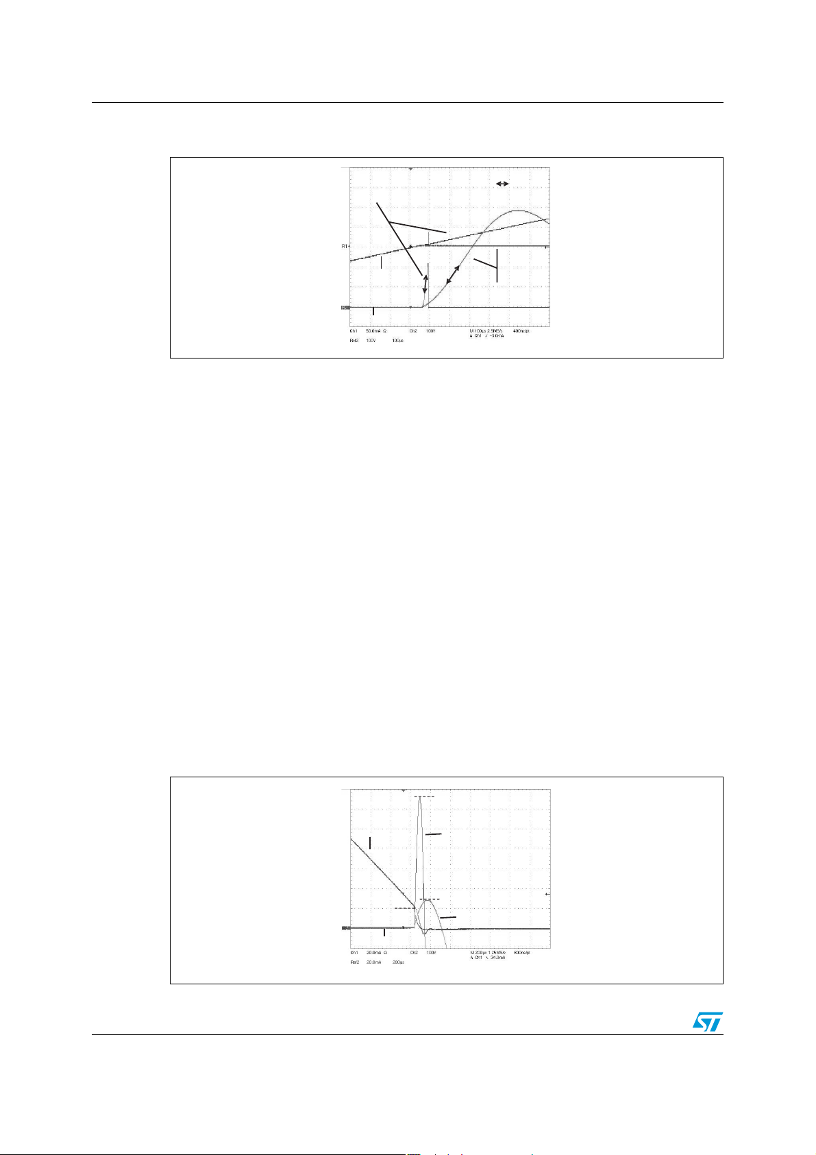
Figure 4. Z0103 TRIAC turn-off on inductive load without and with snubber circuit
(C = 10 nF and R = 2.7 kΩ)
:dV/dt
Without
IT(50 mA/div)
VT(100 V/div)
snubber
With
OFF
snubber
The snubber circuit design, detailed in Section 2: How to design snubber circuit for turn-off
improvement, is a trade-off between the maximum peak off-state voltage under pulse
conditions (V
DSM
/ V
), the critical slope of reapplied voltage ((dV/dt)c) and the turn-on
RSM
stress (dI/dt). When low load inductances are controlled or, low damping factor or low slope
of reapplied voltage are considered, the snubber circuit design can lead to choose a low
snubber resistance value. To reduce the snubber capacitance discharge at turn-on, the
resistance value is limited to a minimum value (refer to Section 1.4).
1.2 Overvoltage limitation at turn-off
When a TRIAC controls low root-mean-square currents inductive loads, an overvoltage
could occur when the current reaches the holding current (I
If the maximum value of the overvoltage (V
under pulse conditions (V
DSM
/ V
), the TRIAC may conduct without any gate current or
RSM
may be even damaged. The protections against overvoltage at turn-off are:
● A clamping strategy - use a varistor or an ACSTM / ACST (refer to AN1172 about
protected AC Switch™).
● A damping strategy - a snubber circuit. An RC snubber circuit limits the slope of the
voltage rise and could maintain the overvoltage at a lower value than the maximum
allowed value.
Figure 5. Overvoltage at TRIAC turn-off with and without snubber circuit
(C = 10 nF and R = 2.7 kΩ)
IT(20 mA/div)
I
H
) exceeds the maximum peak off-state voltage
M
VM= 660 V
Without snubber
VM= 140 V
With snubber
) (refer to Figure 5).
H
VT(100 V/div)
4/18

AN437 Snubber circuit functions and drawback
1.3 Immunity to fast voltage transient improvement
Electrical noise may appear on the mains and generates across the TRIAC fast voltage
variations, as described in IEC 61000-4-4 standard.
Fast voltage variations can create a gate current (I
), due to the junction capacitance
G
between A2 and the gate, and could trigger the TRIAC. The maximum rate of rise of offstate voltage that a TRIAC is able to withstand without turning on is called the static dV/dt. A
spurious triggering due to static dV/dt is not dangerous for a component. The aim of the
snubber circuit is to reduce the static dV/dt at a lower level than the dV/dt specified in the
datasheet to avoid spurious triggering.
An RC snubber circuit improves the TRIAC immunity against fast voltage transients. For
example, regarding to the standard IEC 61000-4-4, a Z0109 standard TRIAC has a typical
immunity level of about 0.7 kV, without any snubber circuit. With a snubber circuit (1 nF and
47 Ω), the Z0109 immunity level can reach 4.0 kV.
Designers must manage the following trade-off to choose the suitable RC snubber circuit:
● Reduce dV/dt rates: the snubber capacitance must be high and the snubber resistance
must be low;
● Reduce dI/dt rate at turn-on (refer to Section 1.4): the snubber capacitance must be low
and the snubber resistance must be high.
1.4 Turn-on stress due to snubber circuit discharge
The snubber circuit design can lead to low resistance value. However, the snubber resistor
reduces the rate of current rise at turn-on (dI/dt
dI/dt
than the dI/dt specified in the datasheet may damage the TRIAC.
ON
The rate of current rise is directly proportional to the initial capacitance voltage and inversely
proportional to the series inductances of the board and the snubber resistor. The rate of
current rise depends also on the turn-on speed of the TRIAC, the triggering quadrants and
the gate current amplitude. So, there is no simple way to predict the rate of current rise.
) during the capacitor discharge. An higher
ON
Usually, the inductance of the circuit layout is very low, in the range of few nH. Indeed, to
optimize the snubber circuit efficiency, the snubber circuit must be located very close to the
TRIAC (tracks length lower than 2 cm).
From datasheet specifications, there are three ranges of maximum dI/dt:
● dI/dt = 20 A/µs: for low current rating of TRIACs (0.8 A and 1 A).
● dI/dt = 50 A/µs: for the other TRIACs (4 A up to 40 A).
● dI/dt = 100 A/µs: for some ACSTs (6 A up to 12 A).
To keep the dI/dt
below 50 A/µs for TRIACs and below 100 A/µs for ACSTs, the snubber
ON
resistance must be typically higher than 47 Ω (refer to Figure 6). For a 20 A/µs maximum
dI/dt, the minimum resistance value is about 620 Ω. Therefore, depending on the component
used, some tests should be performed to define accurately the minimum resistance value.
5/18
Snubber circuit functions and drawback AN437
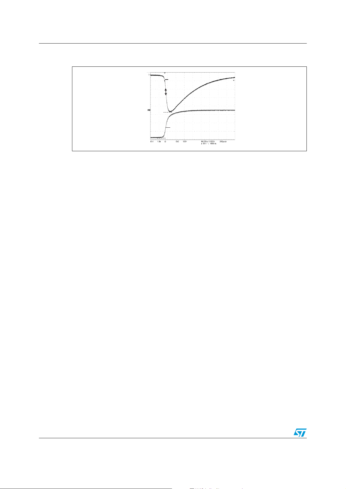
Figure 6. Typical snubber circuit discharge (C = 10 nF and R = 47 Ω) with
BTA/BTB16 TRIAC at peak mains voltage (quadrant 3, I
IT(1 A/div)
dI/dtON=50A/µs
I
Max.
VT(100 V/div)
V
= 320 V
Max.
= 2 x IGT)
G
6/18

AN437 How to design snubber circuit for turn-off improvement
2 How to design snubber circuit for turn-off
improvement
2.1 Step response of an RLC series circuit
The RSCS snubber circuit makes up a resonant circuit with an inductive load (refer L and R
on Figure 7). At turn-off, the snubber circuit limits the slope of the reapplied voltage
(dV/dt
off to respect both the reapplied voltage slope ((dV/dt)c) and the maximum peak off-state
voltage under pulse conditions (V
The electrical circuit analyzed in this paragraph is given by Figure 7.
Figure 7. Application circuit and its equivalent diagram at turn-off
) but generates an overvoltage (VP). The snubber circuit design results in a trade-
OFF
DSM
/ V
RSM
).
V
Mains
Application circuit
Load
LR
I
G
G
I
T
R
V
T
S
C
S
≈
E
VV
Cs Cs
Equivalent diagram at turn-off
Load
LR
I
T
V
T
For a second order linear differential equation with a step function input, the voltage
variation across the snubber capacitance (V
(t)) and the TRIAC (VT(t)) is given by:
Cs
Equation 1
2
1
·
2
ω
0
)t(Vd
.
ξ
Cs
2
dt
2
ω
0
)t(dV
Cs
dt
Cs
E)t(V
=++·
Equation 2
)t(dV
CR)t(V
Cs
SST
+··=
dt
)t(V
Cs
With damping factor:
Equation 3
R
S
C
S
+
=ξ
2
C
)RR(
)(S
Ω
)F(S
·
L
)H(
Undamped natural resonance:
Equation 4
=ω
)s/rad(0
CL1·
)F(S)H(
7/18

How to design snubber circuit for turn-off improvement AN437
Final voltage value:
Equation 5
L
ω
RMS
with
)sin(V2E
ϕ··=
)sin(
ϕ
=
: mains rms voltage
V
RMS
·
22
)L(R
ω
·+
Snubber circuit divider ratio:
Equation 6
R
S
=
M
By solving the second order linear differential equation according to the damping factor and
initial conditions (refer to Appendix A: RLC series circuit step response explanation), two
diagrams can be defined. These diagrams give the slope of the voltage rise (dV/dt
the peak voltage (V
to Figure 8).
RR
+
S
) and
) according to the damping factor (ξ) and the load resistance (M) (refer
P
OFF
The voltage rise slope (dV/dt
) is defined as the maximum instantaneous voltage rise
OFF
slope.
Figure 8. Trade-off between normalized peak voltage (Z = VP/E), normalized voltage
rise slope (K = dV/dt
/(E x ω0)) according to damping factor (ξ) and the
OFF
divider ratio (M)
Z = V /E
P
2
1.9
1.8
1.7
1.6
1.5
1.4
1.3
1.2
1.1
1
0 0.2 0.4 0.6 0.8 1 1.2 1.4 1.6 1.8 2
K = dV/dt /(E x )
2.2
2
1.8
1.6
1.4
1.2
1
0.8
0.6
M decreases
0.4
0.2
0
0 0.2 0.4 0.6 0.8 1 1.2 1.4 1.6 1.8 2
M decreases
OFF
ω
Damping factor:
Damping factor:
0
ξ
ξ
M = 1
M = 0.75
M = 0.5
M = 0.25
M = 0
M=1
M = 0.75
M = 0.5
M = 0.25
M=0
As shown on these two diagrams, the load resistance (R) helps to reduce dV/dt
The load impact is significant if the damping factor is higher than 0.2.
8/18
OFF
and VP.

AN437 How to design snubber circuit for turn-off improvement
2.2 RC snubber circuit design
2.2.1 Is the snubber circuit required?
Without snubber circuit, the slope of reapplied voltage is limited by the TRIAC capacitance
between anode and cathode junction. The oscillating circuit is constituted by the load, L and
R, and the internal capacitance, C
For example, the typical internal capacitances of 1 A, 12 A and 24 A TRIACs are
respectively 12 pF, 90 pF and 180 pF (without direct voltage junction polarisation, worst
case). Without snubber circuit and for most part of inductive loads, the damping factor (ξ) is
generally lower than 1.
For an underdamped oscillating circuit (0 ≤ ξ < 1), the voltage variation across the TRIAC
(V
(t)) is:
T
Equation 7
⎛
⎜
⎜
⎝
With damped natural resonance:
+=
·-
ω
pT
, of the TRIAC.
T
·
ωξ
0
ω
p
⎞
t
··-
ωξ
0
⎟
e)tsin()tcos(·EE)t(V
.··
ω
p
⎟
⎠
Equation 8
2
1 ξωω -.=
0p
For example, in the case of a 26 W drain pump (L = 2.4 H and R = 190 Ω at 50 Hz)
controlled by a Z0103 TRIAC (C
4
).
= 12 pF), the damping factor is close to zero (ξ = 2.1 x 10
T
For low damping factor, the normalized voltage rise slope K is equal to 1 (refer to Figure 8,
lower graph). The maximum slope of reapplied voltage across the TRIAC is then:
Equation 9
C·L
· ϕ
)V(RMS
)F(T)H(
)sin(V2
6
-
10·
is equal to 59 V/µs without snubber circuit.
OFF
is in fact about 10 V/µs.
OFF
is always lower than the
OFF
·
dt/dV
=
µ
)s/V(OFF
According to this formula, the estimated dV/dt
As shown in Figure 9, the measured dV/dt
The error between the Equation 9 result and real value is due to the fact that we didn’t take
into account the load inductance saturation (real value is higher at low current), the parallel
parasitic capacitor of the load, the recovery current and the load resistance increase with
frequency. Moreover, the turn-off measurement is done with a voltage probe which adds a
12 pF capacitor across the TRIAC. So, the measured dV/dt
theoretical value, given by Equation 9.
-
9/18

How to design snubber circuit for turn-off improvement AN437
Figure 9. Z0103 TRIAC turn-off on inductive load (26 W drain pump) without
snubber circuit and in transient operating
V
(100 V/div)
V
(100 V/div)
Mains
Mains
VT(100 V/div)
VT(100 V/div)
IT(10 mA/div)
IT(10 mA/div)
dI/dt
dI/dt
OFF
OFF
VP= 350 V
VP= 350 V
dV/dt
= 10 V/µs
dV/dt
= 10 V/µs
OFF
OFF
= 0.13 A/ms
= 0.13 A/ms
An RC snubber circuit must be used when there is a risk of TRIAC spurious triggering, i.e.
when the measured dI/dt
and dV/dt
OFF
values are higher than the specified (dI/dt)c and
OFF
(dV/dt)c values.
In our application case and for the worst case load conditions (transient operating), the
measured (dI/dt)
and (dV/dt)
OFF
values are equal respectively to 0.13 A/ms and 10 V/µs.
OFF
These values are higher than the specified (dI/dt)c and (dV/dt)c values, see Section 1.1.2.
Thanks to an RC snubber circuit, rated in the next paragraph, the slope of the reapplied
voltage could be limited and thus spurious triggering at turn-off could be avoided.
2.2.2 Resistor and capacitor snubber circuit design
The snubber circuit design depends on the damping factor (ξ).
When ξ decreases, the snubber resistor and capacitor values decrease but the peak voltage
and snubber circuit discharge current increase. Maximum instantaneous dV/dt
a time later than t = 0 when ξ is lower than 0.5.
When ξ increases, the snubber resistor and capacitor values increase and the voltage
overshoot decreases. The maximum instantaneous dV/dt
higher than 0.5.
Low damping factors are recommended. Indeed, thanks to the high voltage capability of
TRIACs, the snubber circuit can be optimized to reduce the capacitor value and, in the same
way, reduce the snubber circuit cost.
To illustrate the RC snubber circuit design, a 26 W drain pump (L = 2.4 H and R = 190 Ω at
50 Hz) controlled by a Z0103 TRIAC is considered.
Two methods can be used to design the snubber circuit. The first method designs the RC
snubber circuit with load resistance consideration. The second method considers pure
inductive load.
The first method of RC snubber circuit design is divided in four steps:
1. Snubber resistance choice
OFF
occurs at
OFF
occurs at t = 0 when ξ is
To limit the TRIAC turn-on stress and optimize the TRIAC immunity against fast voltage
transients, the snubber resistance is fixed to the minimum value.
For Z01 TRIAC, the dI/dt at turn-on is limited to 20 A/µs. The minimum snubber resistance
value is 620 Ω (refer to Section 1.4).
10/18

AN437 How to design snubber circuit for turn-off improvement
Using Equation 6, the snubber circuit divider ratio M is equal to:
M = 0.77 with R = 190 Ω and R
= 620 Ω
S
2. Damping factor definition
The snubber capacitor depends on the undamped natural resonance (ω
) and the damping
0
factor (ξ). Consider the following modified forms of Equation 4 and Equation 3:
Equation 4 modified
1
C
S
with
2
L
·=ω
0
0
Where K is the normalized voltage rise slope (refer to the lower graphic in Figure 8).
dt/dV
=ω
OFF
KE
·
Equation 3 modified
S
+
L
4C ξ·
·=
From the two previous equations, the ratio between the normalized voltage rise slope (K)
and the damping factor (ξ) is given by Equation 10. Figure 10, derived from the lower graph
in Figure 8 gives the variation of this ratio with ξ:
2
2
)RR(
S
Equation 10
K
ξ
L
·=
2
+
RR
S
For the drain pump controlled (L = 2.4 H and R = 190 Ω at 50 Hz) and by using Equation 5,
the final voltage value E is:
E = 306 V for V
To avoid spurious triggering with Z0103 TRIAC, the dV/dt
maximum allowed (dV/dt)c, see Figure 2).
dt/dV
·
OFF
E
= 230 V and with ϕ ≈ 76°
RMS
is fixed to 2 V/µs (lower than
OFF
Thus according to Equation 10, the ratio between the normalized voltage rise slope and the
damping factor is equal to 38. Figure 10 gives then the damping factor value (ξ = 0.026).
Figure 10. Ratio between normalized voltage rise slope (K = dV/dt
/ (E x ω0)) and
OFF
damping factor (ξ) according to the damping factor (ξ)
K / ξ
100
38
10
M decreases
M decreases
1
0.1
ξ = 0.026
0.01 0.1 1 10
Damping factor: ξ
M = 1
M = 1
M = 0.75
M = 0.75
M = 0.5
M = 0.5
M = 0.25
M = 0.25
M = 0
M = 0
11/18

How to design snubber circuit for turn-off improvement AN437
3. Snubber capacitance and overvoltage calculations
The snubber capacitance is given by the modified form of Equation 3:
4C x· ·10
S(nF)
·=
L
2
)RR(
+
S
9
2
9.9 nF with = 0.026»x
The peak voltage is given in the upper graphic of Figure 8. A component with a 600 V
capability will be suitable.
V
= 1.92 · E ≈ 607 V with ξ = 0.026.
P
4. RC snubber circuit validation
The turn-off and turn-on behaviors must be checked experimentally to validate the designed
RC snubber circuit.
For turn-off commutation, the measured slope of the voltage rise is 1.7 V/µs (Figure 10) and
is very close to the theoretical slope (2 V/µs). The measured peak voltage (520 V) is lower
than the calculated value (607 V) due to the RLC model approximations (refer to
Section 2.2.1).
Figure 11. Z0103 TRIAC turn-off on inductive load with snubber circuit
(C = 10 nF and R = 620 Ω)
IT(10 mA/div)
IT(10 mA/div)
dI/dt
OFF
VP= 520 V
dV/dt
= 1.7 V/µs
V
V
Mains
Mains
(100 V/div)
(100 V/div)
OFF
VT(100 V/div)
VT(100 V/div)
The second method of RC snubber circuit design allows a quicker snubber capacitor choice.
The capacitor is directly chosen from the load rms current (refer to Figure 12). Pure
inductive loads are considered and the slope of the reapplied voltage is fixed to 2 V/µs.
For a given rms load current and according to the snubber resistance used (47 Ω or 620 Ω),
the ratio between the normalized voltage rise slope (K = dV/dt
/ (E · ω0)) and damping
OFF
factor (ξ) is defined (refer to Equation 11). Then, as in the first snubber design method, the
damping factor is given by Figure 10, the capacitor value by Equation 3 modified and the
peak voltage by the upper graph of Figure 8.
12/18

AN437 How to design snubber circuit for turn-off improvement
Equation 11
K
ξ
L
2
·=
RR
+
S
dt/dV
OFF
with
·
E
L
Figure 12. Snubber capacitor value and normalized peak voltage (Z = VP/E)
according to the rms load current (assumptions: (dV/dt)
and pure inductive load (worst case))
Snubber capacitor value (nF)
130
120
110
100
90
80
70
60
50
40
30
20
10
0
0 0.25 0.5 0.75 1 1.25 1.5 1.75 2 2.25 2.5 2.75 3 3.25 3.5 3.75 4
Normalized peak voltage (Z = VP/E)
2
1.95
1.9
1.85
1.8
1.75
1.7
1.65
1.6
1.55
1.5
0 0.25 0.5 0.75 1 1.25 1.5 1.75 2 2.25 2.5 2.75 3 3.25 3.5 3.75 4
V
RMS
RMS
RS= 47 ohm
RS= 620 ohm
f2I
···=π
RS= 620 ohm
Load rms current: I
RS= 47 ohm
Load rms current: I
RMS
RMS
(A)
(A)
=2.0V/µs
OFF
Note: For inductive load with rms current higher than 4 A, Snubberless TRIACs are
recommended.
In the case of a 26 W drain pump, the rms load current is 0.3 A in transient operating (worst
case). The corresponding snubber capacitor value is about 10 nF, like defined previously.
The estimated peak voltage is 613 V. The estimated peak voltage is 20% higher than the
measured value due to the RLC model approximations (refer to Section 2.2.1) and because,
in the application, the load is not purely inductive and the peak voltage is limited by the load
resistance.
13/18

Conclusion AN437
3 Conclusion
An RC snubber circuit is often used with TRIACs and presents different functions:
● Aid circuit for turn-off commutation
● Fast transient voltage suppressor
● Overvoltage limiter at turn-off commutation in case of inductive load with low rms
current
The RC snubber circuit drawback is the turn-on stress induced by the capacitor discharge.
Thanks to the high voltage capability of TRIACs, the snubber circuit design can be optimized
in order to reduce the capacitor value and, in the same way, reduce the snubber circuit cost.
Nevertheless, when low load inductances are controlled or, low damping factor or low slope
of reapplied voltage are considered, the snubber circuit design can lead to choose a low
snubber resistance value. To limit the snubber capacitor discharge through the TRIAC at
turn-on, the resistor value must be higher than a minimum value (typically 47 Ω for most
TRIACs and ACSTs).
14/18

AN437 RLC series circuit step response explanation
Appendix A RLC series circuit step response explanation
The RSCS snubber circuit and the load, L and R, make up a resonant circuit.
The electrical circuit analyzed in this Appendix is shown in Figure 13
Figure 13. Application circuit and its equivalent diagram at turn-off commutation
Equivalent diagram at turn-off commutation
Load
LR
≈ E
I
T
V
T
V
Mains
Application circuit
Load
LR
I
G
G
I
T
V
R
S
T
C
S
V
Cs
Note: In this Appendix the equations 1 to 6 are reproduced here with the same numbering to
facilitate use of this application note.
For a second order linear differential equation with a step function input, the voltage
variation across the snubber capacitance (V
(t)) and the TRIAC (VT(t)) is given by:
Cs
Equation 1
2
1
·
2
ω
0
)t(Vd
.
ξ
Cs
dt
2
2
ω
0
)t(dV
Cs
dt
Cs
E)t(V
=++·
Equation 2
)t(dV
CR)t(V
With damping factor:
Cs
SST
+··=
dt
)t(V
Cs
R
S
C
S
Equation 3
+
=ξ
2
Undamped natural resonance:
C
)RR(
)(S
Ω
)F(S
·
L
)H(
Equation 4
=ω
)s/rad(0
CL1·
)F(S)H(
15/18

RLC series circuit step response explanation AN437
Final voltage value:
Equation 5
ω
·
RMS
with
)sin(V2E
ϕ··=
ϕ
)sin(
V
: mains rms voltage
RMS
L
=
22
ω
·+
)L(R
Snubber circuit divider ratio:
Equation 6
R
S
=
M
RR
+
S
The voltage variation (VT(t)) across the TRIAC depends on the damping factor coefficient.
For each damping factor, the initial conditions to solve the differential equation are the same:
At t = 0
Equation 12
dV
⎛
⎞
T
⎜
⎟
⎜
⎟
dt
⎝
⎠
R·E
S
=
L
0
At t =
¥
Equation 13
E)(V
=∞
T
Note: The recovery current due to the storage charge is not considered in the initial conditions.
● Underdamped oscillating circuit: 0 ≤ ξ ≤ 1
Equation 14
⎛
⎜
⎜
⎝
+=
ω
pT
With damped natural resonance
.
ωξ
0
--·-
ω
p
⎞
t
··-
ωξ
0
⎟
e)tsin()·1)M1·(2()tcos(·EE)t(V
···
ω
p
⎟
⎠
Equation 15
2
1 ξωω−.=
0p
● Damped oscillating circuit: ξ = 1
Equation 16
t
·-
ω
()
ω+=
With damped natural resonance
0
et)·1)M1·(2(1·EE)t(V
··---
0T
Equation 17
ωω =
0p
16/18

AN437 Revision history
● Overdamped oscillating circuit: ξ > 1
Equation 18
⎛
⎜
⎜
⎝
+=
ω
pT
With damped natural resonance
.
ωξ
0
--·-
ω
p
⎞
t
··-
ωξ
0
⎟
e)tsinh()·1)M1·(2()tcosh(·EE)t(V
.··
ω
p
⎟
⎠
Equation 19
2
1
=
Thanks to these three equations and their derivatives, the variation between the peak
voltage and the slope of the voltage rise can be defined according to the damping factor and
the resistive load.
The damping factor determines the shape of the voltage wave (refer to Figure 14).
−.ξωω
0p
Figure 14. Voltage waves (V
When ξ is lower than 0.5, the voltage shape is not exponential and the maximum
instantaneous slope of voltage rise occurs at a time later than t = 0.
When ξ is equal and higher than 1, some overshoots occur even if the oscillating circuit is
damped and overdamped.
Revision history
(t)) for different damping factors (ξ) (assumption M = 1)
T
Triac voltage VT(t) (V)
700
600
500
400
300
200
ξ
100
0
0 0.25 0.5 0.75 1 1.25 1.5
decreases
Time: t (µs)
î = 0
î = 0.25
î = 0.5
î = 0.75
î = 1
î = 1.5
E = final value
Table 1. Document revision history
Date Revision Changes
1995 1 Initial release.
22-Oct-2007 2
Reformatted to current standards. Complete rewrite for text and
graphics. Part numbers updated for current products.
17/18

AN437
Please Read Carefully:
Information in this document is provided solely in connection with ST products. STMicroelectronics NV and its subsidiaries (“ST”) reserve the
right to make changes, corrections, modifications or improvements, to this document, and the products and services described herein at any
time, without notice.
All ST products are sold pursuant to ST’s terms and conditions of sale.
Purchasers are solely responsible for the choice, selection and use of the ST products and services described herein, and ST assumes no
liability whatsoever relating to the choice, selection or use of the ST products and services described herein.
No license, express or implied, by estoppel or otherwise, to any intellectual property rights is granted under this document. If any part of this
document refers to any third party products or services it shall not be deemed a license grant by ST for the use of such third party products
or services, or any intellectual property contained therein or considered as a warranty covering the use in any manner whatsoever of such
third party products or services or any intellectual property contained therein.
UNLESS OTHERWISE SET FORTH IN ST’S TERMS AND CONDITIONS OF SALE ST DISCLAIMS ANY EXPRESS OR IMPLIED
WARRANTY WITH RESPECT TO THE USE AND/OR SALE OF ST PRODUCTS INCLUDING WITHOUT LIMITATION IMPLIED
WARRANTIES OF MERCHANTABILITY, FITNESS FOR A PARTICULAR PURPOSE (AND THEIR EQUIVALENTS UNDER THE LAWS
OF ANY JURISDICTION), OR INFRINGEMENT OF ANY PATENT, COPYRIGHT OR OTHER INTELLECTUAL PROPERTY RIGHT.
UNLESS EXPRESSLY APPROVED IN WRITING BY AN AUTHORIZED ST REPRESENTATIVE, ST PRODUCTS ARE NOT
RECOMMENDED, AUTHORIZED OR WARRANTED FOR USE IN MILITARY, AIR CRAFT, SPACE, LIFE SAVING, OR LIFE SUSTAINING
APPLICATIONS, NOR IN PRODUCTS OR SYSTEMS WHERE FAILURE OR MALFUNCTION MAY RESULT IN PERSONAL INJURY,
DEATH, OR SEVERE PROPERTY OR ENVIRONMENTAL DAMAGE. ST PRODUCTS WHICH ARE NOT SPECIFIED AS "AUTOMOTIVE
GRADE" MAY ONLY BE USED IN AUTOMOTIVE APPLICATIONS AT USER’S OWN RISK.
Resale of ST products with provisions different from the statements and/or technical features set forth in this document shall immediately void
any warranty granted by ST for the ST product or service described herein and shall not create or extend in any manner whatsoever, any
liability of ST.
ST and the ST logo are trademarks or registered trademarks of ST in various countries.
Information in this document supersedes and replaces all information previously supplied.
The ST logo is a registered trademark of STMicroelectronics. All other names are the property of their respective owners.
© 2007 STMicroelectronics - All rights reserved
STMicroelectronics group of companies
Australia - Belgium - Brazil - Canada - China - Czech Republic - Finland - France - Germany - Hong Kong - India - Israel - Italy - Japan -
Malaysia - Malta - Morocco - Singapore - Spain - Sweden - Switzerland - United Kingdom - United States of America
www.st.com
18/18
 Loading...