

Page 1

AN432
APPLICATION NOTE
USING ST62xx I/O PORTS SAFELY
by J.Stockinger
INTRODU CT I ON
All members of the ST62 Series of Microcontrollers from STMicroelectronics feature I/O ports
with configurab le bit f unctio ns. In add ition man y I/O bits m a y be se t as inp uts to the on -chi p
Analog to Digital Converter. T his p ort bit func tion is i n addition to the norm al I/O functi ons of
input (with or without i nterna l pull-up r esistor) , ou tput ( open dr ain or pu sh-pul l) or edg e/le vel
selectable interrupt input (with pull-up). This flexibility makes the ST62 series suitable for
many industrial control applications (and for many other uses).
This application no te e xplains the arch itecture of the I/O bit a ss ociate d with thes e por t fu nctions and provides some indications on the correct use of these features for functions such as
keyboard scanning and analog inputs. The correct manner to switch between these function is
also demonstrated in order to prevent potential malfunctions in operation.
Rev. 1.1
AN432/1203 1/12
1
Page 2

USING ST62xx I/O PORTS SAFELY
1 I/O PORT STRUCTURE
The ST62 I/O Port with Analog Input (hereafter referred to as I/O port) is comprised of 8 identical bit structures as shown in Figure 1. These include the interface to the ST62 internal databus and the three registers selecting the programmable options. I/O Ports without the analog
capability are identical with the exception of the analog input buffer and control logic.
The control re gisters a re nam ed the Data R egister ( DR) , the D ata D irection Re gister (DDR)
and the Option Register (OR). The DDR and OR are accessed directly at their addresses for
read and write cycles i.e. data is written to the register and can be read from the register. The
OR Register has a different operation and care must be taken when reading and writing to this
register.
Figure 1. ST62XX I/O port structure with A /D inp ut
Note: The control registers are located in the ST62 Dataspace, please refer to the individual device da-
tasheets for the specific addresses for the I/O ports with analog capability.
2/12
2
Page 3
USING ST62xx I/O PORTS SAFELY
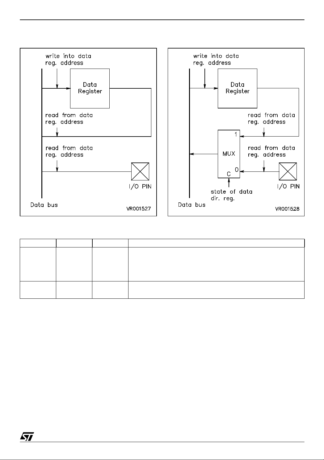
Fi
Fi
gure 2. Data register access
gure 3. Read multiplexing
Table 1. Input and output modes of an I/O cell
DDR OR DR I/O pin input/output modes
0 0 0 input with pull-up
0 0 1 input no pull-up
0 1 0 interr up t input with pull-u p
0 1 1 analog input
1 0 DR open drain output
1 1 DR push-pull output
For most microco ntrollers which use p rogrammable flex ibility for I/O pins, it has bee n
common, to reduce the number of registers, to use the data register address for 3 purposes:
– writing to the DR
– reading the DR content
– reading the state of the I/O pin.
With this convention, the data read from the DR register may come from two different sources,
the DR output and the I/O pin. The source is selected by a multiplexer controlled by the state
of the DDR.
If the DDR bit corresponding to the I/O pin contains a “1", the port pin is set to output. Subsequent read accesses to DR will return the content of the DR.
3/12
Page 4

USING ST62xx I/O PORTS SAFELY
If the DDR bit corresponding to the I/O pi n contains a “0 ", the port pin i s set to input. Subsequent read accesses to DR will return the state of the I/O pi n. T his means that the D R bit i s effectively Read Only when the bi t is in O utput mod e. To r ead the content of any DR bi t set to
input mode a copy of the DR content previously written must be saved in Data RAM.
Writing to the DR bit is possible in both input and output modes. It is important to note this as
in input mode, DR is used to set the input pin characteristics (table 1). Due to the flexibility of
programming each I/O bit i ndividually, s ome p ins of a port may b e configur ed to input mode
and others to output mod e. Reading the DR will re turn some D R bit contents (from p ins in
output mode) and some I/O pin states (from pins in input mode) combined in the one byte. As
will be shown in a following section this can create serious system malfunctions if care is not
taken.
4/12
Page 5

USING ST62xx I/O PORTS SAFELY
2 I/O PIN OPTIONS
Each ST62 I/O pin with Analog capability can work as:
– a push-pull output
– an open drain output
– a schmitt trigger input with internal 100K pull-up
– a schmitt trigger input without pull-up
– an interrupt input with schmitt trigger and internal 100K pull-up
– an analog input (connected to the Analog to Digital converter)
As described in the previous section,
– each bit of the I/O port can have different characteristics
– each bit is completely independent of the others
– each bit has its own control bits defining its operation mode
– the bit operation modes can be changed by software at any time
Figure 4. I/O port with pins in different functions
An example of a potential I/O port configuration is shown in Figure 4. Pin 0 is in push pull
output mode, outputting a high level, pin 1 is in open drain output mode and presents a high
impedance (this is because DR is 1, causing the pull-down resistor to be turned off). Pin 2 is
in input mode with pull-up, pin 3 is in input mode without pull-up, while pins 4 and 5 are interrupt inputs, pin 6 is analog input and pin 7 is an input without pull-up.
Only one pin of an ST62XX should be switched to analog input mode at any time. Otherwise,
all pins switched to analog input mode will b e connected to gether via the analog sw itches
(RDSON = 1/4 kΩ)
5/12
Page 6

USING ST62xx I/O PORTS SAFELY
When using the interrupt input with more than one pin configured for this function, all pins will
be connected together in a logical “AND” function to the same core interrupt input line. A low
signal at any of the inputs will pull the core interrupt line low, si gnifying an interrupt event. To
get a high signal at the core interrupt line ALL interrupt inputs must be high.
Figure 5. Interrupt schematic for one I/O pin
6/12
Page 7

USING ST62xx I/O PORTS SAFELY
3 OPERATION OF SINGLE BI T INSTRUCTIONS
The ST62XX instruction set includes four different instructions operating on single bits.
The first two instructions use a read-modify-write cycle.
– SET Set Bit in Register
– RES Reset Bit in Register
– JRS Jump Relative IF Bit in Regis ter is se t
– JRR Jump Relative IF Bi t in R egister is reset
The single bit instructions read a whole byte (8 bits), perform an “AND” (RES, JRR) or “OR”
(SET, JRS) operation with a single bit mask operand (e.g 01h for bit 0, 04h for bit 2), and, in
the case of SET and RES, write the result back to the source.
Thus the whole byte is pr ocessed, even i f onl y one bit is modified or test ed. This c auses some
constraints in using these instructions with the Data Register.
Table 2. Example for the operation of a single bit instruction
RAM (Before) RAM (After)
Address Data Address Data
SET 3,085h
085h 055h 055h 01010101 B 085h 05Ch
OR 008h 00001000 B
05Ch 01011101 B
Restrictions in using SET and RES instructions
As an example, let us assume that one or more of the pins of the port are set to input mode.
A SET/RES operation on a bit of DR will read the state of the corresponding input pin instead
of the content of DR. After modifying the specified bit, the result will be written (as a byte) back
into DR.
Depending on the state of the specified inputs, the contents of DR may be changed. This can
cause a c ha nge of th e input mo de by a ccident , tha t is, depe nding on t he state of the co rresponding bit in OR, the pin operation mode can be switched from input mode with pull-up to
input mode without pull-up (or vice-versa) or from interrupt mode to analog input (or viceversa). These side effects on the I/O port may be avoided if a copy of the DR content is kept
in a RAM location. Now SET/RES instructions can be executed on the RAM location, and the
result then written to DR as shown in Table 3.
7/12
Page 8

USING ST62xx I/O PORTS SAFELY
Table 3. Example of a SET sequen ce wit h RAM buffer for DR
DRA .def 00ch, 0ffh, 0ffh ; DR of IOP3
DRBUFF .def 090h, 0ffh, 0ffh ; buffer for IOP3 DR
...
SET 2, DRBUFF
LD A, DRBUFF
LD DRA, A
...
Such a sequence is only required for DR address when some bits are set to input. No restrictions apply for operating on OR or DDR.
It is recommende d that the OR should be used prim arily for switching of pin input operating
modes. This r egister s witches th e port bits from inp ut witho ut pull-up to analo g input, or
switches from input mode with pull-up to interrupt input with pull-up. Transition diagrams
showing the optimum coding sequence for modifying the states are shown in the following figures.
8/12
Page 9

USING ST62xx I/O PORTS SAFELY
4 MODE TRAN SITION DIAGRAMS
Figure 6. shows the recommended transfer seq uence for changing from one state to another
(no other transitions should be used).
Figure 6. Diagram for safe transitions
Figure 7. illustrates the transitions which are most likely to cause a change of operation mode
causing unwanted side effects such as false interrupt generation or two pins being shorted together via the analog input line.
9/12
Page 10

USING ST62xx I/O PORTS SAFELY
Figure 7. Diagram for risky transitions
Figure 8. demons trat es the False t rans ition s that can o ccur wi th SET /RE S ins tructi ons de -
pending on the state of the I/O pins.
10/12
Page 11

USING ST62xx I/O PORTS SAFELY
Figure 8. Diagram for I/O data register F alse transitions
11/12
Page 12

USING ST62xx I/O PORTS SAFELY
“THE PRESENT NOTE WHICH IS FOR GUIDANCE ONLY AIMS AT PROVIDING CUSTOMERS WITH INFORMATION
REGARDING THE IR PRO DUCT S IN OR DER FO R THEM TO SAV E TIME . AS A RES ULT, STMIC ROEL ECTR ONI CS
SHALL NOT BE HELD LIABLE FOR ANY DIRECT, INDIRECT OR CONSEQUENTIAL DAMAGES WITH RESPECT TO
ANY CL AIM S AR IS IN G FR OM T HE CO N TENT OF S UC H A NO TE A ND /O R T HE U SE M AD E BY C US TO ME RS O F
THE INFORMATION CONTAINED HEREIN IN CONNECTION WITH THEIR PRODUCTS.”
Information furnished is believed to be accurate and reliable. However, STMicroelectronics assumes no responsibility for the consequences
of use of such information nor for any infringement of patents or other rights of third parties which may result from its use. No license is granted
by implic ation or oth erwise under any patent or patent rights of STMicroel ectronics. S pecificati ons mentioned in this publication are subject
to change without notice. This publication supersedes and replaces all information previously supplied. STMicroelectronics products are not
authorized for use as critical components in life support devices or systems wi thout expres s written approval of STMicroelectronics.
The ST logo is a registered tradema rk of STMicroe l ectronics.
All other n am es are the pro perty of their respective owners
© 2003 STMi croelectro ni cs - All rights reserved
STMicroelectronics GROUP OF COMPANIES
Australi a – B elgium - Braz il - Canada - China – Czech Republic - Finl and - France - Germany - Hong Kong - India - Israel - Ital y - Japan -
Malaysia - Malta - Morocco - Singapore - Spain - Sweden - Switzerland - United Kingdom - United States
www.st.com
12/12
 Loading...