

Page 1

INTRODUCTION
AN431
Application note
Using ST6 analog inputs for multiple key decoding
The ST6 on-chip Analog to Digital Converter (ADC) is a useful peripheral integrated into the sili
con of the ST6 family members.The flexibility of the I/O port structure allows the multiplexing of
up to 13/8 Analog Inputs into the converter in a 28/20 pin device for the ST6210/15 2k ROM and
ST6220/25 4k ROM families, enabling full freedom in circuit layout. Many other members of the
ST6 family also offer the Analog to Digital converter.
One of the more novel and practical applications of this converter, is to decode a number ofkeys.
The technique is to connect the keys by resistive voltage dividers to the converter inputs.An example of key detection using 10 keys is illustrated in this note.
Using the Analog to Digital converter in this fashion does not require a static current and avoids
false key detection.
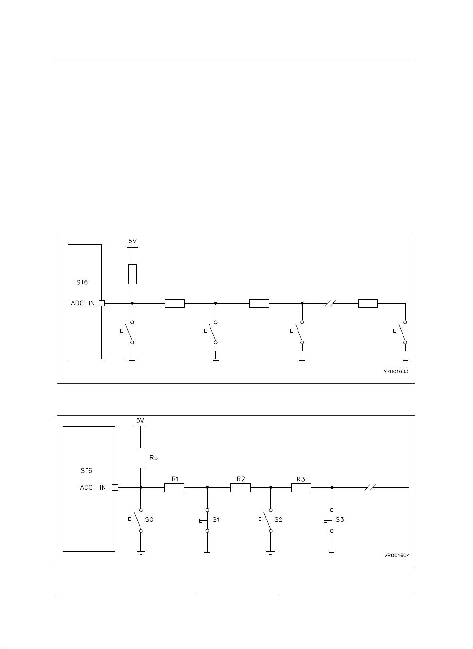
BASIC CIRCUIT
The basic circuit of the key decoder consists of a pull-up resistor connected to the ST6 Analog to
Digital converter input with the first key directly switching to ground. The following keys are then
connected in sequenceto the ADCinput through serial resistors.The number of keys which may
be detected depends on the tolerance of the resistors used. It can be seen that if more than one
key is pressed at the same time, the key detected will be the next key in the chain closest to the
ADC input. This also allows the keys in the keyboard to be prioritized.
-
June 2008
Rev 2 1/15
Page 2
ANALOG KEYBOARD
PRINCIPLE OF OPERATION
The combination of the pull-up resistor, the serial resistors and the pressed key form a resistive
voltage divider, generating a different voltage at the ADC input for each key pressed. The serial
resistors are selected in order to give an equal distribution of voltage between V
and VSSfor
DD
each switch combination to give the best noise margin between keys.
When a key is pressed, the voltage at the ADC input is given by the activated voltage divider.
This analog voltage is converted by the ADC and the digital value is used to determine which
switch is closed. Two successive conversions may be madeto avoid the influence of key bounce.
If the top key is pressed, the voltage measured is always zero.For n keys, the resistor values should
be selected such that the voltage for the second key from top is V
/n, for the 3rd - 2xVDD/n, for the
DD
Figure 1. Analog Keyboard resistor key matrix
Figure 2. Multiple key press
2/15
Page 3
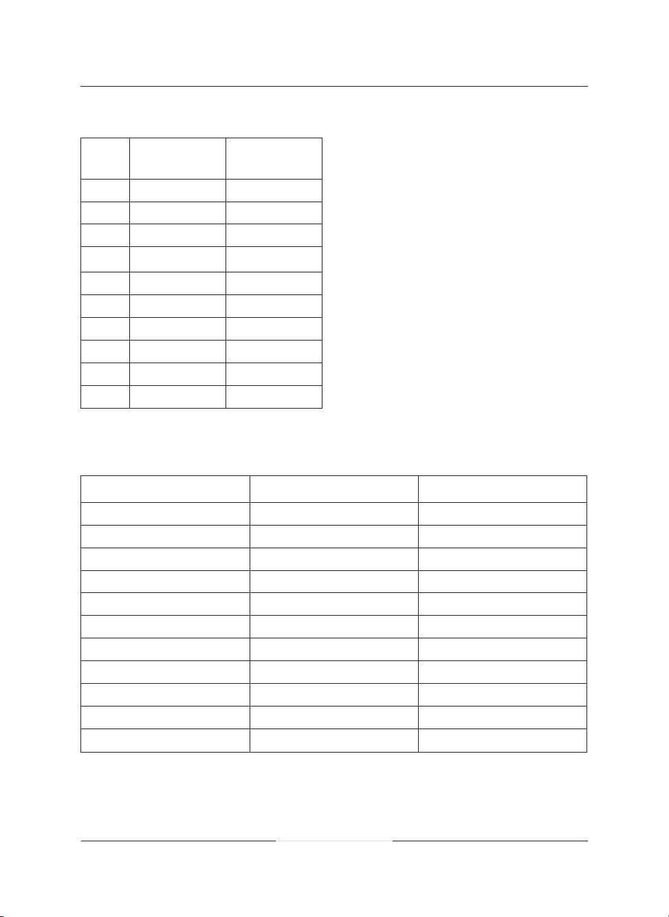
Table 1. Key code ranges
Key Nr
10 E5-E6 25
Valid Code
Range
10 24
2 18-1A 22
3 30-33 22
4
5 63-68 20
6 7C-81 22
7 97-9B 21
8 B0-B4 22
9 CA-CD 24
49-4E 21
Distance to
next key
Table 2. Used resistors and Tolerance
ANALOG KEYBOARD
4th - 3xV
/n and for the nth - (n-1)xVDD/n. Re
DD
sistor values from the tolerance set used
must be selected to meet this requirement.
The recommended resistor values for a
10-key keyboard with 2% resistors from the
E24 series, used with a 10kΩ pull-up resistor,
are shown intable 2. If more current can be al
lowed, then a 1kΩ resistor can be used in
which case the serial resistor values should
be divided by 10.
-
-
Resistor
Rp 10000 9800
R1 1100 1078
R2 1300 1274
R3 1800 1764
R4 2400 2352
R5 3300 3234
R6 5100 4998
R7 8200 8036
R8 16000 15680
Active Key R Error Range (LSB) Distance to next Key
S0 0 24
Value ( ) -2% ( )
3/15
Page 4
ANALOG KEYBOARD
PRACTICAL LIMITATIONS
Theoretically, for an ideal power supply, ADC and resistors, 255 keys could be detected. Practi
cally however, it is necessary to take into account potential errors coming from:
- the power supply - the key resistivity - the resistor tolerance - the ADC error
The power supply tolerance can normally be neglected providing noise is not present at a fre
quency within or above the frequency range of the RC delay of the resistive divider, as the ADC
reference is normally provided by the powersupply of the ST6. For ST6 family members with ex
ternal ADC reference voltage inputs, AV
and AVSSmay be used instead of VDDand VSS.
DD
The sensitivity of the key can normally be neglected, as the resistance of the divider is high in
comparison to it. If the key resistivity is significant, it should be added to the “serial” pull-down re
sistance of the different dividers. The key resistivity variation must also be added to the toler
ance of the serial pull-down resistor (see resistor tolerance following).
The resistor tolerance affects the tolerance of the dividers. Two situations must be taken into ac
count:
a) minimum value of pull-up combined withmaximum values of pull-down = maximum voltage of
the divider at the ADC input.
b) maximum value of the pull-up combined with the minimum values of pull-down = minimum
voltage at the ADC input. These two cases give the maximum voltage variation of each divider
(see Table 3). The voltage variation ranges of two dividers must not overlap otherwise the key
cannot be decoded, even with an ideal converter.
Table 3. Effective Divider Resistors RX
Active
Key
S0
S1
S2
S3
S4
S5
S6
S7
S8
S9
R -2% ( ) R +2% ( )
00
1078 1122
2352 2448
4116 4284
6468 6732
9702 10098
14700 15300
22736 23664
38416 39984
88396 92004
Realistic converters require a margin between the range of variation. In the case of a
significant variation in the key resistivity, the
maximum resistivity of the key has to be
added to the value of the pull-down resistor in
case a). For case b) no error needs to be
added as the resistivity cannot be less than 0
Ω.
-
-
-
-
-
-
4/15
Page 5
ANALOG KEYBOARD
The linearity of the ADC converter of the ST6 is normally specified for ⎛2 LSB, therefore a minimum
distance of 4 LSB is needed between the edges of the resistance tolerance ranges.For the best re
sults, a minimum of 8 LSB should be used (see Table 4).
Table 4. Voltage at the ADC-Input,Converter Results (5V supply)
V (Rxmin-Rpmax) V (Rxmax-Rpmin)
Active Key
V hex. dec. V hex. dec.
S0 0.00 00 0 0.00 00 0
S1 0.48 18 24 0.51 1A 26
S2 0.94 30 48 1.00 33 51
S3 1.44 49 73 1.52 4E 78
S4 1.94 63 99 2.04 68 104
S5 2.44 7C 124 2.54 81 129
S6 2.95 97 151 3.05 9B 155
S7 3.45 B0 176 3.54 B4 180
-
S8 3.95 C9 201 4.02
Table 5. AD-Converter Results
Active Key
S0 0 24 0-0
S1 2 22 18-1A
S2 3 22 30-33
S3 4 21 49-4E
S4 5 20 63-68
S5 5 22 7C-81
S6 5 21 97-9B
S7 4 22 B0-B4
S8 3 24 C9-CD
S9 2 25 E5-E6
R Error Range
(LSB)
Distance to next
Key
CD
Valid Key Range
205
5/15
Page 6

ANALOG KEYBOARD
EXTENSION FOR WAKE UP
ST6 family members with the Analog input
capacity can also generate a wake-up opera
tion (from WAIT or STOP modes) on the
pressing of a key. This can be achieved by a
modification of the circuit shown in figure 1.
The pull-up resistor is not connected to V
DD
but to an additional I/O port bit. During key
polling, this additional port bit is set to output
mode active high, thus effectively switching
to the pull-up resistor. The resistance of
V
DD
the pull-up resistor must be high enough to
give no significant voltage drop, or the result
ing error must be calculated and taken into
account. The other I/O bit is used as the Ana
log input tothe ADC as in theoriginal circuit.
During the wait for the key press, the first I/O
pin, used to pull the pull-up resistor high to
while polling, is switched into a high im-
V
DD
pedance state (e.g. open drain output mode).
The second I/O pin, used as the ADC input
while polling, is switched to the interrupt input
with pull-up mode. The internal pull-up is in
the range of 100k, in comparison to the 1k 10k of the external resistor used during polling. If any key is now pressed an interrupt will
be generated if the voltage at the second I/O
pin is below the Schmitt trigger low level
threshold.The serial resistors in the keyboard
chain must not be too high in this case, therefore the maximum number of keys is reduced
in comparison to the normal mode.
Figure 3. Keyboard wake-up circuit
-
-
-
Figure 4. Keyboard reading
6/15
Figure 5. Interrupt configuration
Page 7

ANALOG KEYBOARD
APPENDIX A: Key Input by Polling
;**************************************************************************
;* *
;* SGS-THOMSON GRAFING *
;* *
;* APPLICATION NOTE 431 - ST6 *
*
;* *
;* Use of ADC inputs for multiple key decoding *
;* *
*
;* With the inbuilt A/D converter of any ST6 it is easy to *
;* implement a small routine which enables ONE port pin, con- *
;* figured as an ADC input, to decode up to ten different switches*
;* All that is necessary is to set one port pin as an ADC input *
;* Then the program runs in an endless loop until one of the *
*
;* connected keys is pushed. *
*
;* The value from the ADC data register is then used to decide *
;* how the program will continue,on reaction to the key-push. *
*
;* *
;**************************************************************************
*
**
;***REGISTERS***
ddrpb .def 0c5h ;port B data direction register
orpb .def 0cdh ;port B option register
drpb .def 0c1h ;port B data register
adr .def 0d0h ;A/D data register
adcr .def 0d1h ;A/D control register
a .def 0ffh ;accumulator
;***CONSTANTS***
inpall .equ 000h ;used for setting all pins input
peg1_2 .equ 00ch ;border to distinguish between switch1 and switch2
peg2_3 .equ 025h ;border to distinguish between switch2 and switch3
peg3_4 .equ 03eh ;border to distinguish between switch3 and switch4
peg4_5 .equ 058h ;border to distinguish between switch4 and switch5
peg5_6 .equ 072h ;border to distinguish between switch5 and switch6
peg6_7 .equ 08ch ;border to distinguish between switch6 and switch7
peg7_8 .equ 0a5h ;border to distinguish between switch7 and switch8
peg8_9 .equ 0beh ;border to distinguish between switch8 and switch9
7/15
Page 8

ANALOG KEYBOARD
peg9_10 .equ 0d9h ;border to distinguish between switch9 and switch10
ldi ddrpb,inpall ;sets all port B pins low — all input
ldi orpb,01h ;option register:
;sets bit b0 high, the rest low
ldi drpb,01h ;direction register:
;sets bit b0 high, the rest low
;— pb0 becomes analog input
; pb1-7 become input with pull-up, but
; are not used here (only one pin may be
; analog input for A/D at the same time)
ldi adcr,30h ;A/D control register:
; 0011 0000 — -activate A/D converter
; -start conversion
; -disable A/D interrupt
loop: jrr 6,adcr,loop ;loop until the End Of Conversion bit is
;set (indicator that a conversion has
;been completed)
ld a,adr ;load acc with the result of the A/D
;conversion
;switches
; values which represent the different
sw1: cpi a,peg1_2 ;compare with peg1_2
jrnz sw2 ;A/D result was smaller than peg1_2
jp s1 ; — switch1 was pressed: jump to s1
;now the result is compared with the
sw2: cpi a,peg2_3 ;compare with peg2_3
jrnz sw3 ;A/D result was smaller than peg2_3
jp s2 ; — switch2 was pressed: jump to s2
sw3: cpi a,peg3_4 ;compare with peg3_4
jrnz sw4 ;A/D result was smaller than peg3_4
jp s3 ; — switch3 was pressed: jump to s3
sw4: cpi a,peg4_5 ;compare with peg4_5
jrnz sw5 ;A/D result was smaller than peg4_5
jp s4 ; — switch4 was pressed: jump to s4
8/15
Page 9

sw5: cpi a,peg5_6 ;compare with peg5_6
jrnz sw6 ;A/D result was smaller than peg5_6
jp s5 ; — switch5 was pressed: jump to s5
sw6: cpi a,peg6_7 ;compare with peg6_7
jrnz sw7 ;A/D result was smaller than peg6_7
jp s6 ; — switch6 was pressed: jump to s6
sw7: cpi a,peg7_8 ;compare with peg7_8
jrnz sw8 ;A/D result was smaller than peg7_8
jp s7 ; — switch7 was pressed: jump to s7
sw8: cpi a,peg8_9 ;compare with peg8_9
jrnz sw9 ;A/D result was smaller than peg8_9
jp s8 ; — switch8 was pressed: jump to s8
sw9: cpi a,peg9_10 ;compare with peg9_10
jrnz sw10 ;A/D result was smaller than peg9_10
jp s9 ; —> switch9 was pressed: jump to s9
ANALOG KEYBOARD
sw10: jp s10 ;A/D result was greater than peg9_10
; — switch10 was pressed: 0
; —> switch10 was pressed: s10
;
;*** the routines handling to the reaction to the individual key presses
;*** are to be included here.
s1:
s2:
s3:
s4:
s5:
s6:
s7:
s8:
s9:
s10:
9/15
Page 10

ANALOG KEYBOARD
APPENDIX B: Key Input by Interrupt
;**************************************************************************
;* *
;* SGS-THOMSON GRAFING *
;* *
;* APPLICATION NOTE 431 - ST6 *
;* *
;* Use of ADC inputs for multiple key decoding *
;* *
;* With the inbuilt A/D converter of any ST6 it is easy to *
;* implement a small routine with which you can recognize *
;* if one of nine connected keys is pushed by creating an *
;* interrupt. The program can then decide how it will react *
;* to the key pushed. *
;* *
;* *
;**************************************************************************
;***REGISTERS***
ddrpb .def 0c5h ;port B data direction register
orpb .def 0cdh ;port B option register
drpb .def 0c1h ;port B data register
ior .def 0c8h ;interrupt option register
adr .def 0d0h ;A/D data register
adcr .def 0d1h ;A/D control register
a .def 0ffh ;accumulator
;***CONSTANTS***
inpall .equ 000h ;used for setting all pins input
peg1_2 .equ 00ch ;border to distinguish between switch1 and switch2
peg2_3 .equ 025h ;border to distinguish between switch2 and switch3
peg3_4 .equ 03eh ;border to distinguish between switch3 and switch4
peg4_5 .equ 058h ;border to distinguish between switch4 and switch5
peg5_6 .equ 072h ;border to distinguish between switch5 and switch6
peg6_7 .equ 08ch ;border to distinguish between switch6 and switch7
peg7_8 .equ 0a5h ;border to distinguish between switch7 and switch8
peg8_9 .equ 0beh ;border to distinguish between switch8 and switch9
; en_kint (enable key-interrupt) sets the registers in a way that pushing
; any key will cause an interrupt. This subroutine must be called to
; re-enable the key interrupt (e.g. after handling the key service routine)
10/15
Page 11

ANALOG KEYBOARD
en_kint:
ldi ddrpb,inpall ;sets all port B pins low — all input
ldi orpb,02h ;option register:
; sets bit b1 high, the rest low
ldi drpb,01h ;data register:
; sets bit b0 high, the rest low
;— pb0 becomes input, no pull-up, no int
; pb1 becomes input with pull-up and int.
; pb2-7 become input with pull-up, but
; are not used here
ldi ior,10h ;interrupt option register:
;— set D4: enable all interrupts
; reset D5: falling edge on int.input(#2)
ret ;return to the calling address
;*** hd_kint (handle key interrupt) interrupt service routine
;*** evaluates the data resulting in pushing a key.
;*** Interrupt vector #2 (0ff4h and 0ff5h) must point (jump) to hd_kint.
hd_kint: ldi drpb,03h ;data register:
; 0000 0011
ldi ddrpb,01h ;data direction register:
; 0000 0001
; — pb0 becomes output
ldi orpb,03h ;option register:
; 0000 0011
; — pb0: push-pull output
; — pb1: ADC-input
; pb2-7 become input with pull-up, but
; are not used here
ldi adcr,30h ;A/D control register:
; 0011 0000 — -activate A/D converter
; -start conversion
; -disable A/D interrupt
loop: jrr 6,adcr,loop ;waits until the End Of Conversion
; bit is set (indicator that a conversion
; has been completed)
ld a,adr ;load acc with the result of the A/D
; conversion
;now the result is compared with the
; values which represent the different
; switches
11/15
Page 12

ANALOG KEYBOARD
sw1: cpi a,peg1_2 ;compare with peg1_2
jrnz sw2 ;A/D result was smaller than peg1_2
jp s1 ; — switch1 was pressed: jump to s1
sw2: cpi a,peg2_3 ;compare with peg2_3
jrnz sw3 ;A/D result was smaller than peg2_3
jp s2 ; — switch2 was pressed: jump to s2
sw3: cpi a,peg3_4 ;compare with peg3_4
jrnz sw4 ;A/D result was smaller than peg3_4
jp s3 ; — switch3 was pressed: jump to s3
sw4: cpi a,peg4_5 ;compare with peg4_5
jrnz sw5 ;A/D result was smaller than peg4_5
jp s4 ; — switch4 was pressed: jump to s4
sw5: cpi a,peg5_6 ;compare with peg5_6
jrnz sw6 ;A/D result was smaller than peg5_6
jp s5 ; — switch5 was pressed: jump to s5
sw6: cpi a,peg6_7 ;compare with peg6_7
jrnz sw7 ;A/D result was smaller than peg6_7
jp s6 ; — switch6 was pressed: jump to s6
sw7: cpi a,peg7_8 ;compare with peg7_8
jrnz sw8 ;A/D result was smaller than peg7_8
jp s7 ; — switch7 was pressed: jump to s7
sw8: cpi a,peg8_9 ;compare with peg8_9
jrnz sw9 ;A/D result was smaller than peg8_9
jp s8 ; — switch8 was pressed: jump to s8
sw9: jp s9 ;A/D result was bigger than peg8_9
; — switch9 was pressed: jump to s9
;
;*** The routines handling the reaction to the individual key presses
;*** are to be included here
12/15
Page 13

s1:
s2:
s3:
s4:
s5:
s6:
s7:
s8:
s9:
;*** Each routine must end with the following lines in order to enable
;*** another interrupt when the next key is pressed.
call en_kint ; enable another interrupt
return: reti
ANALOG KEYBOARD
13/15
Page 14

ANALOG KEYBOARD
Table 6. Revision history
Date Revision Description of changes
September 1992 1 Initial release
19-June-2008 2 Logo modified
14/15
Page 15

ANALOG KEYBOARD
Please Read Carefully:
Information in this document is provided solely in connection with ST products. STMicroelectronics NV and its
subsidiaries (“ST”) reserve the right to make changes, corrections, modifications or improvements, to this document,
Purchasers are solely responsible for the choice, selection and use of the ST products and services described
herein, and ST assumes no liability whatsoever relating to the choice, selection or use of the ST products and
No license, express or implied, by estoppel or otherwise, to any intellectual property rights is granted under this
document. If any part of this document refers to any third party products or services it shall not be deemed a license
grant by ST for the use of such third party products or services, or any intellectual property contained therein or
considered as a warranty covering the use in any manner whatsoever of such third party products or services or any
UNLESS OTHERWISE SET FORTH IN ST’S TERMS AND CONDITIONS OF SALE ST DISCLAIMS ANY
EXPRESS OR IMPLIED WARRANTY WITH RESPECT TO THE USE AND/OR SALE OF ST PRODUCTS
INCLUDING WITHOUT LIMITATION IMPLIED WARRANTIES OF MERCHANTABILITY, FITNESS FOR A
PARTICULAR PURPOSE (AND THEIR EQUIVALENTS UNDER THE LAWS OF ANY JURISDICTION), OR
INFRINGEMENT OF ANY PATENT, COPYRIGHT OR OTHER INTELLECTUAL PROPERTY RIGHT.
UNLESS EXPRESSLY APPROVED IN WRITING BY AN AUTHORIZED ST REPRESENTATIVE, ST PRODUCTS
ARE NOT RECOMMENDED, AUTHORIZED OR WARRANTED FOR USE IN MILITARY, AIR CRAFT, SPACE,
LIFE SAVING, OR LIFE SUSTAINING APPLICATIONS, NOR IN PRODUCTS OR SYSTEMS WHERE FAILURE
OR MALFUNCTION MAY RESULT IN PERSONAL INJURY, DEATH, OR SEVERE PROPERTY OR
ENVIRONMENTAL DAMAGE. ST PRODUCTS WHICH ARE NOT SPECIFIED AS “AUTOMOTIVE GRADE” MAY
and the products and services described herein at any time, without notice.
All ST products are sold pursuant to ST’s terms and conditions of sale.
services described herein.
intellectual property contained therein.
ONLY BE USED IN AUTOMOTIVE APPLICATIONS AT USER’S OWN RISK.
Resale of ST products with provisions different from the statements and/or technical features set forth in this
document shall immediately void any warranty granted by ST for the ST product or service described herein and shall
ST and the ST logo are trademarks or registered trademarks of ST in various countries.
Information in this document supersedes and replaces all information previously supplied.
The ST logo is a registered trademark of STMicroelectronics. All other names are the property of their respective
not create or extend in any manner whatsoever, any liability of ST.
owners.
© 2008 STMicroelectronics - All rights reserved
STMicroelectronics group of companies
Australia - Belgium - Brazil - Canada - China - Czech Republic - Finland - France - Germany - Hong Kong -
India - Israel - Italy - Japan - Malaysia - Malta - Morocco - Singapore - Spain - Sweden - Switzerland - United
Kingdom - United States of America
www.st.com
15/15
 Loading...