

Introduction
APWLink™ USB interface board
for Sound Terminal
AN4118
Application note
®
demonstration boards
This document describes APWLink™ which has been designed as a USB interface board to
control ST Sound Terminal
user manual UM1545, “Using the Audio Processor Workbench (APWorkbench)”.
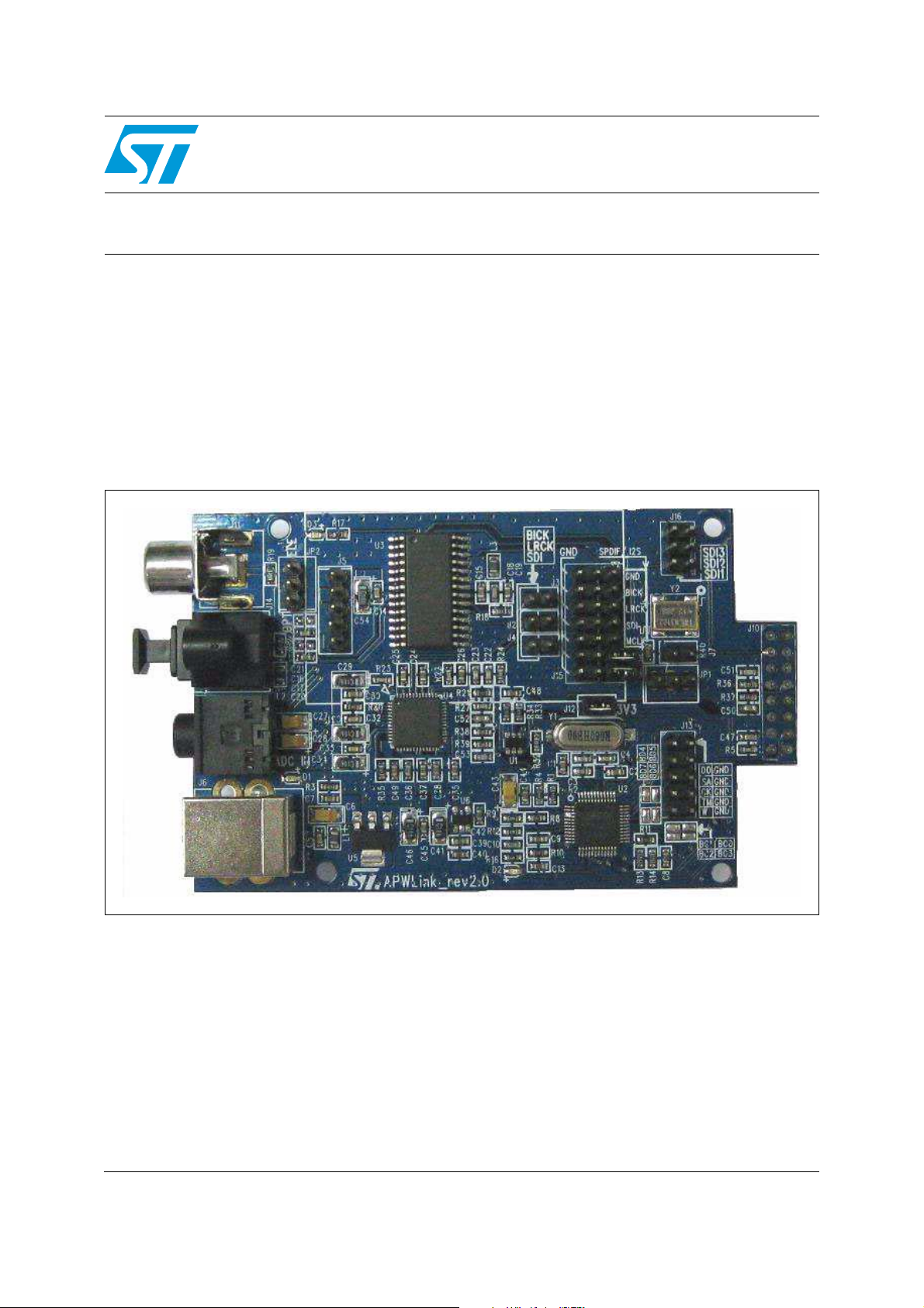
The orderable part number for APWLink™ is STEVAL-CCA035V1.
Figure 1. APWLink™ interface board (STEVAL-CCA035V1)
®
demonstration boards through APWorkbench, please refer to
June 2012 Doc ID 023226 Rev 1 1/14
www.st.com

Contents AN4118
Contents
1 Board overview . . . . . . . . . . . . . . . . . . . . . . . . . . . . . . . . . . . . . . . . . . . . . 5
2 Configuration . . . . . . . . . . . . . . . . . . . . . . . . . . . . . . . . . . . . . . . . . . . . . . . 6
2.1 Power supply . . . . . . . . . . . . . . . . . . . . . . . . . . . . . . . . . . . . . . . . . . . . . . . 6
®
2.2 3.3 V digital power output to Sound Terminal
2.3 Connection to Sound Terminal
2.4 LEDs . . . . . . . . . . . . . . . . . . . . . . . . . . . . . . . . . . . . . . . . . . . . . . . . . . . . . 7
2.5 Analog input . . . . . . . . . . . . . . . . . . . . . . . . . . . . . . . . . . . . . . . . . . . . . . . . 7
2.6 External I
2.7 Serial digital audio input . . . . . . . . . . . . . . . . . . . . . . . . . . . . . . . . . . . . . . . 8
2.8 Jumper configuration . . . . . . . . . . . . . . . . . . . . . . . . . . . . . . . . . . . . . . . . . 9
2
S input . . . . . . . . . . . . . . . . . . . . . . . . . . . . . . . . . . . . . . . . . . . . 8
®
demonstration board . . . . . . . . . . . . . . . . 6
demonstration board . . . . . 6
3 Board schematic and bill of material . . . . . . . . . . . . . . . . . . . . . . . . . . . 10
4 Revision history . . . . . . . . . . . . . . . . . . . . . . . . . . . . . . . . . . . . . . . . . . . 13
2/14 Doc ID 023226 Rev 1

AN4118 List of tables
List of tables
Table 1. Jumper configuration . . . . . . . . . . . . . . . . . . . . . . . . . . . . . . . . . . . . . . . . . . . . . . . . . . . . . . 9
Table 2. Bill of material . . . . . . . . . . . . . . . . . . . . . . . . . . . . . . . . . . . . . . . . . . . . . . . . . . . . . . . . . . . 11
Table 3. Document revision history . . . . . . . . . . . . . . . . . . . . . . . . . . . . . . . . . . . . . . . . . . . . . . . . . 13
Doc ID 023226 Rev 1 3/14

List of figures AN4118
List of figures
Figure 1. APWLink™ interface board (STEVAL-CCA035V1) . . . . . . . . . . . . . . . . . . . . . . . . . . . . . . . 1
Figure 2. System connections . . . . . . . . . . . . . . . . . . . . . . . . . . . . . . . . . . . . . . . . . . . . . . . . . . . . . . . 5
Figure 3. APWLink™ general view . . . . . . . . . . . . . . . . . . . . . . . . . . . . . . . . . . . . . . . . . . . . . . . . . . . 5
Figure 4. Connection to Sound Terminal
Figure 5. Enabling the ADC using APWorkbench . . . . . . . . . . . . . . . . . . . . . . . . . . . . . . . . . . . . . . . . 7
Figure 6. I
Figure 7. APWLink™ schematic . . . . . . . . . . . . . . . . . . . . . . . . . . . . . . . . . . . . . . . . . . . . . . . . . . . . 10
2
S input from an external ADC through J15 . . . . . . . . . . . . . . . . . . . . . . . . . . . . . . . . . . . . 8
®
demonstration board . . . . . . . . . . . . . . . . . . . . . . . . . . . . . 6
4/14 Doc ID 023226 Rev 1
AN4118 Board overview
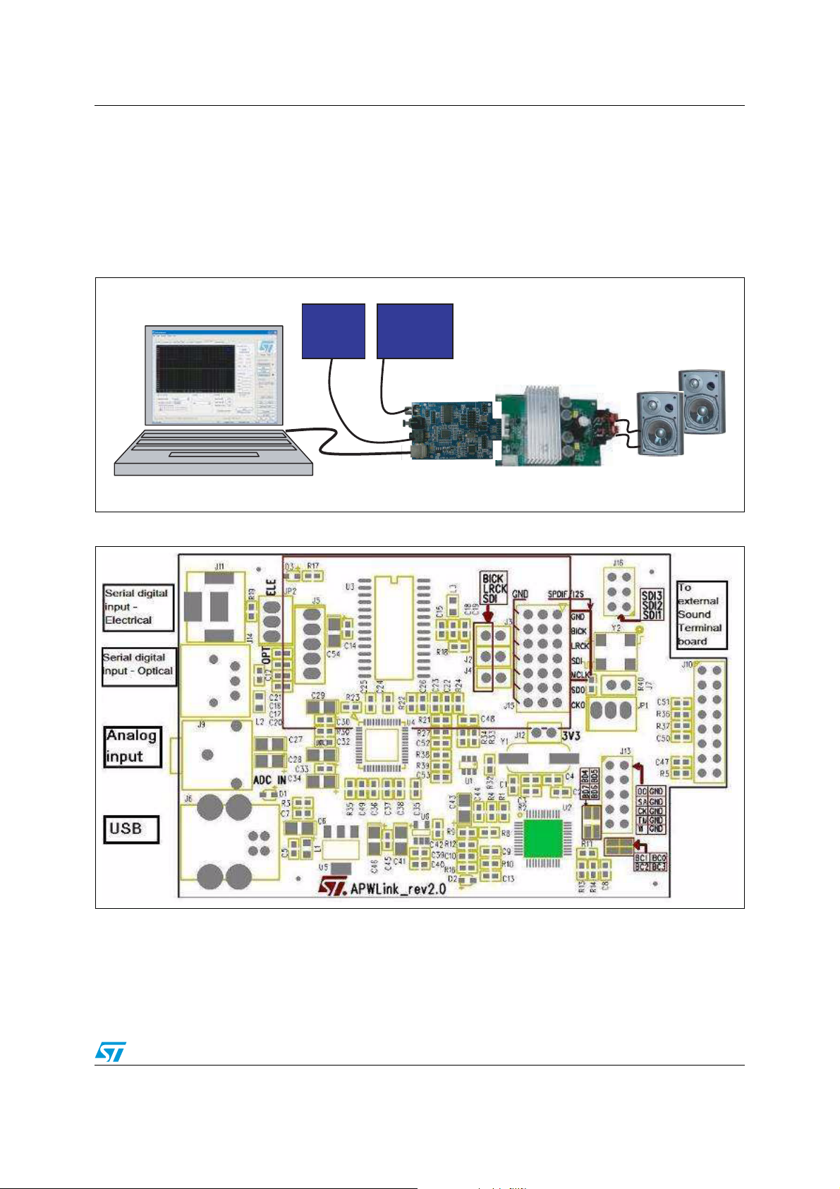
1 Board overview
In addition to providing control signals to the external Sound Terminal® demonstration
board, analog/digital audio inputs are also provided from APWLink™.
The system connections are shown below in the following figure.
Figure 2. System connections
Analog
source
APWorkbench
USB Cable
Figure 3. APWLink™ general view
Digital
source
APWLinkTM Sound Terminal® demonstration board
Doc ID 023226 Rev 1 5/14

Configuration AN4118
2 Configuration
2.1 Power supply
APWLink™ is directly powered by a USB cable (Type B). No external power supply is
needed.
Note that this power supply is NOT for the power bridge supply on the Sound Terminal
demonstration board. Please refer to the application note of each specific Sound Terminal
demonstration board.
2.2 3.3 V digital power output to Sound Terminal® demonstration board
Jumper J12 is used for the selection of the external Sound Terminal® demonstration board
digital power supply. When J12 is closed, 3.3 VDC is provided to the external Sound
Te r mi n al
has its own 3.3 V digital power supply, J12 has to be left open to avoid any current loop.
®
demonstration board, and if the external Sound Terminal® demonstration board
®
®
2.3 Connection to Sound Terminal® demonstration board
APWLink™ is simply connected to the Sound Terminal® demonstration board through J10,
an on-board 16-pin female 8x2 2.54 mm connector as shown below.
Figure 4. Connection to Sound Terminal
®
demonstration board
6/14 Doc ID 023226 Rev 1

AN4118 Configuration
2.4 LEDs
APWLink™ provides the following three LEDs:
● D1: power supply
– ON when USB power is supplied
● D2: communication wrong
– ON when communication between PC and APWLink™ is wrong
● Digital audio input error
– ON when the digital input signal is not validated or no digital signal is input
2.5 Analog input
An analog signal (can be DC coupled) can be input from J9 (3.5 mm phone jack). There is
an on-board ADC (ST part number: STA529Q) to convert the analog signal to a digital I
format signal and feed it to the external Sound Terminal
®
demonstration board. To enable
2
S
the on-board STA529Q ADC, the following actions should be taken within APWorkbench™
as shown in the screenshots below.
Figure 5. Enabling the ADC using APWorkbench
Doc ID 023226 Rev 1 7/14

Configuration AN4118
2.6 External I2S input
The external I2S signal can be input to APWLink™ through J15 directly. For example, the
external I
2
S signal can come from an external ADC if the on-board ADC is bypassed. J5
includes the analog signals from J9 (stereo analog input jack), plus 3.3 VDC power supply,
which can be fed to the external ADC. The I
APWLink™ through J15, as indicated below.
Figure 6. I
2
S input from an external ADC through J15
2.7 Serial digital audio input
2
S from the external ADC can be fed into
Electrical and optical inputs are supported on-board to receive serial digital audio signals. A
jumper (JP2) is used to select either the electrical or optical signal. The input signal is then
converted to an I
2
S format by the on-board decoder (ST part number: STA120D) and fed to
the external Sound Terminal™ demonstration board.
Serial digital formats supported by the STA120D:
● S/PDIF
● AES/EBU
● IEC 958
● EIAJ CP-340/1201
The proper jumper setting is described in Section 2.8: Jumper configuration.
8/14 Doc ID 023226 Rev 1

AN4118 Configuration
2.8 Jumper configuration
Table 1. Jumper configuration
Jumper Mode Serial digital input External I2S
On-board
J2 LR clock from STA529Q - on-board ADC Open Open Close
J3 Bit clock from STA529Q - on-board ADC Open Open Close
J4 I2S data from STA529Q - on-board ADC Open Open Close
J5 Analog output / 3.3 VDC for external ADC All open See footnote
(2)
J7 MCLK to STA529Q – on-board ADC Open Open Close
3.3 VDC to external Sound Terminal®
J12
demonstration board
Close Close Close
J13 Reserved, not used All open All open All open
Close only the relevant pins
I2S selector for external
J15
Sound Terminal® demonstration board
See footnote
(3)
(1)
ADC
All open
All open
2
I
J16
S data selector for external Sound
®
Terminal
demonstration board
All close All close All close
JP1 Reserved, not used All open All open All open
For electrical: For optical:
JP2 Serial digital audio source selector
1. APWorkbench supports on-board ADC function.
2
2. Please refer to Section 2.6: External I
3. Please refer to Section 2.6: External I
left open.
S input on page 8 for detailed signal definition for each pin.
2
S input on page 8 for detailed signal definition for relevant pins. All other pins can be
Do not care Do not care
Doc ID 023226 Rev 1 9/14

Board schematic and bill of material AN4118
3 Board schematic and bill of material
Figure 7. APWLink™ schematic
CONF_SDATAI2
CONF_LRCKI
FTDI_SDA
FTDI_RESET
FTDI_STBY
CONF_FAIL
CONF_CLKOUT
CONF_SDATAO
XTI_SPDIF
DATA_SPDIF
LRCK_SPDIF
BICK_SPDIF
FTDI_SCL
FTDI_SCL_030
789
101112
131415
161718
123
4
6
J15
5
CONF_BICKI
CONF_LRCKI
192021
CONF_CLKOUT
CONF_SDATAO
SPDT/SM
JP1
FTDI_SCL_EXT
10k
R34
10k
R33
VCC_3V3
5
6
6
'
U1
9&&
,1
1234
C48
J10
C47
47pF
R5
6*1'
STG719
100nF
VCC_3V3
BICKI_030
J4J2J3
12
LRCKI_030
SDATAI_030
J16
34
56
CONF_SDATAI1
CONF_SDATAI2
CONF_SDATAI3
0R
R7
FTDI_XTI
VCC_3V3
R40
J7
VCC_XT
4
3
2
1
R6
Y2
10k
12.288MHz
CONF_MCLKI
VCC_XT
100R
R32
J13
56
78
10R
I2C_CTRL
C11
100nF
910
CONF_TH_W
FTDI_TMODE
910
11 12
13 14
15 16
0R
J12
VCC_3V3
FTDI_MUTE
CONF_MCLKI
AUX_CON
12
34
FTDI_SA
CONF_CLKOUT
CONF_SDATAO
100R
R37
12
34
56
78
100R
R36
CONF_BICKI
FTDI_SCL_EXT
CONF_SDATAI1
CONF_SDATAI3
J5
12345
VCC_3V3
C41
10uF
C50
120pF
MB_CON
C55
100uF
+
C51
10pF
AINL
AINR
AGND
+
C42
100nF
5
Vout
BYPASS
Vin
GND
INH
U6
LD2985A18
1234
C40
100nF
1uF
C39
VCC_USB VCC_1V8
+
C46
VCC_3V3
10uF
C45
100nF
GND
Vout
Vin
AP1117_33
Vout
U5
C44
100nF
33uF
C43
+
VCC_USB
I2C_CTRL
FTDI_SCL
FTDI_RESET
FTDI_STBY
FTDI_MUTE
TP9
TP3
TP4
TP5
TP1
TP2
TP8
TP6
TP7
TP12
TP10
TP11
FTDI_SDA
TP13
TP14
DATA_SPDIF
VCC_3V3
VCC_3V3
R13
5k1
5k1
R14
C8
100nF
10k
36
%'%86
%'%86
%'%86
37
%'%86
38
%'%86
39
C2
100nF
VCC_USB
C4
27pF
C3
Y1
27pF
R3
470R
VCC_USB VCC_USB
L1
BEAD
%'%86
40
3:5(1
41
9&&
42
;7,1
43
U2
;7287
1M
44
$*1'
45
R2
$9&&
46
7(67
47
((&6
48
6.000MHz
R1
D1
C7
C6
+
C5
10nF
((6.
C1
470R
(('$7$
100nF
123456789
10k
R4
Green
100nF
33uF
R11
*1'
9&&,2%
%&%86
%'%86
%'%86
6,:8%
%&%86
%&%86
%&%86
FT2232D
9&&
5(6(7
567287
9287
86%'3
86%'0
*1'
6,:8$
$&%86
101112
R8
1k5
10k
R10
27R
27R
R9
R12
VCC_3V3
C10
123
4
'
'
*1'
9%86
J6
0R
2526272829303132333435
R15
*1'
$'%86
24
$'%86
23
$'%86
22
$'%86
21
$'%86
20
$'%86
19
*1'
18
$'%86
17
$'%86
16
$&%86
15
9&&,2$
14
$&%86
13
$&%86
C9
33nF
VCC_3V3
C13
100nF
470R
R16
D2
Red
47pF
VCC_USB VCC_3V3
USB
FTDI_SA
FTDI_XTI
CONF_FAIL
CONF_TH_W
FTDI_TMODE
9(5)
& 28
1
L2
D3
R17
27
2625242322
(5)
&H)
6'$7$
&E(
&G)
&F)
4
3
2
+
C54
BEAD
J9
Blue
C14
C12
123
XTI_SPDIF
BEAD
4R7
L3
R20
C15
100nF
470nF
C19
330R
560R
R18
20
21
0
0
9$
),/7
0&.
$*1'
U3
STA120 D
'*1'
5;3
9'
&(
&D(
5;1
5
9
6
7
8
10
100nF
10uF
C17
100nF
C16
JP2
100nF
96
*1'
'$7$
*3)$95.
J11
15nF
C18
SPDT/SM
0
)6<1&
11
C21
100nF NS
R19
171819
0
6&.
12
100nF NS
C20
100nF
82R
LRCK_SPDIF
BICK_SPDIF
CONF_MCLKI
FTDI_SDA
FTDI_SCL_030
VCC_3V3
100R
100R
C53
10pF
R38
R39
C35
0R
R24
C22
220pF
0R
C23
82pF
R27
12k
R21
XTI
XTO
MCLK33
FILT
C26
100nF
40
GNDPLL
41
0R
R22
VCC_1V8
15
16
&%/
6(/
8
&6)&.
14
13
VDDPLL
42
GND2
43
VDD2
44
SDATAI
45
C24
SDATAO
100nF
46
LRCLKI
47
LRCLKO
48
GNDIO2
49
VDDIO2
50
BICLKI
51
BICLKO
52
STBY
INL
INR
123456789
C25
100nF
VCC_3V3
0R
R23
+
VCC_3V3
BICKI_030
LRCKI_030
SDATAI_030
+
1uF
C27
4k7
R25
2
1
3
AINL
AINR
J14
100nF
C52
120pF
TM
SCL
SDA
VCC33
I2CDIS
VDDIO1
SELCLK33
PWRFAULT/EADP
U4
STA030 / STA529 Q
VBIAS
AVDD
VHI
VLO
AGND
VCM
RST_N
CLKOUT
101112
10uF
+
10nF
C32
10nF
C34
C33
10uF
+
C31
470R
C30
100nF
R30
+
1uF
10uF
C29
C28
10k
4k7
R28
R35
R29
4k7
4k7
R26
AGND
0R
R31
VCC_3V3
27282930313233343536373839
GND33
GNDIO1
VCC2A
26
OUT2A
25
GND2A
24
GND2B
23
OUT2B
22
VCC2B
21
VCC1B
20
1uF
C38
OUT1B
19
GND1B
18
GND1A
17
OUT1A
16
C37
100nF
VCC1A
15
MUTE
14
VDD1
GND1
13
C36
100nF
Y#PV
C49
100nF
VCC_1V8
VCC_3V3
ADC_IN
10/14 Doc ID 023226 Rev 1

AN4118 Board schematic and bill of material
Table 2. Bill of material
Item Qty Reference Part name Value Footprint Remarks
1 1 U1 IC STG719 SOT23-6L
2 1 U2 IC FT2232D LQFP48
3 1 U3 IC STA120D SO28
4 1 U4 IC STA529Q VFQFPN52
5 1 U5 IC LD1117 SOT223
6 1 U6 IC LD2985B18 SOT23-5L
7 1 D1 LED Green 0603
8 1 D2 LED Red 0603
9 1 D3 LED Blue 0603
10 3 L1-3 Ferrite bead 600 ohms / 100 MHz 0805
11 1 Y1
12 1 Y2
13 5 J2-4, J7, J12 Header Header 2 x 1 2.54 mm x 2
14 1 J5 Header Header 5 x 1 2.54 mm x 5
15 1 J6
16 1 J9
17 1 J10
18 1 J11 RCA RCA connector RCA
19 1 J13 Header Header 5 x 2 2.54 mm x 5 x 2
20 1 J14
21 1 J15 Header Header 7 x 3 2.54 mm x 7 x 3
22 1 J16 Header Header 3 x 2 2.54 mm x 3 x 2
23 2 JP1-2 Header Header 3 x 1 2.54 mm x 3
C1-2, C7-8, C11-16, C20,
24 24
25 2 C17, C21 CAP 100 nF NS 0603 Not fitted
C24-26, C30, C35-37, C40,
C42, C44-45, C48-49
Crystal,
6.000 MHz
Oscillator,
12.288 MHz
USB
connector
Optical
receiver
Female
connector
Headphone
jack
CAP 100 nF 0603
6.000 MHz XTAL_HC49SMT
12.288 MHz SMD, 7 mm x 5 mm
Type B Type B
GP1F31R
Female 8 x 2 2.54 mm x 8 x 2
Stereo headphone jack
bottom
side
26 3 C5, C32-33 CAP 10 nF 0603
27 2 C51, C53 CAP 10 pF 0603
28 2 C50, C52 CAP 120 pF 0603
29 1 C18 CAP 15 nF 0603
Doc ID 023226 Rev 1 11/14

Board schematic and bill of material AN4118
Table 2. Bill of material
Item Qty Reference Part name Value Footprint Remarks
30 2 C38-39 CAP 1 µF 0603
31 1 C22 CAP 220 pF 0603
32 2 C3-4 CAP 27 pF 0603
33 1 C9 CAP 33 nF 0603
34 1 C19 CAP 470 nF 0603
35 2 C10, C47 CAP 47 pF 0603
36 1 C23 CAP 82 pF 0603
37 1 C55
38 6 C29, C31, C34, C41, C46, C54
39 2 C27-28
40 2 C6, C43
41 8
42 5 R32, R36-39 RES 100R 0603
43 1 R40 RES 10R 0603
44 7 R4, R6, R10-11, R33-35 RES 10K 0603
45 1 R21 RES 12K 0603
46 1 R2 RES 1M 0603
47 1 R8 RES 1K5 0603
48 2 R9, R12 RES 27R 0603
49 1 R18 RES 330R 0603
50 4 R1, R3, R16, R30 RES 470R 0603
51 1 R20 RES 4R7 0603
R5, R7, R15, R22-24, R27,
R31
Tantalum-
CAP
Tantalum-
CAP
Tantalum-
CAP
Tantalum-
CAP
RES 0R 0603
100 µF Sized
10 µF 1206
1 µF 1206
33 µF 1206
52 4 R25-26, R28-29 RES 4K7 0603
53 1 R17 RES 560R 0603
54 2 R13-14 RES 5K1 0603
55 1 R19 RES 82R 0603
12/14 Doc ID 023226 Rev 1

AN4118 Revision history
4 Revision history
Table 3. Document revision history
Date Revision Changes
22-Jun-2012 1 Initial release.
Doc ID 023226 Rev 1 13/14

AN4118
Please Read Carefully:
Information in this document is provided solely in connection with ST products. STMicroelectronics NV and its subsidiaries (“ST”) reserve the
right to make changes, corrections, modifications or improvements, to this document, and the products and services described herein at any
time, without notice.
All ST products are sold pursuant to ST’s terms and conditions of sale.
Purchasers are solely responsible for the choice, selection and use of the ST products and services described herein, and ST assumes no
liability whatsoever relating to the choice, selection or use of the ST products and services described herein.
No license, express or implied, by estoppel or otherwise, to any intellectual property rights is granted under this document. If any part of this
document refers to any third party products or services it shall not be deemed a license grant by ST for the use of such third party products
or services, or any intellectual property contained therein or considered as a warranty covering the use in any manner whatsoever of such
third party products or services or any intellectual property contained therein.
UNLESS OTHERWISE SET FORTH IN ST’S TERMS AND CONDITIONS OF SALE ST DISCLAIMS ANY EXPRESS OR IMPLIED
WARRANTY WITH RESPECT TO THE USE AND/OR SALE OF ST PRODUCTS INCLUDING WITHOUT LIMITATION IMPLIED
WARRANTIES OF MERCHANTABILITY, FITNESS FOR A PARTICULAR PURPOSE (AND THEIR EQUIVALENTS UNDER THE LAWS
OF ANY JURISDICTION), OR INFRINGEMENT OF ANY PATENT, COPYRIGHT OR OTHER INTELLECTUAL PROPERTY RIGHT.
UNLESS EXPRESSLY APPROVED IN WRITING BY TWO AUTHORIZED ST REPRESENTATIVES, ST PRODUCTS ARE NOT
RECOMMENDED, AUTHORIZED OR WARRANTED FOR USE IN MILITARY, AIR CRAFT, SPACE, LIFE SAVING, OR LIFE SUSTAINING
APPLICATIONS, NOR IN PRODUCTS OR SYSTEMS WHERE FAILURE OR MALFUNCTION MAY RESULT IN PERSONAL INJURY,
DEATH, OR SEVERE PROPERTY OR ENVIRONMENTAL DAMAGE. ST PRODUCTS WHICH ARE NOT SPECIFIED AS "AUTOMOTIVE
GRADE" MAY ONLY BE USED IN AUTOMOTIVE APPLICATIONS AT USER’S OWN RISK.
Resale of ST products with provisions different from the statements and/or technical features set forth in this document shall immediately void
any warranty granted by ST for the ST product or service described herein and shall not create or extend in any manner whatsoever, any
liability of ST.
ST and the ST logo are trademarks or registered trademarks of ST in various countries.
Information in this document supersedes and replaces all information previously supplied.
The ST logo is a registered trademark of STMicroelectronics. All other names are the property of their respective owners.
© 2012 STMicroelectronics - All rights reserved
STMicroelectronics group of companies
Australia - Belgium - Brazil - Canada - China - Czech Republic - Finland - France - Germany - Hong Kong - India - Israel - Italy - Japan -
Malaysia - Malta - Morocco - Philippines - Singapore - Spain - Sweden - Switzerland - United Kingdom - United States of America
www.st.com
14/14 Doc ID 023226 Rev 1
 Loading...