

Page 1

AN4092
Application note
Hw recommendations for SPC564Axx / SPC563Mxx
Introduction
The SPC564Axx /SPC563Mxx devices target a range of powertrain applications:
● Low to mid range engine management
● Automotive transmission control
The devices are based on the e200zx Power Architecture
version of the enhanced Timing Processor Unit (eTPU2) for advanced, independent timing
control operations.
This document aims to provide guidelines to design the ECU hardware in the most efficient
way. It is focused on:
● Power Management Controller (PMC)
● FMPLL and oscillator
● Configuration pins and unused IOs
● ADC see Section 4: ADC
● Reset
®
core and feature the second
May 2012 Doc ID 023080 Rev 1 1/38
www.st.com
Page 2

Contents AN4092
Contents
1 Power Management Controller (PMC) . . . . . . . . . . . . . . . . . . . . . . . . . . . 6
1.1 Single 5 V system power supply . . . . . . . . . . . . . . . . . . . . . . . . . . . . . . . . 6
1.1.1 External power supply slew rate . . . . . . . . . . . . . . . . . . . . . . . . . . . . . . . 6
1.1.2 3.3 V power supply . . . . . . . . . . . . . . . . . . . . . . . . . . . . . . . . . . . . . . . . . 6
1.1.3 1.2 V power supply and regulator controller . . . . . . . . . . . . . . . . . . . . . . 7
1.1.4 External ballast transistor . . . . . . . . . . . . . . . . . . . . . . . . . . . . . . . . . . . . 7
1.1.5 1.2V core regulator external circuitry . . . . . . . . . . . . . . . . . . . . . . . . . . . . 8
1.1.6 Inrush current . . . . . . . . . . . . . . . . . . . . . . . . . . . . . . . . . . . . . . . . . . . . . 11
1.1.7 Layout recommendations . . . . . . . . . . . . . . . . . . . . . . . . . . . . . . . . . . . . 12
1.2 External power supply configuration . . . . . . . . . . . . . . . . . . . . . . . . . . . . 14
1.2.1 Decoupling . . . . . . . . . . . . . . . . . . . . . . . . . . . . . . . . . . . . . . . . . . . . . . . 15
1.2.2 External power supply slew rate . . . . . . . . . . . . . . . . . . . . . . . . . . . . . . 15
1.2.3 Power up/down sequencing . . . . . . . . . . . . . . . . . . . . . . . . . . . . . . . . . . 15
1.3 Mixed configurations . . . . . . . . . . . . . . . . . . . . . . . . . . . . . . . . . . . . . . . . 15
1.4 Low-Voltage-Inhibit (LVI) . . . . . . . . . . . . . . . . . . . . . . . . . . . . . . . . . . . . . 15
1.5 Voltage fine tuning . . . . . . . . . . . . . . . . . . . . . . . . . . . . . . . . . . . . . . . . . . 16
1.6 Stand-by RAM functionality . . . . . . . . . . . . . . . . . . . . . . . . . . . . . . . . . . . 16
1.6.1 SRAM Standby switch . . . . . . . . . . . . . . . . . . . . . . . . . . . . . . . . . . . . . . 16
1.6.2 Standby Regulator . . . . . . . . . . . . . . . . . . . . . . . . . . . . . . . . . . . . . . . . . 17
1.6.3 Brown-out Detector . . . . . . . . . . . . . . . . . . . . . . . . . . . . . . . . . . . . . . . . 17
1.7 Power dissipation . . . . . . . . . . . . . . . . . . . . . . . . . . . . . . . . . . . . . . . . . . . 17
1.7.1 Internal logic power consumption . . . . . . . . . . . . . . . . . . . . . . . . . . . . . 18
1.7.2 Analog power consumption . . . . . . . . . . . . . . . . . . . . . . . . . . . . . . . . . . 18
1.7.3 Voltage regulator power consumption . . . . . . . . . . . . . . . . . . . . . . . . . . 18
1.7.4 3.3V power consumption . . . . . . . . . . . . . . . . . . . . . . . . . . . . . . . . . . . . 18
1.7.5 IOs power consumption . . . . . . . . . . . . . . . . . . . . . . . . . . . . . . . . . . . . . 18
1.7.6 Package power dissipation . . . . . . . . . . . . . . . . . . . . . . . . . . . . . . . . . . 18
2 FMPLL and crystal oscillator . . . . . . . . . . . . . . . . . . . . . . . . . . . . . . . . . 19
2.1 Crystal oscillator and external circuitry . . . . . . . . . . . . . . . . . . . . . . . . . . . 19
2.1.1 External circuitry . . . . . . . . . . . . . . . . . . . . . . . . . . . . . . . . . . . . . . . . . . 20
2.1.2 Recommended crystals . . . . . . . . . . . . . . . . . . . . . . . . . . . . . . . . . . . . . 21
2.2 Crystal or external reference . . . . . . . . . . . . . . . . . . . . . . . . . . . . . . . . . . 21
2/38 Doc ID 023080 Rev 1
Page 3

AN4092 Contents
2.3 Bypass mode or normal mode . . . . . . . . . . . . . . . . . . . . . . . . . . . . . . . . . 21
2.4 Ramp up . . . . . . . . . . . . . . . . . . . . . . . . . . . . . . . . . . . . . . . . . . . . . . . . . . 21
2.5 Layout recommendations . . . . . . . . . . . . . . . . . . . . . . . . . . . . . . . . . . . . . 22
3 Configuration pins and unused IOs . . . . . . . . . . . . . . . . . . . . . . . . . . . 23
3.1 Boot modes (SPC564Axx) . . . . . . . . . . . . . . . . . . . . . . . . . . . . . . . . . . . . 23
3.2 Boot modes (SPC563Mxx) . . . . . . . . . . . . . . . . . . . . . . . . . . . . . . . . . . . . 23
3.3 Clock reference . . . . . . . . . . . . . . . . . . . . . . . . . . . . . . . . . . . . . . . . . . . . 23
3.4 Weak pull configuration . . . . . . . . . . . . . . . . . . . . . . . . . . . . . . . . . . . . . . 24
3.5 RSTCFG (SPC564Axx only) . . . . . . . . . . . . . . . . . . . . . . . . . . . . . . . . . . 24
3.6 Unused I/Os . . . . . . . . . . . . . . . . . . . . . . . . . . . . . . . . . . . . . . . . . . . . . . . 24
4 ADC . . . . . . . . . . . . . . . . . . . . . . . . . . . . . . . . . . . . . . . . . . . . . . . . . . . . . . 25
4.1 Alternative approach . . . . . . . . . . . . . . . . . . . . . . . . . . . . . . . . . . . . . . . . 30
5 Reset . . . . . . . . . . . . . . . . . . . . . . . . . . . . . . . . . . . . . . . . . . . . . . . . . . . . . 31
5.1 /RESET . . . . . . . . . . . . . . . . . . . . . . . . . . . . . . . . . . . . . . . . . . . . . . . . . . 31
5.2 /RSTOUT . . . . . . . . . . . . . . . . . . . . . . . . . . . . . . . . . . . . . . . . . . . . . . . . . 31
5.3 Reset source description . . . . . . . . . . . . . . . . . . . . . . . . . . . . . . . . . . . . . 31
5.4 Reset circuitry example . . . . . . . . . . . . . . . . . . . . . . . . . . . . . . . . . . . . . . 33
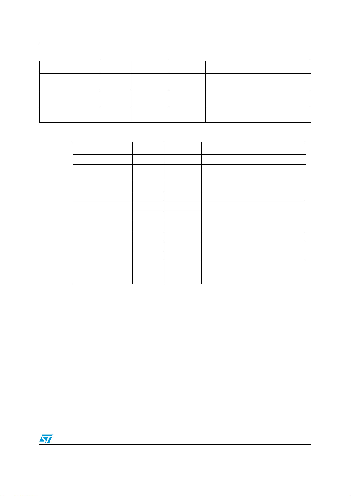
Appendix A Previous recommended PMC network configurations . . . . . . . . . 34
Appendix B Further information . . . . . . . . . . . . . . . . . . . . . . . . . . . . . . . . . . . . . . 36
B.1 Reference documents . . . . . . . . . . . . . . . . . . . . . . . . . . . . . . . . . . . . . . . . 36
Revision history . . . . . . . . . . . . . . . . . . . . . . . . . . . . . . . . . . . . . . . . . . . . . . . . . . . . 37
Doc ID 023080 Rev 1 3/38
Page 4

List of tables AN4092
List of tables
Table 1. External network specification . . . . . . . . . . . . . . . . . . . . . . . . . . . . . . . . . . . . . . . . . . . . . . 10
Table 2. Miscellaneous decoupling caps . . . . . . . . . . . . . . . . . . . . . . . . . . . . . . . . . . . . . . . . . . . . . 11
Table 3. Fine tuning parameters . . . . . . . . . . . . . . . . . . . . . . . . . . . . . . . . . . . . . . . . . . . . . . . . . . . . 16
Table 4. Crystal total load capacitance . . . . . . . . . . . . . . . . . . . . . . . . . . . . . . . . . . . . . . . . . . . . . . . 20
Table 5. Boot modes. . . . . . . . . . . . . . . . . . . . . . . . . . . . . . . . . . . . . . . . . . . . . . . . . . . . . . . . . . . . . 23
Table 6. SPC564Axx / SPC563Mxx ADC parameters . . . . . . . . . . . . . . . . . . . . . . . . . . . . . . . . . . . 25
Table 7. Reset source description . . . . . . . . . . . . . . . . . . . . . . . . . . . . . . . . . . . . . . . . . . . . . . . . . . 32
Table 8. Document revision history . . . . . . . . . . . . . . . . . . . . . . . . . . . . . . . . . . . . . . . . . . . . . . . . . 37
4/38 Doc ID 023080 Rev 1
Page 5

AN4092 List of figures
List of figures
Figure 1. Voltage regulator external components guaranteed configuration 1 . . . . . . . . . . . . . . . . . . 9
Figure 2. Voltage regulator external components guaranteed configuration 2 . . . . . . . . . . . . . . . . . 10
Figure 3. Inrush current example - without collector resistor . . . . . . . . . . . . . . . . . . . . . . . . . . . . . . . 12
Figure 4. Inrush current example - with collector resistor . . . . . . . . . . . . . . . . . . . . . . . . . . . . . . . . . 12
Figure 5. VDD distribution using a small plane example . . . . . . . . . . . . . . . . . . . . . . . . . . . . . . . . . . 13
Figure 6. Implementation of decoupling Capacitors. . . . . . . . . . . . . . . . . . . . . . . . . . . . . . . . . . . . . . 14
Figure 7. System clock diagram. . . . . . . . . . . . . . . . . . . . . . . . . . . . . . . . . . . . . . . . . . . . . . . . . . . . . 19
Figure 8. Oscillator . . . . . . . . . . . . . . . . . . . . . . . . . . . . . . . . . . . . . . . . . . . . . . . . . . . . . . . . . . . . . . . 20
Figure 9. PCB layout example for SPC563Mxx / SPC564Axx. . . . . . . . . . . . . . . . . . . . . . . . . . . . . . 22
Figure 10. Simplified ADC circuitry . . . . . . . . . . . . . . . . . . . . . . . . . . . . . . . . . . . . . . . . . . . . . . . . . . . 25
Figure 11. Reset circuitry example . . . . . . . . . . . . . . . . . . . . . . . . . . . . . . . . . . . . . . . . . . . . . . . . . . . 33
Figure 12. SPC563Mxx configuration/SPC564Axx configuration . . . . . . . . . . . . . . . . . . . . . . . . . . . . 34
Figure 13. Alternate SPC563Mxx configuration. . . . . . . . . . . . . . . . . . . . . . . . . . . . . . . . . . . . . . . . . . 35
Doc ID 023080 Rev 1 5/38
Page 6

Power Management Controller (PMC) AN4092
1 Power Management Controller (PMC)
The SPC564Axx / SPC563Mxx devices require three separate power supplies, nominally:
● 5V (VDDREG, VDDEHx, VDDA);
● 3.3V (VRC33, VDDEHx, VDDEx);
● 1.2V (VDD, VDDPLL);
In addition, an optional 0.95 - 1.2 / 2 - 5.5 V V
be required
(a)
.
stby
Different modes of operations are possible:
● Single 5V system power supply (SPC564Axx: QFP176 only, SPC563Mxx: QFP144
only)
● Three external power supplies
● 5V and 3.3V provided externally (1.2 V internally controlled)
● 5V and 1.2V provided externally (3.3 V internally generated)
1.1 Single 5 V system power supply
The SPC564Axx in QFP176 and the SPC563Mxx in QFP144 devices can operate from a
single 5 volt system power supply. An on-chip regulator is provided for 3.3 volts, and an onchip regulator controller is provided for the 1.2 volt supply. The 1.2 volt controller requires an
external NPN ballast transistor and external bypassing for proper operation. This section
covers the requirements for the regulator controller and the bypass capacitors for the device.
The Voltage Regulator Supply (VDDREG) is the 5V input to the internal 3.3V regulator and
the 1.2 regulator controller. This input can be tied to VSS to disable these feature. However
grounding VDDREG disables also the low voltage inhibit (LVI) circuit. Refer to Section 1.2:
External power supply configuration for more details.
The SPC564Axx in BGA324 and the SPC563Mxx in QFP176 devices instead cannot
operate from a single 5 volt system power supply. Most of the SPC564Axx EBI interface pins
(main difference between BGA324 and QFP176) can’t be powered with 5V, therefore an
additional external voltage supply (3.3 V) is needed. Similarly, SPC563Mxx QFP176 Nexus
pins (ALT_MDOx, ALT_MSEOx, ALT_EVTI, ALT_EVTO and ALT_MCKO) must be supplied
with 3.3 V.
for the SRAM stand-by functionality may
1.1.1 External power supply slew rate
Make sure that all power supply ramps are not too fast and in line to what is specified in the
device datasheet. Higher slew rates might cause false ESD trigger.
1.1.2 3.3 V power supply
The 3.3V regulator circuitry is completely contained within the device and it requires only the
5V input supply (VDDREG) and a bypass capacitor on the regulator output(s), VRC33. This
3.3V regulator is intended for internally operation only (oscillator, part of FLASH, some
a. Refer to Section 1.6: Stand-by RAM functionality
6/38 Doc ID 023080 Rev 1
Page 7

AN4092 Power Management Controller (PMC)
Nexus pins) and it must not be used to supply external circuitry or other IOs. Nevertheless,
VRC33 can be used as the reference on the debug connector of the JTAG/Nexus
interface
(b)
.
Please notice that the JTAG and some Nexus signals (TCK, TDI, TDO, TMS, JCOMP,
MSEO[0:1], RDY, MDO[4..11], EVTO, EVTI) even if powered by a nominal 5V supply,
VDDEH7, are always operating on 3.3 voltage levels, being MultiV pads configured by
default (this setting cannot be changed) in low swing mode. On the other hand, when the
same MultiV pads are configured as GPIO (or eTPU), they work on 5V levels (this setting
cannot be changed either).
1.1.3 1.2 V power supply and regulator controller
Most of the internal device circuitry is powered by the 1.2 V VDD input. This includes the
core and the majority of the device internal logic. An internal regulator controller is
implemented to provide a more cost optimized solution. By using an external ballast
transistor, the power loss from reducing the 5 V to 1.2 V can be dissipated externally.
This 1.2V voltage regulator controller provides a current signal (VRCCTL) that drives the
base of the external transistor. VDD is internally connected to the a sense signal that is
compared to an internal bandgap reference that sets the reference voltage. Depending on
VDD the current flowing out of the VRCCTL is adjusted to keep the 1.2 voltage level.
1.1.4 External ballast transistor
The following NPN transistors are guaranteed for use with the on-chip voltage regulator
controller: ON Semiconductor BCP68T1 or NJD2873 as well as NXP BCP68. The collector
of the external transistor is preferably connected to the same voltage supply source as the
output stage of the regulator, however it can also be connected to another voltage supply
(for example 3.3 V).
Any other transistor type / vendor may not work with the circuitry proposed in the
Section 1.1.5: 1.2V core regulator external circuitry in all the conditions, considering the
PVT (Process, Voltage, Temperature) worst cases.
Gain
The maximum current available or the VDD supply depends on the gain of the NPN
transistor used, it should be high enough to allow the operation in the worst case scenario in
terms of current consumption, given the minimum current that can be sourced by
VRCCTL
From the SPC564Axx point of view, the worst case is at hot, the device may require up to
450mA
In addition the transistor gain should not be too high otherwise the regulator may become
unstable.
b. IEEE-ISTO 5001™ - 2003 extract: “The VREF signal is used to establish the signaling levels of the debug
c. Please refer to device DS.
d. Preliminary data. Check the latest DS for updated figures.
(c)
.
(d)
on the VDD. On the other hand, usually the worst case gain is obtained at cold.
interface of the target system. Any current drawn from this pin should be limited to that needed for voltage
translation and/or signal interpolation and is not intended to supply logic functions or power. VREF is not
necessarily at the target processor VDD level.”
Doc ID 023080 Rev 1 7/38
Page 8

Power Management Controller (PMC) AN4092
Power dissipation
Another important point is that the external transistor must be able to dissipate the power
due to the voltage drop. The worst case is calculated as follow: (VDDREG
IDD
= (5.25 - 1.32) * 0.450 = 1.768W. Depending on the package, this power might not
max
be dissipated. For example, if the total thermal resistance is 25C/Watt, T
125C, 1W is the maximum allowed. Sometimes a heatsink is required to reduce the overall
thermal resistance and thus increase the power dissipation.
An optional collector resistor can help in sharing the power dissipation. For example a 2
Ohm resistor on the collector reduce the voltage drop between collector and emitter by
0.9 V. In this case the transistor has to dissipate only (5.25 - 1.32 - 0.9) * 0.450 = 1.3635W.
Ballast transistor saturation voltage
On the other hand, the value of the collector resistor cannot be too high because the
transistor must always be operating out of the saturation region: VCE>VCE
if the VCE
= 0.3V, R
sat
= (VDDREG
max
min
- VDD
/ 0.45 = 7.6 Ohm.
1.1.5 1.2V core re gulator external circuitry
In the Figure 1 and Figure 2 are shown the guaranteed configuration of the external
components
series impedance mismatch require bigger bypass capacitor on the 5V supply. The value of
the collector cap can be reduced to the ones of the emitter to allow the matching.
The ground connection is also critical and must be as close as possible to the mandatory
V
capacitor bank to be effective.
DD
The snubber circuit on the base is required for stability reasons.
(f)
. Collector and emitter caps should be the same type capacitors; otherwise
max
- VCE
sat
) / IDD
- VDD
max
= 150C e T
j
. For example,
sat
= (4.75 - 1.32 - 0.3)
max
max
amb
(e)
) *
=
e. The worst case is normally with VDD = 1.12V, however the max current is specified when VDD = 1.32V.
f. Refer also to Appendix A: Previous recommended PMC network configurations
8/38 Doc ID 023080 Rev 1
Page 9
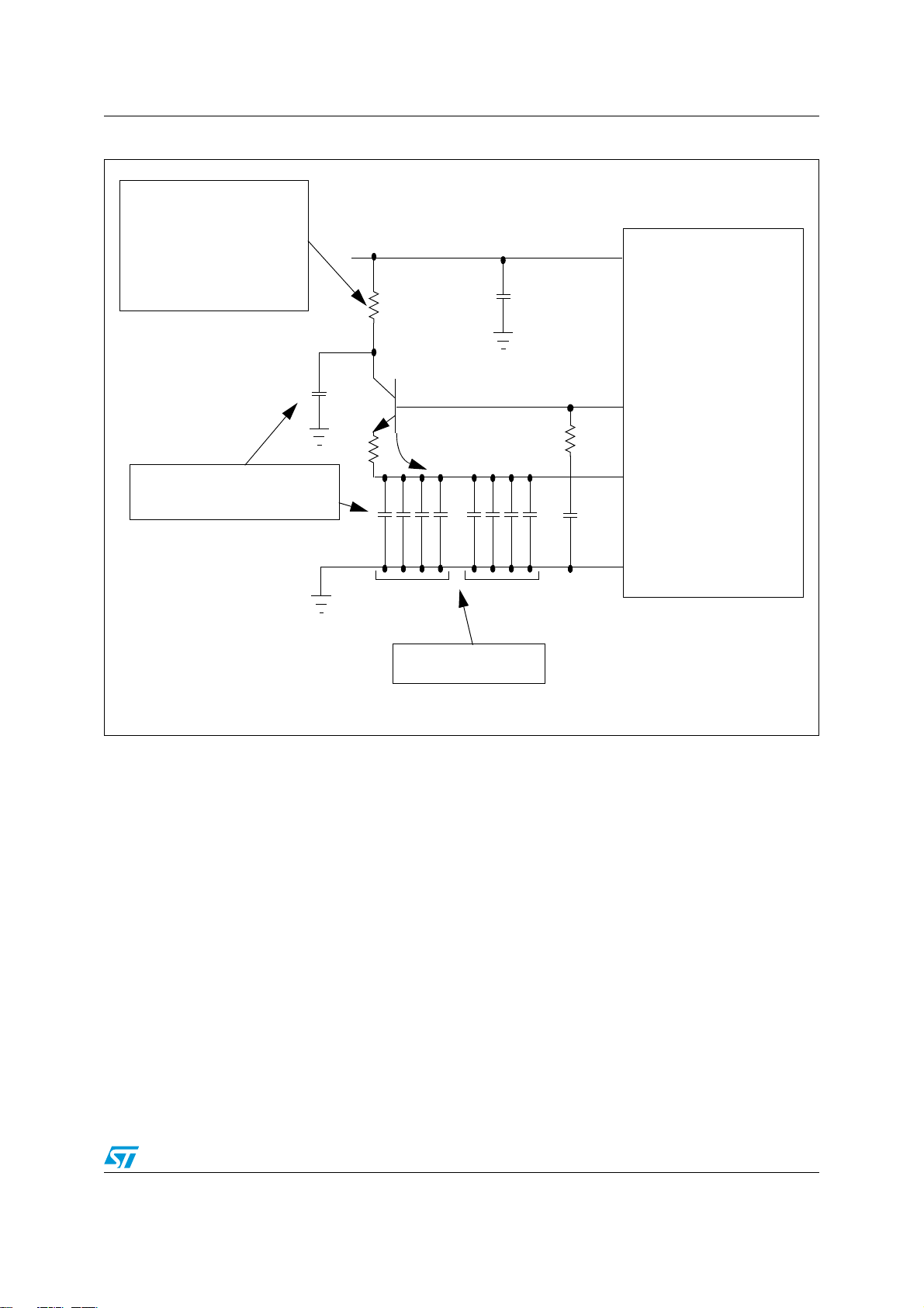
AN4092 Power Management Controller (PMC)
Figure 1. Voltage regulator external components guaranteed configuration 1
2ESISTORMAYORMAYNOTBE
REQUIRED)TDEPENDSONTHE
ALLOWABLEPOWERDISSIPATION
REG
6
$$2%'
2
#
0&8
6
2##4,
B
6
$$
B
OFTHENPNBYPASSTRANSISTOR
DEVICE4HERESISTORMAYBE
USEDTOLIMITTHEINRUSHCUR
RENTATPOWERON
%MITTERANDCOLLECTORCAPACITORS
SHOULDBEMATCHEDSAMETYPE
2
C
4
#
C
#
+EEPPARASITIC
2
E
INDUCTANCEUNDER
N(
EMITTER
6
$$
#
E
#
D
-ANDATORYDECOUPLING
CAPACITORNETWORK
6
33
'!0'2)
Doc ID 023080 Rev 1 9/38
Page 10
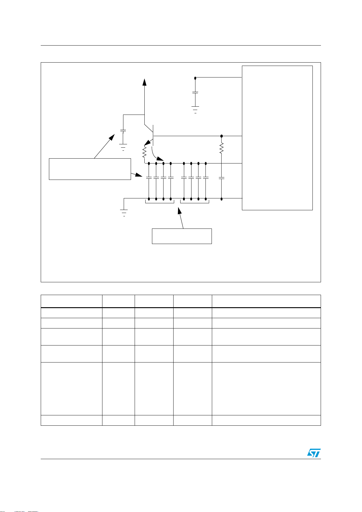
Power Management Controller (PMC) AN4092
Figure 2. Voltage regulator external components guaranteed configuration 2
%MITTERANDCOLLECTORCAPACITORS
SHOULDBEMATCHEDSAMETYPE
6
#
4
#
C
+EEPPARASITIC
INDUCTANCEUNDER
2
E
#
E
N(
EMITTER6$$
#
D
REG
6
$$2%'
2
#
0&8
6
2##4,
B
6
$$
B
6
33
-ANDATORYDECOUPLING
CAPACITORNETWORK
T able 1. External network specification
External component Min. Typ. Max. Notes
T1 NJD2873 or BCP68 only
C
b
C
e
Equivalent ESR of C
capacitors
1.1uF 2.2uF 2.97uF X7R, -50% / +35%
3 x 2.35uF
+ 5uF
e
5mOhm 50mOhm
3 x 4.7uF +
10uF
3 x 6.35uF +
13.5uF
X7R, -50% / +35%
X7R, -50% / +35%
In order to have one cap on each VDD
(EMC rules), depending on the package the
C
d
4 x 50nF 4 x 100nF 7 x 135nF
number of these capacitors may be
increased up to 7x100nF.
700nF is the absolute max allowed: it can
be also split in 12x56nF or 17x47nF.
R
b
9Ohm 10Ohm 11Ohm +/-10%
'!0'2)
10/38 Doc ID 023080 Rev 1
Page 11
AN4092 Power Management Controller (PMC)
Table 1. External network specification (continued)
External component Min. Typ. Max. Notes
C
reg
R
c
R
e
Table 2. Miscellaneous decoupling caps
1.1Ohm 5.6Ohm
0.18Ohm 0.2Ohm 0.22Ohm
10uF
Depending on the 5V regulator impedance,
the required capacitor can go up to 100uF
May or may not be required. It depends on
the allowable power dissipation of T
1
+/-10% The required value can be obtained
by using more resistors in parallel
Supply Quantity Value Notes
VRC33 1 470nF - 2uF Low ESR (<50mOhm)
VSTBY 1 10nF
To be grounded if the Stand-by feature is
not used.
1 100nF
VDDPLL
1 10nF
4 100nF
VDDEHx
Two pairs each side
4 1nF
VDDA 1 10uF To be connected between VDDA and VSSA
VRH 1 10nF
VRL
VSSA
REFBYPC 1 100nF
1.1.6 Inrush current
Since big capacitors need to be charged, a large current can be required when the power is
turned on, to be more precise when the 1.2V regulator is switched on.
A soft-start circuitry is included in the 1.2V regulator but the ramp is only limited to 60-80us
(PVT variation), being ineffective for limiting the inrush current.
As already pointed out in the Section 1.1.4, the resistor on the collector may or may not be
required depending on the allowable power dissipation of the ballast transistor. However the
resistor on the collector can be also very useful in limiting the current necessary to charge
the capacitors during power on.
REFBYPC is not a supply. The external
bypass capacitor must be placed between
REFBYPC pin and GND.
Doc ID 023080 Rev 1 11/38
Page 12
Power Management Controller (PMC) AN4092
Figure 3. Inrush current example - without collector resistor
Figure 4. Inrush current example - with collector resistor
1.1.7 Layout recommendations
The inductance of the heatsink rail of the ballast transistor and the MCU lead to inductance
in the system. The placement of the transistor also affects the inductance, due to the lengths
of the 1.2 V traces (from the emitter to the V
inductances eventually reduce the phase margin jeopardizing the regulator stability.
It is mandatory to keep the parasitic inductance between the emitter and V
than 20nH.
pins) and of the VRCCTL signal: those
DD
pins lower
DD
12/38 Doc ID 023080 Rev 1
Page 13

AN4092 Power Management Controller (PMC)
Use preferably a small plane to distribute VDD with a low parasitic inductance to each pin.
Using of multi-layer printed circuit board (PCB) with a separate layer dedicated to the ground
and another one to the voltages supply is also advised. If the small plane approach is not
possible, try to keep short and wide the traces between the ballast transistor and the micro
and the layout compact to reduce the parasitic.
Figure 5. VDD distribution using a small plane example
9
''
9
''
9
''
6IASTO6
9
''
6$$ISLAND
1-'
%&3
4OKEEPTHEDRAWINGSIMPLEDECOUPLINGCAPSAND
2
E
OTHER0-#NETWORKCOMPONENTSARENOTSHOWN
'!0'2)
Possibly, the ground plane should be adjacent to the VDD island, with a thin dielectric. This
build a good quality HF capacitor. Moat at least 1 to 3 mm between the different power
planes, never overlap them. Use multiple vias to connect to inner layers. This reduce the
inductance, being the vias parasitic inductance in parallel.
Decoupling capacitors are placed as close as possible to the VDD/VSS pair:
● connected to both VDD and VSS pins (closest pins);
● connected to each VDD/VSS pair.
Doc ID 023080 Rev 1 13/38
Page 14

Power Management Controller (PMC) AN4092
For EMC reasons, decoupling capacitors are connected to the VDD and VSS of adjacent
pins. This is illustrated by Figure 6.
Figure 6. Implementation of decoupling Capacitors
6IATO6
33
6IATO6
$$
63&063&$
'OODIMPLEMENTATION
&DS
9
''
6IATO6
33
&DS
6IATO6
33
9
66
9
9
66
''
63&063&$
)MPLEMENTATIONTOBEAVOIDED
'!0'2)
Do not place one or more caps close to the transistor emitter in order to avoid potential
resonant CLC network (emitter cap(s) -> parasitic inductance -> VDD caps).
1.2 External power supply configuration
In this configuration the three voltage levels required are provided externally: VRCCTL can
be left floating, VRC33 becomes the input of the 3.3 voltage and VDD pins/balls must be
connected to the 1.2 V source.
In order to switch off the internal 3.3 voltage regulator, two solutions are possible:
1. VDDREG = GND
Disabling the regulator using this option implies disabling also the Low Voltage Inhibit circuit.
SPC564Axx
2. vrc3p3_shutdown_shadow_bit = 0 (bit 31, least significant bit) in the FLASH_BIU4
register (0xC3F8_802C)
The default value after reset of the volatile register FLASH_BIU4 can be modified by
programming the shadow FLASH location 0x00FF_FE10.
SPC563Mxx
3. V33EN = 0
(g)
g. The internal 3.3 V regulator is always switched on during reset.
14/38 Doc ID 023080 Rev 1
Page 15

AN4092 Power Management Controller (PMC)
V33EN is the least significant bit of the NVUSRO (Non-Volatile User Options Register Array 0). This location is inside the shadow block (0x00FF_FE18).
Please refer to the device RM to get more details on how to program the shadow block.
Caution: Note that a wrong erase/programming of the shadow block may get the device definitively
censored and therefore unusable.
1.2.1 Decoupling
Decoupling network(s) are designed taking in account the external voltage supply
requirements.
1.2.2 External power supply slew rate
Make sure that all power supply ramps are not too fast and in line to what is specified in the
device datasheet. Higher slew rates might cause false ESD trigger.
1.2.3 Power up/down sequencing
There is no power sequencing required among power sources during power up and power
down, in order to operate within specification but use of the following sequence is strongly
recommended when the internal regulator is bypassed:
5 V -> 3.3 V and 1.2 V
This is also the normal sequence when the internal regulator is enabled.
1.3 Mixed configurations
According to the main voltage regulator type, the user can decide to choose mixed
configurations:
■ 1.2V internally regulated with NPN ballast and 3.3 V regulator disabled;
■ 3.3V internally generated and 1.2 V provided externally.
For these cases the same recommendations described in the previous paragraphs are still
valid.
1.4 Low-Voltage-Inhibit (LVI)
The SPC564Axx PMC also implements a low voltage detection circuit that is able to issue
either a reset or an interrupt request to the core. LVI resets and interrupts are only enabled
when the voltage regulator is enabled (VDDREG=5 V). If the user grounds VDDREG
(VDDREG = 0 V) and supplies the voltages externally (1.2 V and 3.3 V), it is also necessary
to provide the LVI monitoring externally.
The PMC_MCR (Module Configuration Register) allows the user to configure which action
an LVI event triggers. By default the PMC is configured to issue a reset. To enable
application to report an LVI event, the reset has to be disabled and the interrupt enabled by
acting on the right bits inside the MCR. Please refer to the product RM to get more details.
Note: The user must make sure that the ISR has finished before the voltage sinks below its
functional specification and this may require an increase in the LVI level
Doc ID 023080 Rev 1 15/38
(h)
.
Page 16

Power Management Controller (PMC) AN4092
1.5 Voltage fine tuning
The PMC_TRIMR (Trimming Register) enables the user to fine tune the voltage of the
regulators and the LVI thresholds.This register can be write protected by setting the
trimming lock bit in the PMC_MCR.
Table 3. Fine tuning parameters
Parameter Min. (V) Default (V) Max (V)
LVI 5V trimming 4.13 4.29 4.43
VREG 3.3V trimming 3.15 3.39 3.60
LVI 3.3V trimming 2.93 3.09 3.23
VREG1.2V trimming 1.12 1.28 1.42
LVI 1.2V trimming 1.0 1.16 1.30
Caution: Fine tuning may end-up in non-guaranteed operating conditions, please refer to the product
datasheet for the maximum operating conditions.
1.6 Stand-by RAM functionality
The SPC564Axx / SPC563Mxx include up to 192 KB of general-purpose SRAM. The first 32
KB of SRAM is powered by its own power supply pin during standby operation.
The Standby mode preserves contents of the standby portion of the memory when the 1.2 V
(VDD) power drops below the level of the standby power supply voltage. There are two
possible supplies for standby: 0.95-1.2 V directly from the VSTBY pin and 2 – 5.5 volts (also
on the VSTBY pin), which enables a standby regulator.
Updates to the standby portion of the SRAM are inhibited during system reset or during
Standby Mode.
1.6.1 SRAM Standby switch
The SRAM Standby Switch provides selection of standby power to the standby SRAM. The
switch selects between the core power supply VDD and an internal regulated voltage
generated from the VSTBY supply.
When VDD falls below 0.95V, the switching occurs and the RAM is on the standby supply. At
the same time, a power down signal is sent to the RAM to power it down to a safe mode
state.
h. Refer to section 1.5: Voltage fine tuning
16/38 Doc ID 023080 Rev 1
Page 17

AN4092 Power Management Controller (PMC)
The standby switch breaks before make, and hence is not shorted Vdd to Vstby during the
transition.
● When the switch sources Vdd_array from Vstby, and Vdd ramps high, the switch
transitions to sourcing Vdd anywhere while 0 < Vdd - Vstby < 0.050V is valid
● When the switch sources Vdd_array from Vdd, the switch is designed to transition to
Vstby when Vstby > Vdd
● The switch works with all ramp rates of Vdd
● The circuit is not drew excessive leakage current if Vdd remains at a mid-level
If VSTBY is not used, it must be connected to ground. When VSTBY is grounded, the switch
is always connected to VDD.
1.6.2 Standby Regulator
The purpose of the regulator is for when VSTBY is in the range of 2V-5.5V. The regulated
output is 1V. When the standby voltage is in the range of 0.95V-1.2V, the regulator is
bypassed and the RAM sees the raw, unregulated standby voltage.
1.6.3 Brown-out Detector
The brown-out detector monitors the standby voltage and sets the BRW flag on the PMC
Configuration and Status Register when the voltage on the VSTBY pin falls to 600 mV. After
reset, this flag comes up asserted and then it can be cleared by software by writing 1 to it.
When the voltage on the VSTBY pin is 0, the brownout detector flag is also 0, regardless of
the voltage on VDD.
1.7 Power dissipation
The total power dissipation depends on the current required on the different supplies. It also
depends on the power configuration. In the single 5V supply configuration, the contributors
are:
1. VDD * IDD
2. VDDA * IDDA
3. VDDREG * IDDREG
4. VDDEHx * IDDEHx
If the internal 3.3V voltage regulator is switched off the contributors are:
1. VDD * IDD
2. VDDA * IDDA
3. VDDREG * IDDREG
4. VRC33 * IDD33
5. VDDEHx * IDDEHx
(i)
(j)
i. Please refer to device errata sheet to check whether or not this feature is available.
j. If the internal 3.3V is switched off but VDDREG is not grounded, there is still a small current consumption due
to the LVI circuitry and the 1.2V regulator.
Doc ID 023080 Rev 1 17/38
Page 18

Power Management Controller (PMC) AN4092
1.7.1 Internal logic power consumption
Most of the logic is powered by the 1.2V. In the worst case, the power that must be
dissipated internally is given by the maximum VDD voltage multiplied by the maximum
current required: VDD
max
* IDD
max
. IDD
normally depends on the operating frequency.
max
1.7.2 Analog power consumption
In the worst case the power required by the ADC that must be dissipated internally is given
by the maximum VDDA voltage multiplied by the maximum current required: VDDA
IDDA
. The analog current consumption does not depend on the system operating
max
max
*
frequency.
1.7.3 Voltage regulator power consumption
The internal 3.3V regulator uses the 5V provided on the VDDREG to generate the 3.3V. The
same voltage is used to supply the 1.2V regulator. The worst case scenario is: VDDREG
* IDDREG
. When disabled but VDDREG is still powered, there is still a small current
max
max
consumption due to the LVI circuitry and the 1.2V regulator. IDDREG does not depend on
the operating frequency.
1.7.4 3.3V power consumption
When in single supply configuration, the 3.3V is generated internally, therefore the current
consumption is already taken in account in the maximum IDDREG.
When the 3.3V is provided externally, the IDD33 current must be taken in account:
VRC33
max
* IDD33
. IDD33 does not depend on the operating frequency.
max
1.7.5 IOs power consumption
This power consumption depends on the application: pad type, load, switching frequency,
voltage and slew rate. The current consumption of the pads is specified in the device
datasheet for a given load and a given frequency. The other cases can be extracted from the
given data assuming a linear behavior. For example, in the table is shown that a slow pad
with 50pF load switching at 4MHz consumes in average 0.5mA. If in the application the pad
is switching only at 20KHz (assuming the same load), the average consumption is 0.5 *
20000 / 4000000 = 2.5uA. Assuming VDDEH = 3.3V, the power is: 3.3 * 2.5 E-6.
1.7.6 Package power dissipation
Once computed all the power requirements, given a operating temperature and package
(and PCB), it is possible to compute whether or not the power can be dissipated in the
package. The limit is the junction temperature; for this family of devices T
Let’s assume that the operating temperature is T
is R
2.63W.
= 19C/W, then the maximum power that can be dissipated is (Tj - Tamb) / R
JA
θ
= 150C.
j
= 100C and the total thermal resistance
amb
θ
JA
=
18/38 Doc ID 023080 Rev 1
Page 19

AN4092 FMPLL and crystal oscillator
2 FMPLL and crystal oscillator
The frequency modulated phase locked loop (FMPLL) allows the user to generate high
speed system clocks from a crystal oscillator or from an external clock generator. The
onchip oscillator is designed to operate in the range 4-40MHz (SPC563Mxx: 4-20MHz). The
frequency modulation is register programmable (frequency and depth). The clock quality
module (CQM) provides loss-of-clock detection for the FMPLL reference and output clocks
comparing these with the internal RC reference
the FMPLL has achieved frequency lock and continuously monitors lock status to report
loss-of-lock conditions.
The FMPLL is powered through the VDDPLL/VSSPLL supply couple while the onchip
oscillator is powered by the internal 3.3V regulator (or external 3.3V supply).
Figure 7. System clock diagram
(k)
. The lock detection circuitry reports when
2.1 Crystal oscillator and external circuitry
The crystal oscillator circuit is designed and used to provide reference clock to the PLL.
Input to the circuit is a sinusoidal input generated by a crystal with an amplifier. Output is a
square wave which is used as a reference clock to the PLL.
The type of oscillator is a Pierce CMOS crystal one. This oscillator, however, has an
Automatic Level Controller where the amount of current sourced into the amplifier is
inversely proportional to the amplitude of the input signal EXTAL. The EXTAL and XTAL
signals are then fed to inputs of a comparator to generate a square-wave signal.The crystal
oscillator may provide a reference clock to the FMPLL.
k. The internal RC oscillator cannot be used as system clock.
Doc ID 023080 Rev 1 19/38
Page 20

FMPLL and crystal oscillator AN4092
Figure 8. Oscillator
9''3//
9GGV\Q
(;7$/
;7$/B,Q
2.1.1 External circuitry
The external circuitry normally consists of:
● The crystal
● Two load capacitors
● Serial resistor (optional)
The bias resistor is not needed because it is internally implemented.
The maximum value of the total load capacitance is given by the following table:
$/&
,ELDV
5I
;7$/
;7$/B2XW
'!0'2)
Table 4. Crystal total load capacitance
XTAL load capacitance Min. (pF) Max (pF)
4MHz 5 30
8MHz 5 26
12 MHz 5 23
16 MHz 5 19
20 MHz 5 16
40 MHz 5 8
(l)
The circuitry design may need also to take in account parasitic capacitance.
l. This value is determined by the crystal manufacturer and board design. For 4 MHz to 40 MHz crystals specified
for this PLL, load capacitors should not exceed these limits.
20/38 Doc ID 023080 Rev 1
Page 21

AN4092 FMPLL and crystal oscillator
2.1.2 Recommended crystals
The following quartzes have been characterized (reports are available on demand):
● NX8045GB 4MHz
● NX5032GA 8MHz
● NX3225GA 16MHz
● NX5032GA 40MHz (SPC564A only)
2.2 Crystal or external reference
The configuration pin PLLREF configures the FMPLL clock reference at reset:
● Asserted - Indicates that the reference clock comes from the crystal oscillator
● Negated - Indicates that the reference clock comes from the external clock generator.
In this case the external clock source must be connected to the EXTAL pin while XTAL
must be grounded.
Assertion or negation of the PLLREF
and kept stable for the whole reset duration.
Note: PLLCFG1 (SPC564Axx BGA324 only) has no PLL configuration functionality anymore. The
name has been kept for legacy reasons.
(m)
must be done at the beginning of the reset cycle
2.3 Bypass mode or normal mode
In the bypass mode the FMPLL is completely bypassed and the system clock is driven
either from either the crystal oscillator or by an external clock generator connected to the
EXTAL pin. Bypass mode is the default mode at reset.
In the normal mode the FMPLL receives an input clock frequency from either the crystal
oscillator or by an external clock generator and multiplies the frequency to create the FMPLL
output clock.
2.4 Ramp up
As already mentioned, the default system clock after reset is derived from the oscillator.
During ramp-up, it is not desirable to set the FMPLL to jump directly to full operating
frequency. The frequency can be stepped, with delays to allow the power supply to settle.
For example, the target operating frequency of 150MHz (SPC564Axx only) can be reached
in three steps: first to 40MHz, then 80MHz and finally 150MHz.
m. Refer to the Chapter 3: Configuration pins and unused IOs for more details.
Doc ID 023080 Rev 1 21/38
Page 22

FMPLL and crystal oscillator AN4092
63&0
$ECOUPLINGCAPACITOR
#
#
9LDVWR*1'
9LDVWR*1'
&U\VWDO
*URXQGSODWH
#$
9LDVWR9
''
9
''3//
9
663//
;7$/
(;7$/
&U\VWDOSDFNDJH
VROGH
UHGWR*1'
63&$
'!0'2)
2.5 Layout recommendations
● Keep the area of the oscillator circuit as compact as possible, keep tracks very short;
● Avoid any track crossing the oscillator area, also considering inner layers between the
components and the ground plane;
● Keep the routing on one layer;
● Create an island for the oscillator ground on the top layer;
● Open all the inner layers in correspondence of the oscillator to reduce capacitance;
● Surround the oscillator area on component side with a GND guard, do not fill the area
with ground. To be effective, the guard trace must be grounded by vias every a short
lenght (< wavelenght / 20, with reference at the higher frequency present);
● Use robust SMT pads for components in crystal oscillator, short track lengths for all
signals.
Figure 9. PCB layout example for SPC563Mxx / SPC564Axx
22/38 Doc ID 023080 Rev 1
Page 23

AN4092 Configuration pins and unused IOs
3 Configuration pins and unused IOs
In the SPC564Axx / SPC563Mxx there are many configuration pins, they allow to choose
the boot mode, the clock reference and the weak pull-up/pull-down configuration:
● BOOTCFG0 (SPC564Axx only), BOOTCFG1
● PLLREF
● WKPCFG
● RSTCFG (SPC564Axx only)
For legacy reasons, PLLCFG1 is still described in the documentation but there is no
configuration functionality assigned to this pin any longer.
After the reset those pins can be used as GPIO or any of the other functions available.
3.1 Boot modes (SPC564Axx)
BOOTCFG0 and BOOTCFG1 allow the selection of the boot mode. In the QFP176 package
only BOOTCFG1 is available outside while BOOTCFG0 is pulled low internally.
Table 5. Boot modes
BOOTCFG[0:1] Boot Mode Name
00 Internal boot (from FLASH)
01 Serial boot (eSCI / FlexCAN)
10 External boot
11 Reserved
By default both signals are pulled down after reset. If needed, BOOTCFG pins must be
pulled high to VDDEH6. The reset controller latches the value on the BOOCFG[0:1] input to
the SIU_RSR (Reset Status Register) four clock cycles prior to the negation of RSTOUT.
The BAM reads the BOOTCFG status from the SIU_RSR and acts accordingly.
Boot from external bus interface is obviously possible only on the BGA324 package.
3.2 Boot modes (SPC563Mxx)
BOOTCFG1 allows the selection of the boot mode:
■ BOOTCFG = 0, internal boot (form FLASH)
■ BOOTCFG = 1, serial boot (eSCI / FlexCAN)
BOOTCFG1 is pulled down after reset by default.
3.3 Clock reference
As described in the section Section 2.2: Crystal or external reference, the PLLREF pin
determines the source of the reference clock, either crystal or external at the negation of the
/RSTOUT. During assertion of the /RSTOUT, the system clock switches to the input
Doc ID 023080 Rev 1 23/38
Page 24

Configuration pins and unused IOs AN4092
specified by the PLLREF pin. The value on the PLLREF pin must be kept constant during
reset to avoid transients in the system clock.
3.4 Weak pull configuration
The signal on the WKPCFG pin determines whether specified eTPU and eMIOS pins are
connected to weak pull up or weak pull down devices at reset (see the Signal Description
chapter in the Reference Manual for the eTPU and eMIOS pins that are affected by
WKPCFG). For all reset sources except the Software External Reset, the WKPCFG pin is
applied at the assertion of the internal reset signal (assertion of RSTOUT). If the WKPCFG
signal is logic high at this time, pull up devices is enabled on the eTPU and eMIOS pins. If
the WKPCFG signal is logic low at the assertion of the internal reset signal, pull down
devices are enabled on those pins. The value on WKPCFG must be held constant during
reset to avoid oscillations on the eTPU and eMIOS pins caused by switching pull up/down
states. The final value of WKPCFG is latched four clock cycles before the negation of
RSTOUT. After reset, software may modify the weak pull up/down selection for all I/O pins
through the PCR registers in the SIU.
3.5 RSTCFG (SPC564Axx only)
RSTCFG is used to enable or disable the PLLREF and the BOOTCFG[0:1] configuration
signals:
● 0: Get configuration information from BOOTCFG[0:1] and PLLREF
● 1: Use default configuration of booting from internal flash with crystal clock source
Note: For the 176-pin QFP package RSTCFG is always 0, so PLLREF and BOOTCFG signals are
used.
RSTCFG pin allows, for example, to select the most common configuration without the need
of having pulling up/down on several pins.
3.6 Unused I/Os
With respect to power consumption, there is no particular recommendation for unused I/Os:
both input and output buffers are disabled after reset. However, from the EMC perspective, it
is always desirable to tie unused pins to ground or supply voltage, also through internal pullup/down resistors (enabled by default).
24/38 Doc ID 023080 Rev 1
Page 25

AN4092 ADC
4 ADC
The goal of this chapter is to provide hints on how to dimension correctly the external ADC
circuitry in order to reduce errors and, at the same time, to protect the ADC inputs.
Figure 10. Simplified ADC circuitry
%84%2.!,#)2#5)4
3OURCE &ILTER
2
S
6
A
2
F
#
F
).4%2.!,#)2#5)43#(%-%
6
$$!
2
SW
#
P
#
S
'!0'2)
The Figure 10 shows a simplified scheme of the external and internal circuit.
Table 6. SPC564Axx / SPC563Mxx ADC parameters
Parameter Min. Nominal Max
C
p
R
sw
C
(single ended) - - 0.8pF
s
C
(differential) - - 1.3pF
s
ADC clock frequency - - 16MHz
- - 12pF
-8KOhm
21KOhm
(3 sigma, 150C)
Sampling time (ADC
clocks)
2- 128
12bit single ended
conversion time (ADC
-14-
clocks)
12bit differential
conversion time (ADC
-13-
clocks)
Residual voltage on
sample capacitor
1.25V - 3.75V
The external analogue source can be represented as a voltage source with its impedance
(R
). Then it is a common practice to put an RC circuit to filter the analogue source; in
s
addition R
can be also useful as current limiter in case of overvoltage.
f
Doc ID 023080 Rev 1 25/38
Page 26

ADC AN4092
The internal circuitry can be represented by:
● C
● R
● C
The first constraint comes from the current limitation. R
, pin capacitance, including other parasitic capacitance;
p
, switching resistance, including the multiplexer and the sampling switch resistance;
sw
, the sampling capacitance.
s
must be chosen to limit the injection
f
current:
Equation 1
RsR+
V
amaxVDDA
------------ ------------- --------------- ------------ ---- -
≥
f
I
INJmax
0.5+()–
Equation 2
Being V
V
------------- ------------- ---
R+
R
+ 0.5 the positive clamping voltage and -0.3 the negative clamping voltage.
DDA
≥
s
f
amin
I
INJmin
0.3–
The next condition comes from the analogue source bandwidth f
cut the noise. Being f
the cut-off frequency of the filter, we have:
f
Equation 3
1
------------ ------------ -------------
f
f
2πR
fCfCp
==
f
+()
0
. The filter are designed to
0
On the other hand, to prevent aliasing, according to the Nyquist theorem, the frequency f
be at least 2f
:
0
Equation 4
1
---------------------- -
+()
T
sTc
Where T
is the sampling time and Tc is the conversion time. Ts is configurable (2, 8, 64, 128
s
ADC clock cycles), while T
1
f
-------=
N
T
N
is 13 ADC clock cycles for a differential conversion and 14 for a
c
single ended conversion.
Finally T
26/38 Doc ID 023080 Rev 1
is chosen to allow the charge sharing to be complete.
s
2f
N
1
------------ ------------- -------- -=≥=
0
πR
fCfCp
+()
Page 27

AN4092 ADC
When the conversion switch closes, the charges between the capacitors are shared,
producing a new voltage that depends upon the initial voltages and the size of the
capacitors. This process takes places at the rate of the internal ADC time constant (R
swCs
).
At the same time the charge share voltage starts to recover towards the actual sample
voltage at the rate of the external RC time constant R
f(Cf+Cp
). Even if the two processes are
interdependent, they can be treated as separated, as long as the internal time constant is
much smaller than the external one.
Being V
the sample voltage and V1 the voltage after the charge sharing:
s
Equation 5
CfCp+()VsCfCpC
=
++()V
s
Therefore:
Equation 6
V
1
C
++
fCpCs
V
s
CfCp+()
------------ ------------ --------
=
happening with an exponential law which time constant is:
Equation 7
1
=
τ
1RswCs
Then the voltage V
recovers exponentially towards Vs with the time constant:
1
Equation 8
τ
2RfCfCp
+()=
Normally the latter is much larger than the first. This gives us the final constraint:
Doc ID 023080 Rev 1 27/38
Page 28

ADC AN4092
Equation 9
τ1τ2T
««
s
However the last constraint can’t be always fulfilled. For example when the time constant
R
f(Cf+Cp
to reduce the resistor R
) has to be big in order to filter out very low frequencies. In this case it is preferable
(as long as the current limitation constraint is kept) and increase Cf:
f
it results in a very small drop due to the charge sharing and eventually a small or negligible
error.
EXAMPLE 1
Let’s assume that:
● V
● R
● f
Using the Equation 1:
= 12V
amax
= 100Ohm
s
= 100KHz
0
Let’s choose R
= 2.2KOhm.
f
Then, from the Equation 3:
Let’s choose C
= 680pF.
f
Then, from the Equation 4:
12 5.5–
R
------------ -------- - 100– 2KΩ≅≥
f
310
⋅
------------ ------------ --------------- ------------- ------
C
f
2π100 10
T
sTc
------------ ------------- ---=+ 5μ s=
200 103⋅()
3–
1
3
2.2 103⋅()⋅
723pF==
1
Clocking the ADC at its maximum frequency (16MHz):
28/38 Doc ID 023080 Rev 1
Page 29

AN4092 ADC
Ts80 14 66ADCclockcycles=–=
Let’s choose Ts = 64 and continuos conversion.
The external RC time constant R
f(Cf+Cp
) is 1.496us, therefore Ts is about 3 times that
constant, meaning that the second exponential transient is not really over. However, the
voltage drop due to the charge share is only (Equation 6: ) 4.41mV (worst case
to a negligible error (being T
= 3 x time constant).
s
(n)
), leading
EXAMPLE 2
Let’s assume that:
● V
● R
● f
Using the Equation 1:
Let’s choose R
Then, from the Equation 3:
= 24V
amax
= 100Ohm
s
= 50Hz
0
= 6.2KOhm.
f
R
f
24 5.5–
------------ -------- - 100– 6KΩ≅≥
310
⋅
3–
1
----------- ------------- --------------- --
Let’s choose C
= 470nF.
f
C
f
2π50 6.2 10
⋅()
513nF==
3
In this case, being the signal slow, we can simply choose the maximum sampling time: T
128. Then the ADC can be triggered by an internal timer to meet the Nyquist requirement f
= 2f
.
0
The capacitance C
is much bigger than the internal one, leading to a negligible voltage drop
f
and hence basically no conversion errors due to the charge sharing, hence allowing
potentially even smaller sampling times, reducing the overall conversion time.
n. The worst case is 3.75V, difference between the sample voltage and the residual voltage on the sample
capacitance.
Doc ID 023080 Rev 1 29/38
=
s
N
Page 30

ADC AN4092
4.1 Alternative approach
In some cases the filtering using the RC might not be effective. Instead of using costly active
external analogue filters, an internal digital filtering can be implemented using the
decimation filter. The approach is the following:
1. Choose a simple RC outside filter which cut-off frequency is much higher than the
interested bandwidth of the signal, including the noise.
2. Oversample the signal, potentially sampling at the maximum frequency allowed by the
ADC
3. Filter the noise out using the IIR / FIR feature
4. Decimate
For example this approach can be very effective to threat knock sensors outputs, in which
the big noise cannot be easily filtered out using a simple RC.
30/38 Doc ID 023080 Rev 1
Page 31

AN4092 Reset
5 Reset
In the SPC564Axx / SPC563Mxx devices two reset related pins are implemented:
● /RESET
● /RSTOUT
being respectively the reset input and the reset output.
5.1 /RESET
The /RESET pin is an active low input. The RESET pin is asserted by an external device
during a power-on or external reset. The internal reset signal asserts only if the RESET pin
asserts for 10 clock cycles.
Assertion of the /RESET pin while the device is in reset causes the reset cycle to start over.
The /RESET pin has a glitch detector which detects spikes greater than two clocks in
duration that fall below the switch point of the input buffer logic of the VDDEH input pins. The
switch point lies between the maximum VIL and minimum VIH specifications for the VDDEH
input pins.
5.2 /RSTOUT
The /RSTOUT pin is an active low output that uses a push/pull configuration. The /RSTOUT
pin is driven to the low state by the MCU for all internal and external reset sources.
Depending on the PLL configuration, External Reference or Crystal Mode, the /RSTOUT pin
is asserted after a different delay depending on the reset source
sampling of the configuration pins.
The /RSTOUT pin can also be asserted by a write to the SER bit of the System Reset
Control Register (SIU_SRCR).
5.3 Reset source description
The table below summarizes the reset sources and their effect on the system.
(o)
, plus four cycles for
o. Refer to the device reference manual.
Doc ID 023080 Rev 1 31/38
Page 32

Reset AN4092
T a ble 7. Reset source description
Registers
Reset
source
SRAM JTAG
(1)
(including
(2)
PMC
(3)
,
PLL, etc.)
Rando
m
content
POR/LVI
/
XX
Retenti
on not
reliable
ER / LLR /
LCR /
WTDR /
JTAG
Reset /
Content
unaffect
ed
Not
affected
(6)
X
SSR
SER
Content
unaffect
ed
Not
affected
Not
affected
(4)
OSC
Not
affected
Not
affected
Not
affected
PORT
PINBAM
Reset
state
as per
signal
proper
ties
table
(5)
Reset
state
as per
signal
proper
ties
table
(7)
Not
affect
ed
Exec
uted
Exec
uted
Not
exec
uted
WKPCFG,
PLLREF,
BOOTCFG
Sampled
Sampled
Not Sampled
Factory
trimming
Tr im mi n g
reloaded
from Flash
Tr im mi n g
kept
Tr im mi n g
kept
Shadow
information
(NVUSR0,
Lock
Registers,
etc.)
Reloaded from
Flash
Reloaded from
Flash
Not reloaded
from Flash
1. POR: Power-on Reset / LVI: Low Voltage Inhibit / ER: External Reset / LLR: Loss of Lock Reset / LCR: Loss of Clock Reset
/ WTDR: Watchdog Timer/Debug Reset / SSR: Software System Reset / SER: Software External Reset
2. JCOMP is used to reset JTAG Controller
3. Including MCR register
4. Provided that the supply voltages are within the limits
5. Refer to RM / DS
6. RAM content unaffected (CAN message buffer, ETPU memories, etc.)
7. Refer to RM / DS
32/38 Doc ID 023080 Rev 1
Page 33

AN4092 Reset
5.4 Reset circuitry example
Figure 11. Reset circuitry example
0DQXDO
5HVHW
9ROWDJH
UHJXODWR
9
52
U
9&&
05
X3UHVHW
FLUFXLW
966
-7$*
567
5(6(
567287
9''(+
7
63&$[[
63&0[[
567,1
([WGHYLFH
9&&
'!0'2)
Doc ID 023080 Rev 1 33/38
Page 34

Previous recommended PMC network configurations AN4092
Appendix A Previous recommended PMC network
configurations
Figure 12 shows an old recommended configuration that was proven to be unstable in some
corner cases, especially with NJD2873.
Figure 12. SPC563Mxx configuration/SPC564Axx configuration
Resistor may or may not be
required. It depends on the
allowable power dissipation
of the npn bypass transistor
device.
V
DDREG
1.1–5.6Ω
6.8-10μF
Emitter and collector capacitors
(6.8 μF and 10 μF) should be
matched (same type) and ESR
should be lower than 200 mΩ.
4 × 6.8 μF4 × 220 nF
Notes:
1. The V
2. The bypass transistor MUST be operated out of its saturation region.
capacitor and resistor required.
RCCTL
10 μF
V
RCCTL
15 Ω
V
DD
680nF
V
SS
Mandatory decoupling
capacitor network
MCU
GAPGRI00160
However, when the ballast transistor in use is BCP68, this configuration is still safe to use
with SPC563Mxx. With a small modfification to the snubber network on the base (see
Figure 13), it is safe with NJD2873 too.
The configuration shown in Figure 12 must never be used in any SPC564Axx design.
Note: Figure 12 is not present in last versions of Datasheet and Reference manual as it is
outdated (for further information see Section Appendix B: Further information).
34/38 Doc ID 023080 Rev 1
Page 35

AN4092 Previous recommended PMC network configurations
Figure 13. Alternate SPC563Mxx configuration
Resistor may or may not be
required. It depends on the
allowable power dissipation
of the npn bypass transistor
device.
V
DDREG
1.1–5.6Ω
6.8-10μF
10 μF
Emitter and collector capacitors
(6.8 μF and 10 μF) should be
matched (same type) and ESR
should be lower than 200 mΩ.
4 × 6.8 μF4 × 220 nF
Notes:
1. The V
capacitor and resistor required.
RCCTL
2. The bypass transistor MUST be operated out of its saturation region.
V
RCCTL
6.8 Ω
V
DD
2.2 μF
V
SS
Mandatory decoupling
capacitor network
MCU
GAPGRI00161
Doc ID 023080 Rev 1 35/38
Page 36

Further information AN4092
Appendix B Further information
B.1 Reference documents
● 32-bit MCU family built on the embedded Power Architecture
SPC564A74L, SPC564A80B4, SPC564A80L7, Doc ID 15399)
● 32-bit MCU family built on the embedded Power Architecture
15117)
● 32-bit Power Architecture
®
based MCU for automotive powertrain applications
(SPC563M64, Doc ID 14642
● SPC563M64xx - 32-bit Power Architecture
®
based MCU with up to 1.5 Mbyte Flash
and 111 Kbyte RAM memories (RM0015, Doc ID 14499)
®
(SPC564A74B4,
®
(RM0029, Doc ID
36/38 Doc ID 023080 Rev 1
Page 37

AN4092 Revision history
Revision history
Table 8. Document revision history
Date Revision Changes
02-May-2012 1 Initial release.
Doc ID 023080 Rev 1 37/38
Page 38

AN4092
U
D
W
D
W
S
O
U
T
R
G
A
Y,
D
E
G
Please Read Carefully:
Information in this document is provided solely in connection with ST products. STMicroelectronics NV and its subsidiaries (“ST”) reserve the
right to make changes, corrections, modifications or improvements, to this document, and the products and services described herein at any
time, without notice.
All ST products are sold pursuant to ST’s terms and conditions of sale.
Purchasers are solely responsible for the choice, selection and use of the ST products and services described herein, and ST assumes no
liability whatsoever relating to the choice, selection or use of the ST products and services described herein.
No license, express or implied, by estoppel or otherwise, to any intellectual property rights is granted under this document. If any part of this
document refers to any third party products or services it shall not be deemed a license grant by ST for the use of such third party products
or services, or any intellectual property contained therein or considered as a warranty covering the use in any manner whatsoever of such
third party products or services or any intellectual property contained therein.
NLESS OTHERWISE SET FORTH IN ST’S TERMS AND CONDITIONS OF SALE ST DISCLAIMS ANY EXPRESS OR IMPLIE
ARRANTY WITH RESPECT TO THE USE AND/OR SALE OF ST PRODUCTS INCLUDING WITHOUT LIMITATION IMPLIE
ARRANTIES OF MERCHANTABILITY, FITNESS FOR A PARTICULAR PURPOSE (AND THEIR EQUIVALENTS UNDER THE LAW
F ANY JURISDICTION), OR INFRINGEMENT OF ANY PATENT, COPYRIGHT OR OTHER INTELLECTUAL PROPERTY RIGHT.
NLESS EXPRESSLY APPROVED IN WRITING BY TWO AUTHORIZED ST REPRESENTATIVES, ST PRODUCTS ARE NO
ECOMMENDED, AUTHORIZED OR WARRANTED FOR USE IN MILITARY, AIR CRAFT, SPACE, LIFE SAVING, OR LIFE SUSTAININ
PPLICATIONS, NOR IN PRODUCTS OR SYSTEMS WHERE FAI LURE OR MALFUNCTION MAY RESULT IN PERSONAL INJUR
EATH, OR SEVERE PROPERTY OR ENVIRONMENTAL DAMAGE. ST PRODUCTS WHICH ARE NOT SPECIFIED AS "AUTOMOTIV
RADE" MAY ONLY BE USED IN AUTOMOTIVE APPLICATIONS AT USER’S OWN RISK.
Resale of ST products with provisions different from the statements and/or technical features set forth in this document shall immediately void
any warranty granted by ST for the ST product or service described herein and shall not create or extend in any manner whatsoever, any
liability of ST.
The ST logo is a registered trademark of STMicroelectronics. All other names are the property of their respective owners.
ST and the ST logo are trademarks or registered trademarks of ST in various countries.
Information in this document supersedes and replaces all information previously supplied.
© 2012 STMicroelectronics - All rights reserved
STMicroelectronics group of companies
Australia - Belgium - Brazil - Canada - China - Czech Republic - Finland - France - Germany - Hong Kong - India - Israel - Italy - Japan -
Malaysia - Malta - Morocco - Philippines - Singapore - Spain - Sweden - Switzerland - United Kingdom - United States of America
www.st.com
38/38 Doc ID 023080 Rev 1
 Loading...