How it Works
Log In / Sign Up
Buy Points
How it Works
FAQ
Contact Us
Questions and Suggestions
Users
Datasheet
Loading...
A
AN3967
AN3968
AN3969
AN3969K
AN3970
AN3972
AN3973
AN3980
AN3981
AN3983
AN3984
AN3985
AN3986FBP
AN3986FHP
AN3988
AN3990
AN3991
AN3992
AN3994
AN3995
AN3996
AN3997
AN3998
AN4006
AN4007
AN4009
AN4013
AN4014
AN4015
AN4016
AN4023
AN4027
AN4030
AN4032
AN4035
AN4038
AN4041
AN4043
AN4044
AN4046
AN4050
AN4054
AN4055
AN4057
AN4058
AN4061
AN4062
AN4065
AN4068
AN4069
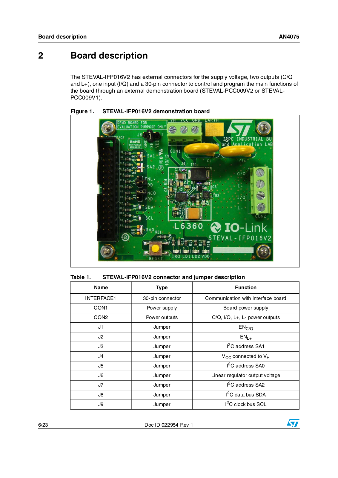
AN4075
AN4086
AN4088
AN4092
AN4099
AN4104
AN4110
AN4112
AN4118
AN4123
AN4125
AN4127
AN4128
AN413
2
AN4133
AN4144
AN417
2
an419
AN420
2
AN421
AN4250
AN4250S
AN431
AN432
AN437
AN439
AN440
AN441
AN442
AN4505
AN4506
AN453
AN4558
AN4558S
AN469
AN471
AN483
AN4839
AN485
AN4869
AN487
AN495
AN5010
AN502
AN5071
2
AN5095K
AN5130
AN5138NK
AN5150N
AN5151
Loading...
Loading...
Nothing found
AN4075
APPLICATION NOTE (ST)
23 pgs
419.24 Kb
0
Table of contents
Loading...
Datasheet AN4075 APPLICATION NOTE (ST)
...
Datasheet APPLICATION NOTE (ST)
Download
Specifications and Main Features
Frequently Asked Questions
User Manual
Download
Loading...
+
hidden pages
Unhide
You need points to download manuals.
1 point = 1 manual.
You can buy points or you can get point for every manual you upload.
Buy points
Upload your manuals


")