

Page 1

AN4013
Application note
STM32F1xx, STM32F2xx, STM32F4xx, STM32L1xx timer overview
1 Introduction
This document:
● presents an overview of the timer peripherals in the STM32F1xx, STM32F2xx,
STM32F4xx and STM32L1xx microcontroller families,
● describes the various modes and specific features of the timers, such as clock sources,
● explains how to use the available modes and features,
● explains how to compute the time base in each configuration,
● describes the timer synchronization sequences and the advanced features for motor
control applications, in addition to the basic timer modes.
For each mode, typical configurations are presented and examples of how to use the modes
are provided.
In the rest of this document (unless otherwise specified), the term STM32xx is used to refer
to STM32F1xx, STM32F2xx, STM32F4xx and STM32L1xx microcontroller families.
February 2012 Doc ID 022500 Rev 1 1/27
www.st.com
Page 2

Contents AN4013
Contents
1 Introduction . . . . . . . . . . . . . . . . . . . . . . . . . . . . . . . . . . . . . . . . . . . . . . . . 1
2 Overview . . . . . . . . . . . . . . . . . . . . . . . . . . . . . . . . . . . . . . . . . . . . . . . . . . 3
3 Basic timer modes . . . . . . . . . . . . . . . . . . . . . . . . . . . . . . . . . . . . . . . . . . 6
3.1 Clock input sources . . . . . . . . . . . . . . . . . . . . . . . . . . . . . . . . . . . . . . . . . . 6
3.1.1 Internal clock . . . . . . . . . . . . . . . . . . . . . . . . . . . . . . . . . . . . . . . . . . . . . . 6
3.1.2 External clock . . . . . . . . . . . . . . . . . . . . . . . . . . . . . . . . . . . . . . . . . . . . . 6
3.2 Time base generator . . . . . . . . . . . . . . . . . . . . . . . . . . . . . . . . . . . . . . . . . 7
3.3 Timer input capture mode . . . . . . . . . . . . . . . . . . . . . . . . . . . . . . . . . . . . . 9
3.4 Timer output compare mode . . . . . . . . . . . . . . . . . . . . . . . . . . . . . . . . . . 10
3.5 Timer PWM mode . . . . . . . . . . . . . . . . . . . . . . . . . . . . . . . . . . . . . . . . . . 12
3.6 Timer one pulse mode . . . . . . . . . . . . . . . . . . . . . . . . . . . . . . . . . . . . . . . 13
4 Timer synchronization . . . . . . . . . . . . . . . . . . . . . . . . . . . . . . . . . . . . . . 14
4.1 Timer system link . . . . . . . . . . . . . . . . . . . . . . . . . . . . . . . . . . . . . . . . . . . 14
4.2 Master configuration . . . . . . . . . . . . . . . . . . . . . . . . . . . . . . . . . . . . . . . . . 14
4.3 Slave configuration . . . . . . . . . . . . . . . . . . . . . . . . . . . . . . . . . . . . . . . . . . 15
5 Advanced features for motor control . . . . . . . . . . . . . . . . . . . . . . . . . . 16
5.1 Signal generation . . . . . . . . . . . . . . . . . . . . . . . . . . . . . . . . . . . . . . . . . . . 16
5.2 Specific features for motor control applications . . . . . . . . . . . . . . . . . . . . 18
5.2.1 Complementary signal and dead time feature . . . . . . . . . . . . . . . . . . . . 18
5.2.2 Break input . . . . . . . . . . . . . . . . . . . . . . . . . . . . . . . . . . . . . . . . . . . . . . . 19
5.2.3 Locking mechanism . . . . . . . . . . . . . . . . . . . . . . . . . . . . . . . . . . . . . . . . 20
5.2.4 Specific features for feedback measurement . . . . . . . . . . . . . . . . . . . . . 20
6 Specific applications . . . . . . . . . . . . . . . . . . . . . . . . . . . . . . . . . . . . . . . . 24
6.1 Infrared application . . . . . . . . . . . . . . . . . . . . . . . . . . . . . . . . . . . . . . . . . . 24
6.2 3-phase AC and PMSM control motor . . . . . . . . . . . . . . . . . . . . . . . . . . . 24
6.3 Six-step mode . . . . . . . . . . . . . . . . . . . . . . . . . . . . . . . . . . . . . . . . . . . . . 24
7 Revision history . . . . . . . . . . . . . . . . . . . . . . . . . . . . . . . . . . . . . . . . . . . 26
2/27 Doc ID 022500 Rev 1
Page 3

AN4013 Overview
2 Overview
STM32 devices use various types of timers, with the following features for each:
● General purpose timers are used in any application for output compare (timing and
delay generation), one-pulse mode, input capture (for external signal frequency
measurement), sensor interface (encoder, hall sensor)...
● Advanced timers: these timers have the most features. In addition to general purpose
functions, they include several features related to motor control and digital power
conversion applications: three complementary signals with deadtime insertion,
emergency shut-down input.
● One or two channel timers: used as general purpose timers with a limited number of
channels.
● One or two channel timers with complementary output: same as previous type, but
having a deadtime generator on one channel. This allows having complementary
signals with a time base independent from the advanced timers.
● Basic timers have no input/outputs and are used either as timebase timers or for
triggering the DAC peripheral.
Ta bl e 1 summarizes the STM32 family timers.
Ta bl e 2 presents a general overview of timer features.
Doc ID 022500 Rev 1 3/27
Page 4
Overview AN4013
Table 1. STM32 family timers
STM32F101/102/
Timer type
103/105/107
families
TIM1 TIM1
Advanced
TIM8
TIM2 TIM2 TIM2
TIM3 TIM3 TIM3 TIM3
16-bit
General
purpose
TIM4 TIM4 TIM4 TIM4
TIM5 TIM5
32-bit
TIM6 TIM6 TIM6 TIM6
Basic
TIM7 TIM7 TIM7 TIM7
TIM10
TIM11
1-channel
TIM13 TIM13
TIM14 TIM14
TIM9
2-channel
TIM12 TIM12
1-channel with one
complementary output
STM32F100
family
TIM15
STM32L1
family
STM32F2 and
STM32F4
families
TIM1
TIM8
TIM2
TIM5
TIM10 TIM10
TIM11 TIM11
TIM13
TIM14
TIM9 TIM9
TIM12
2-channel with one
complementary output
TIM16
TIM17
4/27 Doc ID 022500 Rev 1
Page 5

AN4013 Overview
Table 2. Timer features overview
Synchronization
Timer type
Counter
resolution
Advanced 16 bit
General purpose
16 bit
32 bit
Counter type DMA Channels
(1)
up, down and
center aligned
up, down and
center aligned
Ye s 4 3 Ye s Ye s
Ye s 4 0 Ye s Ye s
Comp.
channels
Master
config.
Slave
config.
Basic 16 bit up Yes 0 0 Yes No
1-channel 16 bit up No 1 0
Ye s ( O C
signal)
No
2-channel 16 bit up No 2 0 Yes Yes
1-channel with one
complementary
output
16 bit up Yes 1 1
Ye s ( O C
signal)
No
2-channel with one
complementary
16 bit up Yes 2 1 No Yes
output
1. TIM2 and TIM5 are 32-bit counter resolution in the STM32F2 and STM32F4 families.
Doc ID 022500 Rev 1 5/27
Page 6

Basic timer modes AN4013
3 Basic timer modes
Basic timers can be programmed to work in one of the following configurations.
3.1 Clock input sources
The timer can be synchronized by several clocks simultaneously:
● Internal clock
● External clock
– External mode1 (TI1 or TI2 pins)
– External clock mode2 (ETR pin)
– Internal trigger clock (ITRx)
3.1.1 Internal clock
The timer is clocked by default by the internal clock provided from the RCC. To select this
clock source, the SMCR_SMS (if present) bits should be reset.
3.1.2 External clock
The external clock timer is divided in two categories:
● External clock connected to TI1 or TI2 pins
● External clock connected to ETR pin
In these cases, the clock is provided by an external signal connected to TIx pins or ETR pin.
The maximum external clock frequency should be verified.
Note: 1 In addition to all these clock sources, the timer should be clocked with the APBx clock.
2 The external clocks are not directly feeding the prescaler, but they are first synchronized
with the APBx clock through dedicated logical blocks.
External clock mode1 (TI1 or TI2 pins)
In this mode the external clock will be applied on timer input TI1 pin or TI2 pin. To do this:
1. Configure the timers to use the TIx pin as input:
a) Select the pin to be used by writing CCxS bits in the TIMx_CCMR1 register.
b) Select the polarity of the input:
For the STM32F10x family: by writing CCxP in the TIMx_CCER register to select
the rising or the falling edge;
For the STM32L1x, STM32F2xx or STM32F4xx: by writing CCxP and CCxNP in
the TIMx_CCER register to select the rising/falling edge, or both edges
(a)
.
a. For the STM32F10x family, polarity selection for both edges can be achieved by using
TI1F_ED, but only for TI1 input.
6/27 Doc ID 022500 Rev 1
Page 7

AN4013 Basic timer modes
c) Configure the filter and the prescaler if needed by writing the ICxF[3:0] bits in the
TIMx_CCMR1:
Select the timer TIx as the trigger input source by writing TS bits in the
TIMx_SMCR register.
Select the external clock mode1 by writing SMS=111 in the TIMx_SMCR register.
Enable the corresponding channel by setting the CCEx bit in the TIMx_CCER
register.
2. Select the timer TIx as the trigger input source by writing TS bits in the TIMx_SMCR
register.
3. Select the external clock mode1 by writing SMS=111 in the TIMx_SMCR register.
External clock mode2 (ETR pin)
The external clock mode2 uses the ETR pin as timer input clock. To use this feature:
1. Select the external clock mode2 by writing ECE = 1 in the TIMx_SMCR register.
2. Configure, if needed, the prescaler, the filter and the polarity by writing ETPS [1:0], ETF
[3:0] and ETP in the TIMx_SMCR register.
Internal trigger clock (ITRx)
This is a particular mode of timer synchronization. When using one timer as a prescaler for
another timer, the first timer update event or output compare signal is used as a clock for the
second one.
3.2 Time base generator
The timer can be used as a time base generator. Depending on the clock, prescaler and
autoreload, repetition counter (if present) parameters, the 16-bit timer can generate an
update event from a nanosecond to a few minutes. For the 32-bit timer, the range is larger.
Example update event period
The update event period is calculated as follows:
Update_event = TIM_CLK/((PSC + 1)*(ARR + 1)*(RCR + 1))
Where: TIM_CLK = timer clock input
PSC = 16-bit prescaler register
ARR = 16/32-bit Autoreload register
RCR = 16-bit repetition counter
TIM_CLK = 72 MHz
Prescaler = 1
Auto reload = 65535
No repetition counter RCR = 0
Update_event = 72*106/((1 + 1)*(65535 + 1)*(1))
Update_event = 549.3 Hz
Doc ID 022500 Rev 1 7/27
Page 8

Basic timer modes AN4013
Example external clock mode2
In this mode, the update event period is calculated as follows:
Update_event = ETR_CLK/((ETR_PSC)*(PSC + 1)*(ARR + 1)*(RCR + 1))
Where ETR_CLK = the external clock frequency connected to ETR pin.
ETR_CLK = 100 kHz
Prescaler = 1
ETR_PSC = 2
Autoreload = 255
Repetition counter = 2
Update_event= 100*103/((2 + 1)* (1+ 1)*((255 + 1)*(2 + 1))
Update_event = 21.7 Hz
Example external clock mode1
In this mode, the update event period is calculated as follows:
Update_event = TIx_CLK/((PSC + 1)*(ARR + 1)*(RCR +1))
Where TIx_CLK = the external clock frequency connected to TI1 pin or TI2 pin.
TIx_CLK = 50 kHz
Prescaler = 1
Auto reload = 255
Repetition counter = 2
Update_event = 50 000/((1+ 1)*((255 + 1)*(2 + 1))
Update_event = 32.55 Hz
Example Internal trigger clock (ITRx) mode1
In this mode, the update event period is calculated as follows:
Update_event = ITRx_CLK/((PSC + 1)*(ARR + 1)*(RCR + 1))
Where ITRx_CLK = the internal trigger frequency mapped to timer trigger input (TRGI)
ITRx_CLK = 8 kHz
Prescaler = 1
Auto reload = 255
Repetition counter = 1
Update_event = 8000/((1+ 1)*((255 + 1)*(1 + 1))
Update_event = 7.8 Hz
Depending on the counter mode, the update event is generated each:
● Overflow, if up counting mode is used: the DIR bit is reset in TIMx_CR1 register
● Underflow, if down counting mode is used: the DIR bit is set in TIMx_CR1 register
● Overflow and underflow, if center aligned mode is used: the CMS bits are different from
zero.
8/27 Doc ID 022500 Rev 1
Page 9

AN4013 Basic timer modes
The update event is generated also by:
● Software, if the UG (update generation) bit is set in TIM_EGR register.
● Update generation through the slave mode controller
As the buffered registers (ARR, PSC, CCRx) need an update event to be loaded with their
preload values, set the URS (Update Request Source) to 1 to avoid the update flag each
time these values are loaded. In this case, the update event is only generated if the counter
overflow/underflow occurs.
The update event can be also disabled by setting the bit UDIS (update disable) in the CR1
register. In this case, the update event is not generated, and shadow registers (ARR, PSC,
CCRx) keep their value. The counter and the prescaler are reinitialized if the UG bit is set, or
if a hardware reset is received from the slave mode controller.
An interrupt or/ and a DMA request can be generated when the UIE bit or/and UDE bit are
set in the DIER register.
For more details on using the timer in this mode, refer to the examples provided in the
STM32xx standard peripheral libraries in the /Project/STM32xx_StdPeriph_Examples/
TIM/TimeBase folder.
3.3 Timer input capture mode
The timer can be used in input capture mode to measure an external signal. Depending on
timer clock, prescaler and timer resolution, the maximum measured period is deduced.
To use the timer in this mode:
1. Select the active input by setting the CCxS bits in CCMRx register. These bits should
be different from zero, otherwise the CCRx register will be read only.
2. Program the filter by writing the IC1F[3:0] bits in the CCMRx register, and the prescaler
by writing the IC1PSC[1:0] if needed.
3. Program the polarity by writing the CCxNP/CCxP bits to select between rising, falling or
both edges.
The input capture module is used to capture the value of the counter after a transition is
detected by the corresponding input channel. To get the external signal period, two
consecutive captures are needed. The period is calculated by subtracting these two values.
Period = Capture(1) /(TIMx_CLK *(PSC+1)*(ICxPSC)*polarity_index(2))
The capture difference between two consecutive captures CCRx_tn and CCRx_tn+1:
● If CCRx_tn < CCRx_tn+1: capture = CCRx_tn+1 - CCRx_tn
● If CCRx_tn > CCRx_tn+1: capture = (ARR_max - CCRx_tn) + CCRx_tn+1
The polarity index is 1 if the rising or falling edge is used, and 2 if both edges are used.
Particular case
To facilitate the input capture measurement, the timer counter is reset after each rising edge
detected on the timer input channel by:
● selecting TIxFPx as the input trigger by setting the TS bits in the SMCR register
● selecting the reset mode as the slave mode by configuring the SMS bits in the SMCR
register
Doc ID 022500 Rev 1 9/27
Page 10

Basic timer modes AN4013
Using this configuration, when an edge is detected, the counter is reset and the period of
the external signal is automatically given by the value on the CCRx register. This method is
used only with channel 1 or channel 2.
In this case, the input capture prescaler (ICPSC) is not considered in the period
computation.
The period is computed as follows:
Period = CCRx /(TIMx_CLK *(PSC+1)* polarity_index(1))
The polarity index is 1 if rising or falling edge is used, and 2 if both edges are used.
For more details on using the timer in this mode, refer to the examples provided in the
STM32xx standard peripheral libraries in the /Project/STM32xx_StdPeriph_Examples/
TIM/InputCapture folder.
3.4 Timer output compare mode
To control an output waveform, or to indicate when a period of time has elapsed, the timer is
used in one of the following output compare modes. The main difference between these
modes is the output signal waveform.
● Output compare timing: The comparison between the output compare register CCRx
and the counter CNT has no effect on the outputs. This mode is used to generate a
timing base.
● Output compare active: Set the channel output to active level on match. The OCxRef
signal is forced high when the counter (CNT) matches the capture/compare register
(CCRx).
● Output compare inactive: Set channel to inactive level on match. The OCxRef signal
is forced low when the counter (CNT) matches the capture/compare register (CCRx).
● Output compare toggle: OCxRef toggles when the counter (CNT) matches the
capture/compare register (CCRx).
● Output compare forced active/inactive: OCREF is forced high (active mode) or low
(inactive mode) independently from counter value.
10/27 Doc ID 022500 Rev 1
Page 11

AN4013 Basic timer modes
To configure the timer in one of these modes:
1. Select the clock source.
2. Write the desired data in the ARR and CCRx registers.
3. Configure the output mode:
a) Select the output compare mode: timing / active / inactive / toggle.
b) In case of active, inactive and toggle modes, select the polarity by writing CCxP in
CCER register.
c) Disable the preload feature for CCx by writing OCxPE in CCMRx register.
d) Enable the capture / compare output by writing CCxE in CCMRx register.
4. Enable the counter by setting the CEN bit in the TIMx_CR1 register.
5. Set the CCxIE / CCxDE bit if an interrupt / DMA request is to be generated.
Timer output compare timing / toggle update rate computation
CCx update rate = TIMx_Counter_CLK / CCRx
● If internal clock: TIMx_Counter_CLK = TIM_CLK / (PSC + 1)
● If external clock mode2: TIMx_Counter_CLK = ETR_CLK / ((ETR_PSC)*(PSC + 1))
● If external clock mode1: TIMx_Counter_CLK = ETR_CLK / ((ETR_PSC)*(PSC + 1))
Timer output compare active/inactive delay computation
CCx_delay = CCRx /TIMx_Counter_CLK
● If internal clock: TIMx_Counter_CLK = TIM_CLK / (PSC + 1)
● If external clock mode2: TIMx_Counter_CLK = ETR_CLK / ((ETR_PSC)*(PSC + 1))
● If external clock mode1: TIMx_Counter_CLK = ETR_CLK / ((ETR_PSC)*(PSC + 1))
● If internal trigger clock: TIMx_Counter_CLK = ITRx_CLK / (PSC + 1)
For more details on using the timer in this mode, refer to the examples provided in the
STM32xx standard peripheral libraries, in the /Project/STM32xx_StdPeriph_Examples/
TIM/OC_Toggle, /OCActive and /OCInactive folders.
Doc ID 022500 Rev 1 11/27
Page 12

Basic timer modes AN4013
3.5 Timer PWM mode
The timer is able to generate PWM in edge-aligned mode or center-aligned mode
independently on each channel, with a frequency determined by the value of the TIMx_ARR
register, and a duty cycle determined by the value of the TIMx_CCRx register.
PWM mode 1
● In up-counting, channelx is active as long as CNT< CCRx, otherwise it is inactive.
● In down-counting, channelx is inactive as long as CNT> CCRx, otherwise it is active
PWM mode 1.
● In up-counting, channelx is inactive as long as CNT < CCRx, otherwise it is active.
● In down-counting, channelx is active as long as CNT > CCRx, otherwise it is inactive.
Note: Active when OCREF = 1, inactive when OCREF = 0.
To configure the timer in this mode:
1. Configure the output pin:
a) Select the output mode by writing CCS bits in CCMRx register.
b) Select the polarity by writing the CCxP bit in CCER register.
2. Select the PWM mode (PWM1 or PMW2) by writing OCxM bits in CCMRx register.
3. Program the period and the duty cycle respectively in ARR and CCRx registers.
4. Set the preload bit in CCMRx register and the ARPE bit in the CR1 register.
5. Select the counting mode:
a) PWM edge-aligned mode: the counter must be configured up-counting or down-
counting.
b) PWM center aligned mode: the counter mode must be center aligned counting
mode (CMS bits different from '00').
6. Enable the capture compare.
7. Enable the counter.
For more details on using the timer in this mode, refer to the examples provided in the
STM32xx standard peripheral libraries, in the /Project/STM32xx_StdPeriph_Examples/
TIM/PWM_Output and /7PWM_Output folders.
12/27 Doc ID 022500 Rev 1
Page 13

AN4013 Basic timer modes
3.6 Timer one pulse mode
One pulse mode (OPM) is a particular case of the input capture mode and the output
compare mode. It allows the counter to be started in response to a stimulus and to generate
a pulse with a programmable length after a programmable delay.
To configure the timer this mode:
1. Configure the input pin and mode:
a) Select the TIxFPx trigger to be used by writing CCxS bits in CCMRx register.
b) Select the polarity of the input pin by writing CCxP and CCxNP bits in CCER
register.
c) Configure the TIxFPx trigger for the slave mode trigger by writing TS bits in SMCR
register.
d) Select the trigger mode for the slave mode by writing SMS = 110 in SMCR
register.
2. Configure the output pin and mode:
a) Select the output polarity by writing CCyP bit in CCER register.
b) Select the output compare mode by writing OCyM bits in CCMRy register (PWM1
or PWM2 mode).
c) Set the delay value by writing in CCRy register.
d) Set the autoreload value to have the desired pulse: pulse = TIMy_ARR -
TIMy_CCRy.
3. Select the one pulse mode by setting the OPM bit in CR1 register, if only one pulse is to
be generated. Otherwise this bit should be reset.
Delay = CCRy/(TIMx_CLK/(PSC + 1))
Pulse-Length = (ARR - CCRy)/(TIMx_CLK/(PSC + 1))
For more details on using the timer in this mode, refer to the examples provided in the
STM32xx standard peripheral libraries, in the /Project/STM32xx_StdPeriph_Examples/
TIM/OnePulse folder.
Doc ID 022500 Rev 1 13/27
Page 14

Timer synchronization AN4013
MS30121V1
Trigger
output
Trigger inputs
ITR0
ITR1
ITR2
ITR3
TI1FP1
TI1FP2
TI 1F ED
ITR
TRC
TRGI
Trigger
control
TRGO
TIMx_CLK
TIMx
4 Timer synchronization
4.1 Timer system link
STM32 timers are linked together internally for timer synchronization or chaining. Each timer
has several internal trigger inputs and outputs. These signals allow the timer to be
connected with other timers.
Figure 1. Timer system link
4.2 Master configuration
When a timer is selected as a master timer, the corresponding trigger output signal is used
by the slave internal trigger (when configured). The trigger output can be selected from the
following list:
● Reset: the UG bit from the EGR register is used as a trigger output (TRGO).
● Enable: the counter enable signal is used as a trigger output (TRGO). It is used to start
several timers at the same time, or to control a window in which a slave timer is
enabled.
● Update: the update event is selected as trigger output (TRGO). For example, a master
timer can be used as a prescaler for a slave timer.
● Compare pulse: the trigger output sends a positive pulse when the CC1IF flag is to be
set (even if it was already high) as soon as a capture or a compare match occurs.
● OC1Ref: OC1REF signal is used as trigger output (TRGO).
● OC2Ref: OC2REF signal is used as trigger output (TRGO).
14/27 Doc ID 022500 Rev 1
● OC3Ref: OC3REF signal is used as trigger output (TRGO).
● OC4Ref: OC4REF signal is used as trigger output (TRGO).
Page 15

AN4013 Timer synchronization
To configure a timer in master mode:
1. Configure your timer.
2. Select the trigger output to be used, by writing the MSM (Master Mode Selection) bits in
CR2 register.
3. Enable the MSM (Master/slave mode) bit in the SMCR register to allow a perfect
synchronization between the current timer and its slaves (through TRGO).
4.3 Slave configuration
The slave timer is connected to the master timer through the input trigger. Each ITRx is
connected internally to another timer, and this connection is specific for each STM32
product.
The slave mode can be:
● Reset mode: rising edge of the selected trigger input (TRGI) reinitializes the counter
and generates an update of the registers.
● Gated mode: the counter clock is enabled when the trigger input (TRGI) is high. The
counter stops (but is not reset) as soon as the trigger becomes low. Both start and stop
of the counter are controlled.
● Trigger mode: the counter starts at a rising edge of the trigger TRGI (but it is not
reset). Only the start of the counter is controlled.
● External clock mode 1: rising edges of the selected trigger (TRGI) clock the counter.
To configure a timer in slave mode:
1. Select the slave mode to be used by writing SMS (Slave Mode Selection) bits in SMCR
register.
2. Select the internal trigger to be used by writing TS (Trigger selection) bits in SMCR
register
For more details on using the timer in this mode, refer to the examples provided in the
STM32xx standard peripheral libraries, in the /Project/STM32xx_StdPeriph_Examples/
TIM/Cascade_Synchro, /ExtTrigger_Synchro and /Parallel_Synchro folders.
Doc ID 022500 Rev 1 15/27
Page 16

Advanced features for motor control AN4013
5 Advanced features for motor control
5.1 Signal generation
The STM32 timer can output two complementary signals and manage the switching-off and
the switching-on instants of the outputs.
The complementary signals OCx and OCxN are activated by a combination of several
control bits: the CCxE and CCxNE and the MOE, OISx, OISxN, OSSI and OSSR bits.
The main output enable (MOE) bit is reset as soon as a break input is active. It is set by
software or automatically, depending on the automatic output enable (AOE) bit. When this
bit (MOE) is reset, the OCx and OCxN outputs are disabled or forced to idle state (OISx
OISxN), depending on whether the OSSI bit is set or not.
Note: The MOE bit is valid only on the channels that are configured in output.
The Off-state selection for Run mode (OSSR) bit is used when MOE=1 on channels that
have a complementary output configured as outputs. When this bit is set, OCx and OCxN
outputs are enabled with their inactive level as soon as CCxE=1 or CCxNE=1. The output is
still controlled by the timer.
The Off-state selection for Idle mode (OSSI) bit is used when MOE=0 due to a break event
or by a software write, on channels configured as outputs. When this bit is set, OCx and
OCxN outputs are first forced with their inactive level, then forced to their idle level after the
dead time. The timer maintains its control over the output.
Ta bl e 3 explains the possible configurations of the advanced timer.
16/27 Doc ID 022500 Rev 1
Page 17

AN4013 Advanced features for motor control
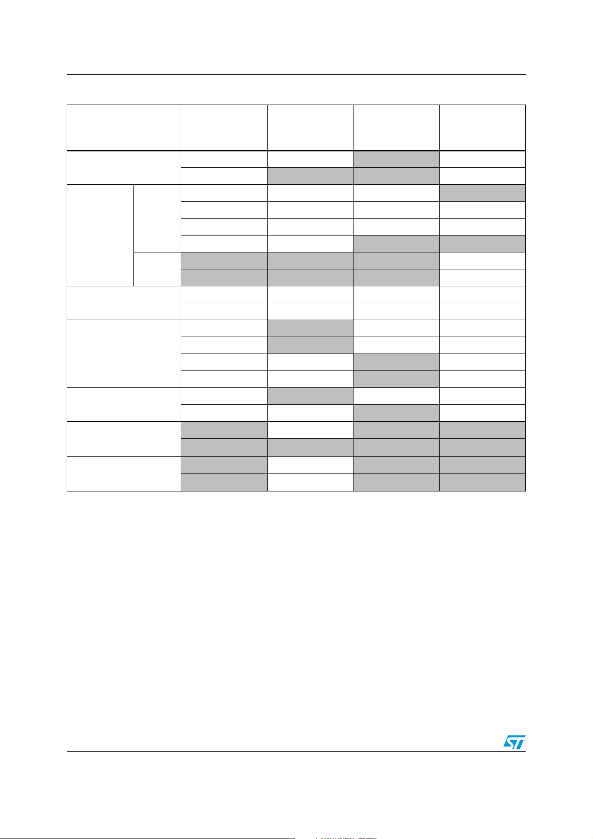
Table 3. Advanced timer configurations
Control bits Output state
Typical use
General purpose
Motor control
(sinewave)
MOE OSSI OSSR OCxE OCxNE
x 0 0 0 Output disable Output disable
x 0 0 1 Output disable
x010
x011
OCx output
state
OCxREF
+ Polarity
OCxREF
+ Polarity
+ Deadtime
OCxN output
state
OCxREF
+ Polarity
Output disable
(not OCxREF)
+ Polarity
+ Deadtime
1
x 1 0 0 Output disabled Output disabled
x 1 0 1 Off-state
x110
x111
MOE OSSI OSSR OCxE OCxNE
0x00
0x01
0x10
0x11
0
1x00
1x01
1x10
1x11
OCxREF
+ Polarity
OCxREF +
Polarity
OCxREF
+ Polarity
+ Deadtime
OCx output
state
Output disable
Off-state
(outputs are first forced with their
inactive level then forced to their
idle level after the deadtime.)
Off-state
(not OCxREF)
+ Polarity
+ Deadtime
OCxN output
state
Motor control
(6-steps)
Motor control
(sinewave)
Comments
Outputs
disconnected
from I/O ports
All PWMs OFF
(low Z for safe
stop)
Note: 1 Dead time insertion is enabled by setting both CCxE and CCxNE bits, and the MOE bit.
2 When only OCxN is enabled (CCxE=0, CCxNE=1), it is not complemented and becomes
active as soon as OCxREF is high. For example, if CCxNP=0 then OCxN=OCxRef. On the
other hand, when both OCx and OCxN are enabled (CCxE=CCxNE=1) OCx becomes
active when OCxREF is high, whereas OCxN is complemented and becomes active when
OCxREF is low.
Doc ID 022500 Rev 1 17/27
Page 18
Advanced features for motor control AN4013
MS30125V2
OC1REF
CH1
CH1N
Delay
Delay
5.2 Specific features for motor control applications
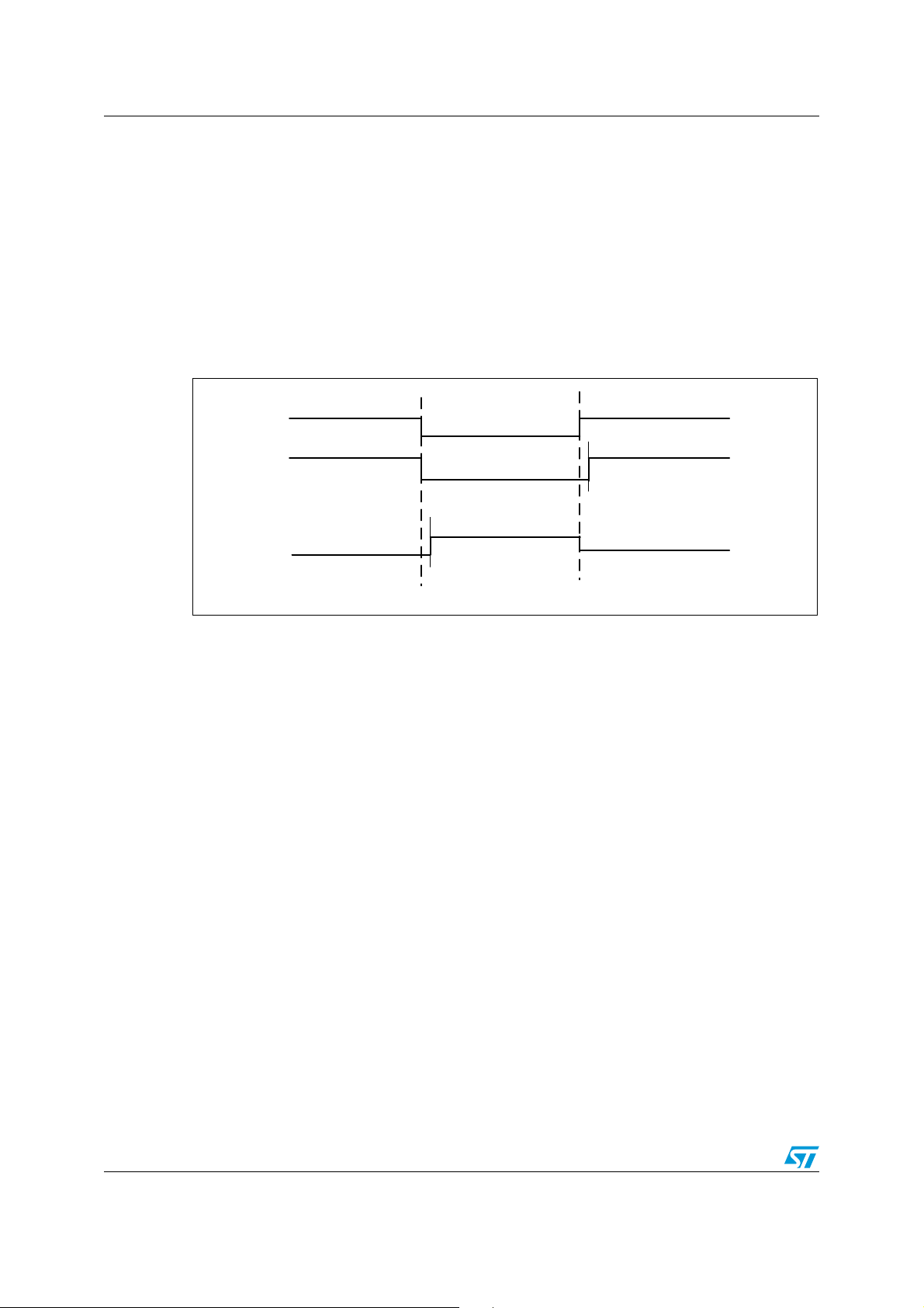
5.2.1 Complementary signal and dead time feature
STM32 advanced timers can generate up to three complementary outputs with insertion of
dead time.
To use the complementary signal for one channel, set the two output compare enable bits of
this channel and its complementary (OCxE and OCxNE) channel.If the dead time bits are
different from zero, the two signals are generated with insertion of a dead time as illustrated
in Figure 2: Two signals are generated with insertion of a dead time:
Figure 2. Two signals are generated with insertion of a dead time
The dead time parameter is computed using the DTG[7:0] bits and the dead time clock
(Tdtg).
The dead time clock is computed as follows:
Tdtg = TDTS, if DTG[7] = 0
Tdtg = 2 x TDTS, if DTG[6] = 0
Tdtg = 8 x TDTS, if DTG[5] = 0
Tdtg = 16 x TDTS, if DTG[7:5] = 111
Where: TDTS = TCK_INT, if CKD[1:0] = 00
TDTS = 2 x TCK_INT, if CKD[1:0] = 01
TDTS = 4 x TCK_INT, if CKD[1:0] = 10
Note: TCK_INT is the timer internal clock.
18/27 Doc ID 022500 Rev 1
Page 19

AN4013 Advanced features for motor control
The dead time delay is computed using the following formula:
Dead time = DTG[7:0]x Tdtg, if DTG[7] = 0
Dead time = (64+DTG[5:0]) x Tdtg, if DTG[6] = 0
Dead time = (32+DTG[4:0]) x Tdtg, if DTG[5] = 0
Dead time = (32+DTG[4:0]) x Tdtg, if DTG[7:5] = 111
For more details on using the timer in this mode, refer to the examples provided in the
STM32xx standard peripheral libraries, in the /Project/STM32xx_StdPeriph_Examples/
TIM/ComplementarySignals folder.
Note: This example is not available for STM32L1xx devices.
5.2.2 Break input
The break input is an emergency input in the motor control application. The break function
protects power switches driven by PWM signals generated with the advanced timers. The
break input is usually connected to fault outputs of power stages and 3-phase inverters.
When activated, the break circuitry shuts down the TIM outputs and forces them to a
predefined safe state.
The break event is generated by:
● The BRK input that has a programmable polarity and an enable bit BKE.
● The CSS (Clock Security System).
● Software, by setting the BG bit in the EGR register.
When a break event occurs:
● The MOE bit (main output enable) is cleared.
● The break status flag is set and an interrupt request can be generated.
● Each output channel is driven with the level programmed in the OISx bit.
Doc ID 022500 Rev 1 19/27
Page 20

Advanced features for motor control AN4013
5.2.3 Locking mechanism
The advanced timers registers and bits can be protected or locked in order to safeguard the
application using the locking mechanism by programming the LOCK bits in the BDTR
register. There are three locking levels.
Table 4. Locking levels
Level 1 Level 2 Level 3
Register Bits Register Bits Register Bits
CR2
BDTR
OISx
OISxN OISxN OISxN
DTG[7:0]
BKE BKE BKE
BKP BKP BKP
AOE AOE AOE
CR2
BDTR
CCER
OISx
CR2
DTG[7:0]
BDTR
OSSR OSSR
OSSI OSSI
CCxP
CCER
CCxNP CCxNP
CCMRx
OISx
DTG[7:0]
CCxP
OCxM
OCxPE
Note: The LOCK bits can be written only once after the reset. Once the BDTR register has been
written, its content is frozen until the next reset.
5.2.4 Specific features for feedback measurement
Encoder modes
The incremental encoder is a type of sensor used in motor-control applications to measure
the angular position.
In general, the incremental encoder generates three signals: phase A, phase B and index.
The direction of the motor depends if Phase A leads Phase B, or Phase B leads Phase A. A
third channel, Index pulse, occurs once per revolution and is used as a reference to
measure an absolute position.
The Phase A and B output signals are connected to the encoder interface to compute the
frequency and then deduce the velocity and the position. Velocity and position information
can be measured at X2 or X4 resolution. The following figures explain the encoder interface
function.
The timer's counter is incremented or decremented for each transition on both inputs TI1
and TI2.
20/27 Doc ID 022500 Rev 1
Page 21

AN4013 Advanced features for motor control
MS30129V1
forward reversal backward forwardreversal
DownUp Up
0
1
0
TI1
TI2
Counter
DIR bit
+1
+1
+1
+1
+1 +1
+1
+1
+1 +1+1+1
+1 +1
+1
+1
-1 -1 -1 -1 -1 -1 -1 -1
MS30128V1
forward reversal backward forwardreversal
DownUp Up
0
1
0
TI1
TI2
Counter
DIR bit
+1
+1 +1 +1
+1
+1
-1
-1
-1 -1
+1
+1
Figure 3. Position at X4 resolution
The timer's counter is incremented or decremented for each transition on the selected input
TI1 or TI2.
Figure 4. Position at X2 resolution
Note: The counter in case of resolution X2 can also be incremented on the TI1 edge.
In STM32 timer encoder interface mode, the encoder mode3 corresponds to resolution X4.
In this mode, the counter counts up/down on both TI1 and TI2 edges.
The resolution X2 is selected when encoder mode 1 or mode 2 is selected, that is, the
counter counts up/down on TI2 edge depending on the TI1 level, or the counter counts
up/down on TI1 edge depending on TI2 level.
How to use the encoder interface
An external incremental encoder can be connected directly to the MCU without external
interface logic. The third encoder output (index) which indicates the mechanical zero
position, may be connected to an external interrupt input and trigger a counter reset.
The output signal of the incremental encoder is filtered by the STM32 timer input filter block
to reject all noise sources that typically occur in motor systems. This filter is used as
described in Section 3.3: Timer input capture mode.
Doc ID 022500 Rev 1 21/27
Page 22

Advanced features for motor control AN4013
MS30127V1
B
OF
B
RF
Sensor output
TIM configuration in encoder mode
1. Select and configure the timer input:
● Input selection:
– TI1 connected to TI1FP1 CC1S='01' in CCMR1 register
– TI2 connected to TI2FP2 CC2S='01' in CCMR1 register
● Input polarity:
– CC1P='0' and CC1NP='0'(CCER register, TI1FP1 non-inverted, TI1FP1=TI1).
– CC2P='0' and CC2NP='0'(CCER register, TI1FP2 non-inverted, TI1FP2= TI2).
2. Select the encoder mode
● Encoder mode1 (resolution X2 on TI2): SMS=’001’ in SMCR register.
● Encoder mode2 (resolution X2 on TI1): SMS=’010' in SMCR register.
● Encoder mode3 (resolution X4 on TI1 and TI2): SMS=’011’ in SMCR register.
3. Enable the timer counter
● Set the counter enable bit, CEN='1' in CR1 register.
Hall sensor
The Hall sensor is a type of sensor based on Hall effect: when a conductor is placed in a
magnetic field, a voltage will be generated perpendicular to both the current and the
magnetic field.
There are four types of Hall sensor IC devices that provide a digital output: unipolar
switches, bipolar switches, omnipolar switches, and latches. The main difference between
them is the output waveforms (pulse duration).
The digital Hall sensor provides a digital output in relation to the magnetic field to which it is
exposed. When the magnetic field increases and is greater than the BRP (magnetic field
release point value), the output will be ON. When the magnetic field decreases and is lower
than the BOP (magnetic field operate point value) the output will be OFF.
Figure 5 presents the output waveform of a typical Hall sensor.
Figure 5. Output waveform of a typical Hall sensor
Generally, the Hall sensor is used in the 3 phase motor control. Figure 6: Commutation
sequence presents the commutation sequence.
22/27 Doc ID 022500 Rev 1
Page 23

AN4013 Advanced features for motor control
MS30126V1
Motor position
Hall 1
Hall 3
Hall 2
0 60 120 180 240 300 360 420 480 540 600 660
Figure 6. Commutation sequence
How to use the Hall sensor interface
The STM32 timers can interfaces with the Hall effect sensors via the standard inputs (CH1,
CH2 and CH3). Setting TI1S bit in the CR2 register, allows the input filter of channel 1 to be
connected to the output of a XOR gate, combining the three input pins TIMx_CH1,
TIMx_CH2 and TIMx_CH3.
The slave mode controller is configured in reset mode; the slave input is TI1F_ED. Thus,
each time one of the 3 inputs toggles, the counter restarts counting from 0. This creates a
time base triggered by any change on the Hall inputs.
Channel 1 is configured in input capture mode, capture signal is TRC. The captured value,
which corresponds to the time, elapsed between 2 changes on the inputs, gives information
about motor speed.
TIM configuration in Hall sensor interface mode
1. Configure 3 timer inputs ORed to the TI1 input channel by writing the TI1S bit in CR2
register to '1',
2. Program the time base: write the ARR to the max value (the counter must cleared by
the TI1 change. Set the prescaler to get a maximum counter period longer than the
time between 2 changes on the sensors,
3. Program channel 1 in capture mode (TRC selected): write the CC1S bits in the CCMR1
register to '01'. You can also program the digital filter if needed.
Doc ID 022500 Rev 1 23/27
Page 24

Specific applications AN4013
6 Specific applications
6.1 Infrared application
The STM32 general purpose timers can be use to emulate several infrared protocol. An
example of this application is explained in application note AN3174 “Implementing an RC5
infrared remote control receiver with the STM32F10xx microcontrollers”.
This application note describes a software solution for implementing an RC5 receiver using
the STM32 general purpose timers.
6.2 3-phase AC and PMSM control motor
The STM32 advanced and general purpose timers with ADC and DAC are used to control
two types of 3-phase motor: AC induction motor and PMSM, with different current sensing
methodologies:
● Isolated current sensing
● Three shunt resistors
● Single shunt resistor (ST patented solution)
The STM32 timers are used also in the feedback loop to interface with the different sensors
used in the different rotor position feedback:
● Tacho generator
● Quadrature encoder
● Hall sensors: 60° and 120° placement
For more details, please refer to: stm32_pmsm_foc_motorcontrol_fmlib.
6.3 Six-step mode
The six step mode is a specific mode of STM32 advanced timers. When complementary
outputs are used on a channel, preload bits are available on the OCxM, CCxE and CCxNE
bits. The preload bits are transferred to the shadow bits at the COM (commutation event).
Thus you can program in advance the configuration for the next step and change the
configuration of all the channels at the same time. COM can be generated by software by
setting the COM bit in the EGR register or by hardware (on TRGI rising edge).
An application example of the use of this mode is the control of the stepper motor.
24/27 Doc ID 022500 Rev 1
Page 25

AN4013 Specific applications
Configuring the timer to generate a six step signal to control a stepper motor:
● Time base configuration: prescaler, period, clock source
● Channels 1, 2, 3 and 4 configured in PWM mode
● Set the capture compare preload control bit CCPC
● Enable the commutation interrupt source
● Use the systemtick to generate time base
● Each commutation event, the TIM configuration is updated for the next commutation
event.
For more details on using the timer in this mode, refer to the examples provided in the
STM32xx standard peripheral libraries, in the /Project/STM32xx_StdPeriph_Examples/
TIM/6Steps folder.
Note: This example is not available for STM32L1xx devices.
Doc ID 022500 Rev 1 25/27
Page 26

Revision history AN4013
7 Revision history
Table 5. Document revision history
Date Revision Changes
21-Feb-2012 1 Initial release.
26/27 Doc ID 022500 Rev 1
Page 27

AN4013
Please Read Carefully:
Information in this document is provided solely in connection with ST products. STMicroelectronics NV and its subsidiaries (“ST”) reserve the
right to make changes, corrections, modifications or improvements, to this document, and the products and services described herein at any
time, without notice.
All ST products are sold pursuant to ST’s terms and conditions of sale.
Purchasers are solely responsible for the choice, selection and use of the ST products and services described herein, and ST assumes no
liability whatsoever relating to the choice, selection or use of the ST products and services described herein.
No license, express or implied, by estoppel or otherwise, to any intellectual property rights is granted under this document. If any part of this
document refers to any third party products or services it shall not be deemed a license grant by ST for the use of such third party products
or services, or any intellectual property contained therein or considered as a warranty covering the use in any manner whatsoever of such
third party products or services or any intellectual property contained therein.
UNLESS OTHERWISE SET FORTH IN ST’S TERMS AND CONDITIONS OF SALE ST DISCLAIMS ANY EXPRESS OR IMPLIED
WARRANTY WITH RESPECT TO THE USE AND/OR SALE OF ST PRODUCTS INCLUDING WITHOUT LIMITATION IMPLIED
WARRANTIES OF MERCHANTABILITY, FITNESS FOR A PARTICULAR PURPOSE (AND THEIR EQUIVALENTS UNDER THE LAWS
OF ANY JURISDICTION), OR INFRINGEMENT OF ANY PATENT, COPYRIGHT OR OTHER INTELLECTUAL PROPERTY RIGHT.
UNLESS EXPRESSLY APPROVED IN WRITING BY TWO AUTHORIZED ST REPRESENTATIVES, ST PRODUCTS ARE NOT
RECOMMENDED, AUTHORIZED OR WARRANTED FOR USE IN MILITARY, AIR CRAFT, SPACE, LIFE SAVING, OR LIFE SUSTAINING
APPLICATIONS, NOR IN PRODUCTS OR SYSTEMS WHERE FAILURE OR MALFUNCTION MAY RESULT IN PERSONAL INJURY,
DEATH, OR SEVERE PROPERTY OR ENVIRONMENTAL DAMAGE. ST PRODUCTS WHICH ARE NOT SPECIFIED AS "AUTOMOTIVE
GRADE" MAY ONLY BE USED IN AUTOMOTIVE APPLICATIONS AT USER’S OWN RISK.
Resale of ST products with provisions different from the statements and/or technical features set forth in this document shall immediately void
any warranty granted by ST for the ST product or service described herein and shall not create or extend in any manner whatsoever, any
liability of ST.
ST and the ST logo are trademarks or registered trademarks of ST in various countries.
Information in this document supersedes and replaces all information previously supplied.
The ST logo is a registered trademark of STMicroelectronics. All other names are the property of their respective owners.
© 2012 STMicroelectronics - All rights reserved
STMicroelectronics group of companies
Australia - Belgium - Brazil - Canada - China - Czech Republic - Finland - France - Germany - Hong Kong - India - Israel - Italy - Japan -
Malaysia - Malta - Morocco - Philippines - Singapore - Spain - Sweden - Switzerland - United Kingdom - United States of America
www.st.com
Doc ID 022500 Rev 1 27/27
 Loading...