How it Works
Log In / Sign Up
Buy Points
How it Works
FAQ
Contact Us
Questions and Suggestions
Users
Datasheet
Loading...
A
AN3310
AN3311
AN3316
AN3316K
AN3317
AN3319
AN3320
AN3321
AN3324
AN3327
AN3328S
AN3329
AN3332
AN3334
AN3336SB
AN3339
AN3340
AN3341SC
AN3342
AN3352
AN3353
AN3354
AN3355
AN3357
AN3358
AN3358SH
AN3359
AN3360
AN3361
AN3362
AN3364
AN3365
AN3370K
AN3371
AN3371SB
AN3375S
AN3383
AN3389SB
AN3390
AN3392
AN3393
AN3394
AN3395
AN3398
AN3399
AN3400
AN3404
AN3406
AN3407
AN3408
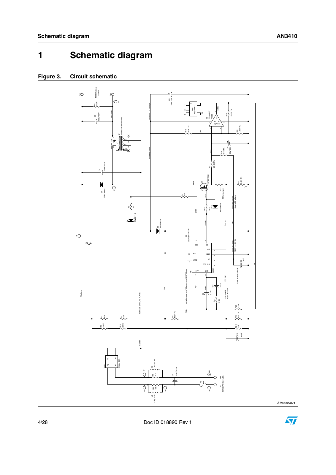
AN3410
AN3411
AN3413
AN3422
AN3424
AN3427
AN3429
AN3430
AN3433
AN3479FBP
AN349
AN3497SB
AN3501NFBP
AN351
AN352
AN354
AN355
AN3592K
AN3592S
AN360
2
AN361
AN362
AN364
AN366
AN3664NFB
AN3672NFBP
AN368
AN369
AN381
AN3811NK
AN3821K
AN3824K
AN3861SA
AN3895FHQ
AN392
2
AN394
2
AN3954
AN3955
AN3959
AN3960
AN3961
AN3964
AN3966
AN3967
AN3968
AN3969
AN3969K
AN3970
AN3972
AN3973
Loading...
Loading...
Nothing found
AN3410
APPLICATION NOTE (ST)
28 pgs
2 Mb
0
Table of contents
Loading...
Datasheet AN3410 APPLICATION NOTE (ST)
...
Datasheet APPLICATION NOTE (ST)
Download
Specifications and Main Features
Frequently Asked Questions
User Manual
Download
Page 1
Page 2
Page 3
Page 4
Page 5
Page 6
Page 7
Page 8
Page 9
Page 10
Page 11
Page 12
Page 13
Page 14
Page 15
Page 16
Page 17
Page 18
Page 19
Page 20
Page 21
Page 22
Page 23
Page 24
Page 25
Page 26
Page 27
Page 28
Loading...
+
hidden pages
Unhide
You need points to download manuals.
1 point = 1 manual.
You can buy points or you can get point for every manual you upload.
Buy points
Upload your manuals


")