

Page 1
AN3395
Application note
Sensing resistor selection and usage
in STC310x battery monitoring applications
Introduction
Voltage measurement and coulomb counting are the two most common methods used to
implement battery monitoring for gas gauge applications. Although the use of voltage
measurement has been a popular method, it does not produce the most accurate results.
The STC310x series battery monitor ICs developed by STMicroelectronics combine the two
methods into one integrated solution. It updates the battery State-of-Charge (SOC) at light
load (relaxation/standby period) with the real battery Open-Circuit-Voltage (OCV) while
using coulomb counting to track the battery capacity under heavy load to provide the most
accurate SOC value under all application conditions.
In coulomb counting, the sensing resistor is used to measure the battery current. The
specified maximum voltage drop on the sensing resistor is only 80 mV, thus it plays an
important role in the gas gauge accuracy and merits careful attention. This document
describes:
■ the sensing resistor (Rcg) selection
■ the Rcg power considerations
■ the Rcg layout recommendations
December 2011 Doc ID 018779 Rev 1 1/11
www.st.com
Page 2

Contents AN3395
Contents
1 STC310x external components . . . . . . . . . . . . . . . . . . . . . . . . . . . . . . . . 3
2 Rcg resistance selection . . . . . . . . . . . . . . . . . . . . . . . . . . . . . . . . . . . . . 4
2.1 Maximum peak current in the application . . . . . . . . . . . . . . . . . . . . . . . . . . 4
2.2 Power rating of the resistor . . . . . . . . . . . . . . . . . . . . . . . . . . . . . . . . . . . . . 4
2.3 ADC code usage efficiency . . . . . . . . . . . . . . . . . . . . . . . . . . . . . . . . . . . . 4
2.4 Selection of Rcg (example) . . . . . . . . . . . . . . . . . . . . . . . . . . . . . . . . . . . . 5
3 Rcg power loss consideration . . . . . . . . . . . . . . . . . . . . . . . . . . . . . . . . . 6
4 Rcg layout considerations . . . . . . . . . . . . . . . . . . . . . . . . . . . . . . . . . . . . 7
5 Conclusion . . . . . . . . . . . . . . . . . . . . . . . . . . . . . . . . . . . . . . . . . . . . . . . . . 9
6 Revision history . . . . . . . . . . . . . . . . . . . . . . . . . . . . . . . . . . . . . . . . . . . 10
2/11 Doc ID 018779 Rev 1
Page 3
AN3395 STC310x external components
1 STC310x external components
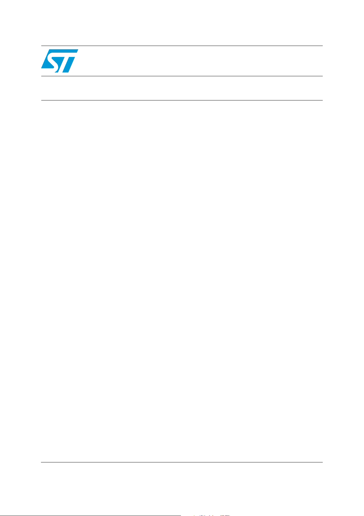
Figure 1 illustrates the typical connections for a gas gauge application using the STC3105.
The SDA, SCL and ALM (I/O0 in the STC3100) pins are open drain and require external
pull-up resistors to either system I/O voltage or V
components shown in Figure 1 connected to the V
additional ESD protection and input filtering, please refer to AN3064 for more information.
The resistor (Rcg) connected between the CG and GND pins is the sensing resistor. In
order to obtain higher accuracy, refer to the following application guidelines.
Figure 1. STC3105 typical connections
System I/O supply
Rpu1
Rpu2
Rpu3
STC3105
ALM
(pull up to battery voltage). The
CC
and VIN pins are used to provide
CC
System supply
VCC
C1C2D1
R1
MCU
SDA
SCL
GND
VIN
CG
R2
Battery
R
cg
Gnd
AM045291v1
Doc ID 018779 Rev 1 3/11
Page 4

Rcg resistance selection AN3395
2 Rcg resistance selection
The Rcg resistor is used to sense the current flowing "into" or "out of" the battery. The
voltage drop on Rcg is input to the current measurement ADC through the CG pin. There
are three common rules for the selection of the Rcg resistance:
1. Maximum peak current
2. Power rating
3. ADC code usage
2.1 Maximum peak current in the application
As specified in the datasheet (refer to the STC3105 or STC3100 datasheet), the voltage
drop across the Rcg resistor (input voltage range on CG pin) must not exceed ±80 mV. That
is Rcg x I
Equation 1.
Equation 1
must be ≤ 80 mV. This gives a maximum limit for the Rcg resistor value in
PEAK
80 mv()
Rcg mΩ()
-----------------------
≤
I
PEAK
A()
2.2 Power rating of the resistor
The second step is to consider the power dissipation limit of the resistor as given in Equation
2. The power dissipation in the resistor must be kept within the power rating of the resistor
calculated by:
Equation 2
Power dissipation = Rcg x I
Note: Must be less than the power rating of the resistor
However, it may be better to choose a smaller resistance value with a smaller power rating
to:
● have a smaller PCB footprint and
● reduce the power loss in the resistor.
RMS
2
2.3 ADC code usage efficiency
The full scale voltage range of the ADC is designed for the input on the CG pin to reach
±80 mV (max). To make better use of the ADC performance, Rcg must not be too small:
Rcg x I
must be > 40 mV for a reasonable ADC code usage.
PEAK
4/11 Doc ID 018779 Rev 1
Page 5

AN3395 Rcg resistance selection
2.4 Selection of Rcg (example)
Assume I
= 2.2 A and I
PEAK
= 1.5 A in a mobile phone.
RMS
According to Equation 1, the maximum limit of Rcg is obtained, that is Rcg < 36 mΩ.
Let's choose a 33 mΩ resistor.
Power rating = 33 mΩ x 1.5
2
A = 74 mW
Therefore, a 1/8 W (125 mW) resistor is sufficient, however, it is possible to use a 20 mΩ
resistor that will only dissipate 45 mW instead of 74 mW.
A 20 mΩ resistor is optimal because 20 mΩ x 2.2 A = 44 mV, which is acceptable in
comparison with the full scale range of 80 mV.
Doc ID 018779 Rev 1 5/11
Page 6

Rcg power loss consideration AN3395
3 Rcg power loss consideration
The power loss of the Rcg should be considered. Let's look at the worst case when the
mobile phone is drawing current during continuous talk time.
Assuming a battery with capacity of 5.55 Wh (1500 mAh) and a 300 mA average current
consumption (5 hours talk time), and assuming typical GSM load current waveform below in
Figure 2:
Figure 2. Typical GSM load profile
~2 A
~4.1 ms
Avg
Current (mA)
0.5 ms
~70 mA
Time (ms)
AM045292v1
For the power loss calculation we must consider RMS current, not average current:
Equation 3
I
RMS
220.5 0.07
------------------------------------------------------- - 0.66A==
2
+× 4.1×
4.6
Equation 4
Power loss = Rcg x I
2
x talk time = 0.02 x 0.662 x 5 = 0.044 Wh
RMS
0.044 Wh equals 0.8% of battery capacity (5.55 Wh).
This is the worst case condition. If the device is not used in continuous talking mode but in
mixed mode usage (with lower RMS power consumption), the power loss will be less and
will not significantly affect the accuracy of the battery capacity measurement.
6/11 Doc ID 018779 Rev 1
Page 7

AN3395 Rcg layout considerations
4 Rcg layout considerations
Figure 3 shows the recommended layout of the PCB for Rcg.
Figure 3. Rcg recommended layout with the STC3105
AM045293v1
In order to obtain the most accurate SOC estimation, follow these recommendations:
1. Place Rcg as close as possible to the CG pin.
The STC3105 measures the battery current by sensing the voltage between the CG
and GND pin. Between these two pins are two PCB traces and Rcg. Any voltage drop
on the traces will directly add error to the measurement. The shorter the traces are, the
better the accuracy of the measurement obtained.
2. The STC3105 GND pin should be connected directly to a terminal of Rcg (CG– in
Figure 3), not through the ground plane. This Rcg terminal (CG– in Figure 3) should
be connected to the ground plane on the PCB.
This connection avoids the occurrence of high current through Rcg to the voltage
potential on the STC3105 GND pin. Any ground disturbances will directly affect the
accuracy of the current measurement and therefore the SOC estimation.
3. If the STC3105 is on a PCB near RF components, special care should be taken to
avoid ground disturbance by the RF interference.
The user can simply connect two high-frequency ceramic capacitors in parallel with
Rcg
to minimize the RF effect, if needed. The capacitance should be selected based on
the frequencies which produce the highest RF disturbance. For example,
15 pF (ex. Murata 15 pF, part code: GQM2195C2A150GB01) and 68 pF (ex. Murata
68 pF, part code: GQM1885C1H680GB01) can be selected to avoid the disturbances
from 1.8 GHz and 900 MHz (strongest RF power in a cell phone). This is illustrated in
Figure 4 on page 8.
Doc ID 018779 Rev 1 7/11
Page 8

Rcg layout considerations AN3395
Figure 4. Capacitive filtering using ceramic capacitors
Main PCB
Battery
Battery connectors
Sensing resistor
Capacitors
STC3105
RF source
AM045294v1
8/11 Doc ID 018779 Rev 1
Page 9

AN3395 Conclusion
5 Conclusion
This document provides guidance to the user for the selection, the power consumption
consideration and the layout of the sensing resistor used with the STC310x battery monitor
for gas gauge applications. In most applications, 33 mΩ or 20 mΩ resistance is preferred to
avoid power consumption concerns. With regards to PCB layout, the sensing resistor should
be positioned as close to the STC310x as possible and the two terminals of Rcg directly
connected to the CG and GND pins of the STC310x. The sensing resistor should be
connected to the PCB ground plane. In the event of RF frequency exposure, capacitive
filtering should be implemented by the parallel placement of high-frequency ceramic
capacitors to avoid the disturbance of the GND pin of the STC310x for more accurate SOC
measurement.
Doc ID 018779 Rev 1 9/11
Page 10

Revision history AN3395
6 Revision history
Table 1. Document revision history
Date Revision Changes
05-Dec-2011 1 Initial release.
10/11 Doc ID 018779 Rev 1
Page 11

AN3395
Please Read Carefully:
Information in this document is provided solely in connection with ST products. STMicroelectronics NV and its subsidiaries (“ST”) reserve the
right to make changes, corrections, modifications or improvements, to this document, and the products and services described herein at any
time, without notice.
All ST products are sold pursuant to ST’s terms and conditions of sale.
Purchasers are solely responsible for the choice, selection and use of the ST products and services described herein, and ST assumes no
liability whatsoever relating to the choice, selection or use of the ST products and services described herein.
No license, express or implied, by estoppel or otherwise, to any intellectual property rights is granted under this document. If any part of this
document refers to any third party products or services it shall not be deemed a license grant by ST for the use of such third party products
or services, or any intellectual property contained therein or considered as a warranty covering the use in any manner whatsoever of such
third party products or services or any intellectual property contained therein.
UNLESS OTHERWISE SET FORTH IN ST’S TERMS AND CONDITIONS OF SALE ST DISCLAIMS ANY EXPRESS OR IMPLIED
WARRANTY WITH RESPECT TO THE USE AND/OR SALE OF ST PRODUCTS INCLUDING WITHOUT LIMITATION IMPLIED
WARRANTIES OF MERCHANTABILITY, FITNESS FOR A PARTICULAR PURPOSE (AND THEIR EQUIVALENTS UNDER THE LAWS
OF ANY JURISDICTION), OR INFRINGEMENT OF ANY PATENT, COPYRIGHT OR OTHER INTELLECTUAL PROPERTY RIGHT.
UNLESS EXPRESSLY APPROVED IN WRITING BY TWO AUTHORIZED ST REPRESENTATIVES, ST PRODUCTS ARE NOT
RECOMMENDED, AUTHORIZED OR WARRANTED FOR USE IN MILITARY, AIR CRAFT, SPACE, LIFE SAVING, OR LIFE SUSTAINING
APPLICATIONS, NOR IN PRODUCTS OR SYSTEMS WHERE FAILURE OR MALFUNCTION MAY RESULT IN PERSONAL INJURY,
DEATH, OR SEVERE PROPERTY OR ENVIRONMENTAL DAMAGE. ST PRODUCTS WHICH ARE NOT SPECIFIED AS "AUTOMOTIVE
GRADE" MAY ONLY BE USED IN AUTOMOTIVE APPLICATIONS AT USER’S OWN RISK.
Resale of ST products with provisions different from the statements and/or technical features set forth in this document shall immediately void
any warranty granted by ST for the ST product or service described herein and shall not create or extend in any manner whatsoever, any
liability of ST.
ST and the ST logo are trademarks or registered trademarks of ST in various countries.
Information in this document supersedes and replaces all information previously supplied.
The ST logo is a registered trademark of STMicroelectronics. All other names are the property of their respective owners.
© 2011 STMicroelectronics - All rights reserved
STMicroelectronics group of companies
Australia - Belgium - Brazil - Canada - China - Czech Republic - Finland - France - Germany - Hong Kong - India - Israel - Italy - Japan -
Malaysia - Malta - Morocco - Philippines - Singapore - Spain - Sweden - Switzerland - United Kingdom - United States of America
www.st.com
Doc ID 018779 Rev 1 11/11
 Loading...