

Page 1
STA350BW 2.0-channel demonstration board
)
Introduction
The purpose of this application note is to describe:
■ how to connect the STA350BW 2.0-channel demonstration board
■ how to evaluate the demonstration board performance with all the electrical curves
■ how to avoid critical issues in the PCB schematic and layout of the the STA350BW
The STA350BW demonstration board is specifically configured for 2.0 BTL channels,
releasing up to 2 x 50 W into 6 ohm of power output at 25 V of supply voltage using reduced
components. It is a complete solution for the digital audio power amplifier.
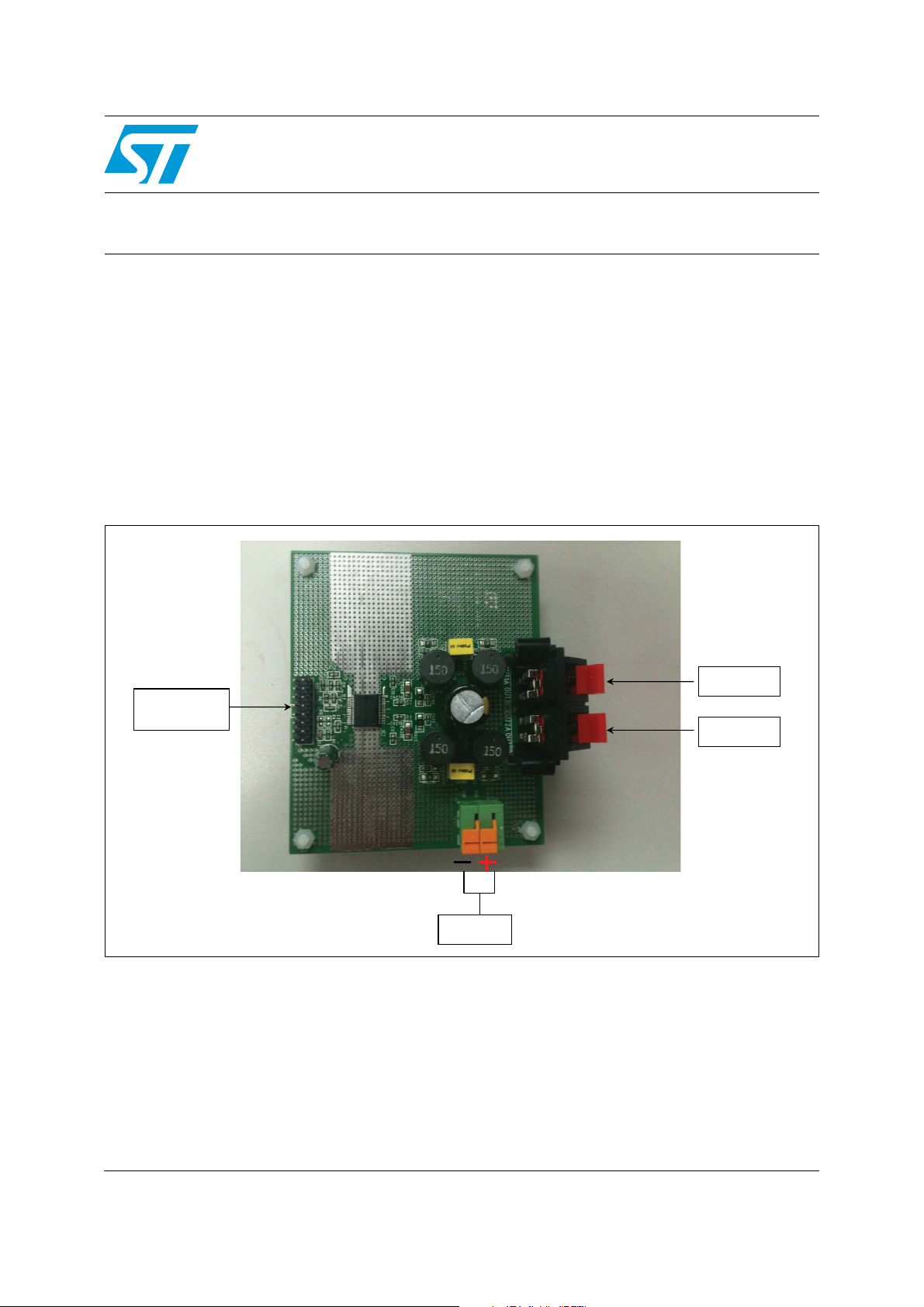
Figure 1. STA350BW 2.0-channel demonstration board
AN3383
Application note
Connected with AP
WLink boa rd (I2C
& I2S
VCC
DC 4.5-26V
Speaker Output
L CH
Speaker Output
R CH
AM045230v1
April 2011 Doc ID 018691 Rev 1 1/29
www.st.com
Page 2

Contents AN3383
Contents
1 Functional description of the demonstration board . . . . . . . . . . . . . . . 4
1.1 Connections . . . . . . . . . . . . . . . . . . . . . . . . . . . . . . . . . . . . . . . . . . . . . . . . 4
1.2 Output configuration . . . . . . . . . . . . . . . . . . . . . . . . . . . . . . . . . . . . . . . . . . 4
1.3 Schematic and block diagrams, PCB layout, bill of material . . . . . . . . . . . . 5
2 Test results . . . . . . . . . . . . . . . . . . . . . . . . . . . . . . . . . . . . . . . . . . . . . . . . 9
3 Thermal test results . . . . . . . . . . . . . . . . . . . . . . . . . . . . . . . . . . . . . . . . 14
4 Design guidelines for schematic and PCB layout . . . . . . . . . . . . . . . . 16
4.1 Schematic . . . . . . . . . . . . . . . . . . . . . . . . . . . . . . . . . . . . . . . . . . . . . . . . . 16
4.1.1 Main driver for selection of components . . . . . . . . . . . . . . . . . . . . . . . . 16
4.1.2 Decoupling capacitors . . . . . . . . . . . . . . . . . . . . . . . . . . . . . . . . . . . . . . 16
4.1.3 Output filter . . . . . . . . . . . . . . . . . . . . . . . . . . . . . . . . . . . . . . . . . . . . . . 16
4.2 PCB layout . . . . . . . . . . . . . . . . . . . . . . . . . . . . . . . . . . . . . . . . . . . . . . . . 19
5 Revision history . . . . . . . . . . . . . . . . . . . . . . . . . . . . . . . . . . . . . . . . . . . 28
2/29 Doc ID 018691 Rev 1
Page 3

AN3383 List of figures
List of figures
Figure 1. STA350BW 2.0-channel demonstration board . . . . . . . . . . . . . . . . . . . . . . . . . . . . . . . . . . . 1
Figure 2. Schematic diagram . . . . . . . . . . . . . . . . . . . . . . . . . . . . . . . . . . . . . . . . . . . . . . . . . . . . . . . . 5
Figure 3. Block diagram of test connections with equipment . . . . . . . . . . . . . . . . . . . . . . . . . . . . . . . . 6
Figure 4. Top view of PCB layout . . . . . . . . . . . . . . . . . . . . . . . . . . . . . . . . . . . . . . . . . . . . . . . . . . . . 7
Figure 5. Bottom view of PCB layout . . . . . . . . . . . . . . . . . . . . . . . . . . . . . . . . . . . . . . . . . . . . . . . . . . 7
Figure 6. Efficiency (2 channels, BTL configuration), V
Figure 7. Efficiency (2 channels, BTL configuration), V
Figure 8. Output power vs. supply voltage, R
Figure 9. Output power vs. supply voltage, R
Figure 10. Frequency response, V
Figure 11. Crosstalk, V
Figure 12. SNR, V
CC
= 24 V, RL = 6 ohm, 0 dB (Pout = 1 W) . . . . . . . . . . . . . . . . . . . . . . . . . . . 12
CC
= 24 V, RL = 6 ohm, 0 dB (Pout = 1 W) . . . . . . . . . . . . . . . . . . . . . . . . . . . . . . . 12
Figure 13. THD vs. frequency, V
Figure 14. FFT (0 dBFS), V
Figure 15. FFT (-60 dBFS), V
= 24 V, RL = 6 ohm, 0 dBFS (Pout = 1 W) . . . . . . . . . . . . . . . . . . . . . 13
CC
CC
Figure 16. THD vs. output power, V
Figure 17. Output power = 2 x 5 W, V
Figure 18. Output power = 2 x 10 W, V
Figure 19. Output power = 2 x 15 W, V
Figure 20. Output power = 2 x 38 W, V
= 24 V, RL = 6 ohm, 0 dB (Pout = 1 W) . . . . . . . . . . . . . . . . . . 11
CC
= 24 V, RL = 6 ohm, Pout = 1 W . . . . . . . . . . . . . . . . . . . . . . . . . 12
CC
= 24 V, RL = 6 ohm, 0 dBFS (Pout = 1 W) . . . . . . . . . . . . . . . . . . . . 13
= 24 V, RL = 6 ohm, f = 1 kHz . . . . . . . . . . . . . . . . . . . . . . . . 13
CC
CC
CC
CC
CC
= 6 ohm . . . . . . . . . . . . . . . . . . . . . . . . . . . . . . . . . . 10
L
= 8 ohm . . . . . . . . . . . . . . . . . . . . . . . . . . . . . . . . . . 11
L
= 26 V, load = 6 ohm, frequency = 1 kHz . . . . . . . . . . . . . . 14
= 26 V, load = 6 ohm, frequency = 1 kHz . . . . . . . . . . . . . 14
= 26 V, load = 6 ohm, frequency = 1 kHz . . . . . . . . . . . . . 15
= 26 V, load = 8 ohm, frequency = 1 kHz . . . . . . . . . . . . . 15
Figure 21. Output filter . . . . . . . . . . . . . . . . . . . . . . . . . . . . . . . . . . . . . . . . . . . . . . . . . . . . . . . . . . . . . 16
Figure 22. Power dissipated over the series resistance [P = C*f*(2*V)
Figure 23. Power dissipated over the series resistance [P = C*f*2(V
Figure 24. Damping network . . . . . . . . . . . . . . . . . . . . . . . . . . . . . . . . . . . . . . . . . . . . . . . . . . . . . . . . 18
Figure 25. Main filter . . . . . . . . . . . . . . . . . . . . . . . . . . . . . . . . . . . . . . . . . . . . . . . . . . . . . . . . . . . . . . 18
Figure 26. Recommended power-up and power-down sequence . . . . . . . . . . . . . . . . . . . . . . . . . . . . 19
Figure 27. Snubber network soldered as close as possible to the related IC pin . . . . . . . . . . . . . . . . 19
Figure 28. Electrolytic capacitor used first to separate the V
Figure 29. Path between V
and ground pin minimized in order to avoid inductive paths . . . . . . . . 20
CC
Figure 30. Large ground planes on the top and bottom sides of the PCB . . . . . . . . . . . . . . . . . . . . . . 21
Figure 31. PLL filter soldered as close as possible to the FILT pin . . . . . . . . . . . . . . . . . . . . . . . . . . . 22
Figure 32. Symmetrical paths created for output stage (for differential applications) . . . . . . . . . . . . . 22
Figure 33. Coils separated in order to avoid crosstalk . . . . . . . . . . . . . . . . . . . . . . . . . . . . . . . . . . . . . 22
Figure 34. V
filter for high frequency . . . . . . . . . . . . . . . . . . . . . . . . . . . . . . . . . . . . . . . . . . . . . . . . 23
CC
Figure 35. Decoupling capacitors . . . . . . . . . . . . . . . . . . . . . . . . . . . . . . . . . . . . . . . . . . . . . . . . . . . . 23
Figure 36. Snubber filter for spike high frequency in PWM . . . . . . . . . . . . . . . . . . . . . . . . . . . . . . . . . 24
Figure 37. Correct common-mode and differential snubber placement . . . . . . . . . . . . . . . . . . . . . . . . 24
Figure 38. Correct output routing . . . . . . . . . . . . . . . . . . . . . . . . . . . . . . . . . . . . . . . . . . . . . . . . . . . . . 25
Figure 39. Comparison of output routing . . . . . . . . . . . . . . . . . . . . . . . . . . . . . . . . . . . . . . . . . . . . . . . 25
Figure 40. Thermal layout with large ground (1/3 for top and bottom layers) . . . . . . . . . . . . . . . . . . . 26
Figure 41. Thermal layout with large ground (2/3 for thermal and soldering holes). . . . . . . . . . . . . . . 26
Figure 42. Comparison of thermal layout (top layer) . . . . . . . . . . . . . . . . . . . . . . . . . . . . . . . . . . . . . . 27
Figure 43. Comparison of thermal layout (bottom layer) . . . . . . . . . . . . . . . . . . . . . . . . . . . . . . . . . . . 27
= 26 V, RL = 6 ohm . . . . . . . . . . . . . . . . . . 9
CC
= 26 V, RL = 8 ohm . . . . . . . . . . . . . . . . . 10
CC
2
]. . . . . . . . . . . . . . . . . . . . . . . 17
2
)] . . . . . . . . . . . . . . . . . . . . . . . 17
branches . . . . . . . . . . . . . . . . . . . . . . 20
CC
Doc ID 018691 Rev 1 3/29
Page 4

Functional description of the demonstration board AN3383
1 Functional description of the demonstration board
The following terms used in this application note are defined as follows:
● THD+N vs. Freq: Total harmonic distortion plus noise versus frequency curve
● THD+N vs. Pout: Total Harmonic Distortion (THD) plus noise versus output power
● S/N ratio: Signal-to-noise ratio
● FFT: Fast Fourier Transform Algorithm (method)
● CT: Channel separation L to R, or R to L channel crosstalk
The equipment used includes the following:
● Audio Precision (System 2700) by AP Co., USA)
● DC power supply (4.5 V to 26 V)
● Digital oscilloscope (TDS3034B by Tektronix)
● PC (with APWorkbench GUI control software installed)
1.1 Connections
Power supply signal and interface connection
1. Connect the positive voltage of 24V DC power supply to the +Vcc pin and negative to
GND.
2. Connect the APWorkbench board to the J1 connector of the STA350BW demonstration
board.
3. Connect the S/PDIF signal cable to the RCA jack on the APWLink board, connecting to
the signal source such as Audio precision or DVD player.
Note: The voltage range of the DC power supply for V
1.2 Output configuration
The STA350BW demo board is specifically configured in 2 BTL channels. For the software
setup, please refer to the APWUserManualR1.0.pdf.
is 4.5 V to 26 V.
CC
4/29 Doc ID 018691 Rev 1
Page 5

AN3383 Functional description of the demonstration board
1.3 Schematic and block diagrams, PCB layout, bill of material
Figure 2. Schematic diagram
AM045231v1
Doc ID 018691 Rev 1 5/29
Page 6

Functional description of the demonstration board AN3383
g
(
)
(
)
Figure 3. Block diagram of test connections with equipment
Audio Precision Equipment
Monitor
Output
to AP
S/PDIF
nal
Si
Digital Oscilloscope
TDS3034B Tektronix
STA350BW
Demo B’D
From 4.5V to26V
I2S Input
DC3V3
DC Power Supply
APWLink Board
DC7V
PC with GUI to control the
chipset
AM045232v1
6/29 Doc ID 018691 Rev 1
Page 7

AN3383 Functional description of the demonstration board
Figure 4. Top view of PCB layout
Figure 5. Bottom view of PCB layout
AM045233v1
AM045234v1
Doc ID 018691 Rev 1 7/29
Page 8

Functional description of the demonstration board AN3383
Table 1. Bill of material
No. Type Footprint Description Qty Reference Manufacturer
1 Jack Through-hole 4P Speaker Jack 1 J7 Any source
2 MCAP Through-hole 680NF-M(63V) Capacitor 2 C415SL, C416S Any source
3 Terminal Through-hole 2P Pitch: 5 mm Connector Terminal 1 CN2
4 CNN Through-hole 16P (8 x 2 row) 2.5 mm male CNN 1 J1 Any source
5 CCAP CAP0603 50 volt NPO 330 pF +/- 10% 2 C418A, C425 Murata
6 CCAP CAP0603 50 volt NPO 680 pF +/- 10% 1 C9 Murata
7 CCAP CAP0603 50 volt 1 nF +/- 10% 1 C3 Murata
8 CCAP CAP0603 50 volt 4.7 nF +/- 10% 1 C7 Murata
C2, C4, C5, C11,
C15, C421A,
C421B, C422A,
9 CCAP CAP0603 50 volt 100 nF +/- 10% 15
10 CCAP CAP1206 50 volt 1 µF +/-10% 2 C426A, C426B Murata
11 RES R1206 4R7, +/-5% 1/4W 4
12 RES R1206 20 +/-5% 1/4W 2 R422A, R423 Murata
13 RES R0603 0 ohm 1/16W 1 R31 Murata
C422B, C423A,
C423B, C424A,
C424B, C427A,
C427B
R424A, R424B,
R425A, R425B
Phoenix
Contact
Murata
Murata
14 RES R0603 2R2 +/-5% 1/16W 1 R32 Murata
15 RES R0603 10K +/-5% 1/16W 1 R1 Murata
16 RES R0603 2.2K +/-5% 1/16W 1 R6 Murata
17 RES R0603 NS 2 R4, R5
18 ECAP Through-hole 22 µF/ 16 V 1 C12
19 ECAP Through-hole 1000 µF / 35 V 105 Centigrade 1 C428
20 Plastic rod
21 Plastic rod
22 IC PSSO36 STA350BW 1 IC1 ST
23 Coil Through-hole 15 µH Choke Coil (1014P-01-150L) 4
24 PCB STA350BW 2.0 CH VER1.0 1 Fastprint
Hexagonal rod 15 mm length,
male type
Hexagonal rod 8 mm length,
female type
4 Four Corner
4 Four Corner
L421A, L421B,
L422A, L422B
Rubycon/
Panasonic
Rubycon/
Panasonic
KwangSung
8/29 Doc ID 018691 Rev 1
Page 9

AN3383 Test results
2 Test results
All the results and graphs are from measures using equipment from Audio Precision.
Figure 6. Efficiency (2 channels, BTL configuration), V
+1
+0.9
+0.8
+0.7
+0.6
+0.5
+0.4
+0.3
+0.2
+0.1
+0
5 5510 15 20 25 30 35 40 45 50
W
= 26 V, RL = 6 ohm
CC
AM045235v1
Doc ID 018691 Rev 1 9/29
Page 10

Test results AN3383
Figure 7. Efficiency (2 channels, BTL configuration), VCC = 26 V, RL = 8 ohm
+1
+0.9
+0.8
+0.7
+0.6
+0.5
+0.4
+0.3
+0.2
+0.1
+0
5 4510 15 20 25 30 35 40
W
Figure 8. Output power vs. supply voltage, R
60
55
50
45
40
35
W
30
25
20
15
10
5
= 6 ohm
L
AM045236v1
+6 +26+8 +10 +12 +14 +16 +18 +20 +22 +24
Vdc
10/29 Doc ID 018691 Rev 1
AM045237v1
Page 11

AN3383 Test results
Figure 9. Output power vs. supply voltage, RL = 8 ohm
50
45
40
35
30
W
25
20
15
10
5
+6 +26+8 +10 +12 +14 +16 +18 +20 +22 +24
Vdc
AM045238v1
Figure 10. Frequency response, V
+3
+2
+1
d
B
+0
r
A
-1
-2
-3
20 20k50 100 200 500 1k 2k 5k 10k
= 24 V, RL = 6 ohm, 0 dB (Pout = 1 W)
CC
Hz
AM045239v1
Doc ID 018691 Rev 1 11/29
Page 12

Test results AN3383
Figure 11. Crosstalk, VCC = 24 V, RL = 6 ohm, 0 dB (Pout = 1 W)
+0
-20
-40
d
-60
B
-80
-100
-120
20 20k50 100 200 500 1k 2k 5k 10k
Hz
AM045240v1
Figure 12. SNR, V
+0
-20
d
-40
B
r
-60
A
-80
-100
20 20k50 100 200 500 1k 2k 5k 10k
Figure 13. THD vs. frequency, V
10
5
2
1
0.5
%
0.2
0.1
0.05
= 24 V, RL = 6 ohm, 0 dB (Pout = 1 W)
CC
Hz
= 24 V, RL = 6 ohm, Pout = 1 W
CC
AM045241v1
0.02
0.01
20 20k50 100 200 500 1k 2k 5k 10k
Hz
12/29 Doc ID 018691 Rev 1
AM045242v1
Page 13

AN3383 Test results
Figure 14. FFT (0 dBFS), VCC = 24 V, RL = 6 ohm, 0 dBFS (Pout = 1 W)
+0
-20
-40
d
B
-60
r
-80
A
-100
-120
20 20k50 100 200 500 1k 2k 5k 10k
Hz
AM045243v1
Figure 15. FFT (-60 dBFS), V
+0
-20
-40
d
B
-60
r
-80
A
-100
-120
20 20k50 100 200 500 1k 2k 5k 10k
Figure 16. THD vs. output power, V
10
5
2
1
0.5
%
0.2
0.1
0.05
= 24 V, RL = 6 ohm, 0 dBFS (Pout = 1 W)
CC
Hz
= 24 V, RL = 6 ohm, f = 1 kHz
CC
AM045244v1
0.02
0.01
10m 5020m 50m 100m 200m 500m 1 2 5 10 20
W
Doc ID 018691 Rev 1 13/29
AM045245v1
Page 14

Thermal test results AN3383
3 Thermal test results
Figure 17. Output power = 2 x 5 W, VCC = 26 V, load = 6 ohm, frequency = 1 kHz
Figure 18. Output power = 2 x 10 W, V
= 26 V, load = 6 ohm, frequency = 1 kHz
CC
AM045246v1
14/29 Doc ID 018691 Rev 1
AM045247v1
Page 15

AN3383 Thermal test results
Figure 19. Output power = 2 x 15 W, VCC = 26 V, load = 6 ohm, frequency = 1 kHz
Figure 20. Output power = 2 x 38 W, V
38
37.8
37.6
37.4
37.2
37
36.8
36.6
W
36.4
36.2
36
35.8
35.6
35.4
35.2
35
0 1.8k200 400 600 800 1k 1.2k 1.4k 1.6k
= 26 V, load = 8 ohm, frequency = 1 kHz
CC
sec
AM045248v1
AM045249v1
The device works properly during the entire test time (30 minutes).
Doc ID 018691 Rev 1 15/29
Page 16

Design guidelines for schematic and PCB layout AN3383
4 Design guidelines for schematic and PCB layout
4.1 Schematic
4.1.1 Main driver for selection of components
The characteristics of the main driver are as follows:
● Absolute maximum rating: STA350BW V
● Bypass capacitor 100 nF in parallel to 1 µF for each power V
dielectric is X7R
● Vdd and Ground for PLL filter separated from the other power supply
● Coil saturation current compatible with the peak current of application
4.1.2 Decoupling capacitors
For the decoupling capacitor(s), one decoupling system can be used per channel. The
decoupling capacitor must be as close as possible to the IC pins in order to avoid parasitic
inductance with the copper wire on the PC board.
= 30 V
CC
branch. Preferable
CC
4.1.3 Output filter
Figure 21. Output filter
INxA
INxB
SNUBBER
1. The key function of a snubber network is to absorb energy from the reactance in the
power circuit. The purpose of the snubber RC network is to avoid unnecessary high
pulse energy such as a spike in the power circuit which is dangerous to the system.
L11
C90
330p
R36
20
L13 22u
22u
C89
100n
R34
C95
6.2
100n
C101
100n
C105
100n
R37
6.2
C98
470n
Main Filter Damping Network
C91
1000p
C103
1000p
C99
1000p
J7
1
2
CON2
AM045250v1
16/29 Doc ID 018691 Rev 1
Page 17

AN3383 Design guidelines for schematic and PCB layout
The snubber network allows the energy (big spike) to be transferred to and from the
snubber network in order for the system to be worked on safely.
2. The purpose of the main filter is to limit the frequency higher than the audible range of
20 kHz, which is mandatory in order to have a clean amplifier response. The main filter
is designed using the Butterworth formula to define the cutoff frequency.
3. The purpose of the damping network is to avoid the high-frequency oscillation issue on
the output circuit. The damping network allows the THD to be improved and also allows
avoiding the inductive copper on the PCB route when the system is working on high
frequency with PWM or PCM.
Snubber filter
The snubber circuit must be optimized for the specific application. Starting values are
330 pF in series to 22 ohm. The power on this network is dependent on the power supply,
frequency and capacitor value according to the following formula:
P = C*f*(2*V)
This power is dissipated over the series resistance as shown in Figure 22
2
Figure 22. Power dissipated over the series resistance [P = C*f*(2*V)
INxA
C126
330p
R44
22
INxB
In the following case the formula to evaluate power is:
P = C*f*2*(V
2
)
This power is dissipated over the series resistance as shown in Figure 23:
Figure 23. Power dissipated over the series resistance [P = C*f*2(V
INxA
R45
22
C127
330p
2
]
AM045251v1
2
)]
R46
22
C130
INxB
330p
AM045252v1
Doc ID 018691 Rev 1 17/29
Page 18

Design guidelines for schematic and PCB layout AN3383
Damping network
The C-R-C is a damping network. It is mainly intended for high inductive loads.
Figure 24. Damping network
C dump-S
C dump-P
C dump-P
C dump-S
R dump
Rdump
AM045253v1
Main filter
The main filter is an L and C based Butterworth filter. The cutoff frequency must be chosen
between the upper limit of the audio band (≈20 kHz) and the carrier frequency (384 kHz).
Figure 25. Main filter
load
=
loadcutoff
RfC***21Π
Lload
INxA
load
load
L
R
=
cutoff
f
*2**2 Π
C load
INxB
=
cutoff
loadload
LCf**2**21Π
Recommended values
Table 2. Recommended values
R
load
L
load
C
load
C dump-S 100 nF 100 nF 100 nF 100 nF 220 nF
C dump-P 100 nF 100 nF 100 nF 100 nF 220 nF
R dump 10 8.2 6.2 4.7 2.7
18/29 Doc ID 018691 Rev 1
16 Ω 12 Ω 8 Ω 6 Ω 4 Ω
47 µH 33 µH 22 µH 15 µH 10 µH
220 nF 330 nF 470 nF 680 nF 1 µF
Rload
Lload
AM045254v1
Page 19

AN3383 Design guidelines for schematic and PCB layout
Recommended power-up and power-down sequence
Figure 26. Recommended power-up and power-down sequence
AM045255v1
4.2 PCB layout
The following figures illustrate layout recommendations.
Figure 27. Snubber network soldered as close as possible to the related IC pin
Snubber network
AM045256v1
Doc ID 018691 Rev 1 19/29
Page 20

Design guidelines for schematic and PCB layout AN3383
Figure 28. Electrolytic capacitor used first to separate the VCC branches
Separate from the E-cap
AM045257v1
Figure 29. Path between V
paths
and ground pin minimized in order to avoid inductive
CC
VCC and ground
AM045258v1
20/29 Doc ID 018691 Rev 1
Page 21

AN3383 Design guidelines for schematic and PCB layout
For better thermal dissipation, it is recommended that 2-ounce copper be used in the PCB.
It is mandatory to have a large ground plane on the top and bottom layer and solder the slug
on the PCB.
Figure 30. Large ground planes on the top and bottom sides of the PCB
Big ground plane on the top side
Big ground plane on the bottom side
AM045259v1
Doc ID 018691 Rev 1 21/29
Page 22

Design guidelines for schematic and PCB layout AN3383
Figure 31. PLL filter soldered as close as possible to the FILT pin
A layout example of PLL filter
AM045260v1
Figure 32. Symmetrical paths created for output stage (for differential applications)
Output of symmetrical paths
Figure 33. Coils separated in order to avoid crosstalk
22/29 Doc ID 018691 Rev 1
AM045261v1
Separate the coils to avoid crosstalk
AM045262v1
Page 23

AN3383 Design guidelines for schematic and PCB layout
Figure 34. VCC filter for high frequency
Place Vcc filter capacitors as close as possible
to the related pins, the ceramic capacitors on
top of the PCB near the IC due to SMD
mounting limitations.
AM045263v1
Placing the V
filter capacitors close to the pins avoids an inductive coil generated by the
CC
copper wire because the system is working in PWM with fast switching (the frequency is
about 340 kHz) so the longer copper wire is very easy to become an inductor. To improve
this we suggest using ceramic capacitors to balance the reactance.
It is mandatory to put the ceramic capacitors as close as possible to the related pins. The
distance between the capacitor to the related pins is suggested to be within 5 mm.
Figure 35. Decoupling capacitors
AM045264v1
Solder the decoupling capacitors as close as possible to the related IC pin in order to reduce
the inductive coil with copper wire (parasitic inductor). As shown in Figure 35, the first
example is a correct layout while the second example is incorrect.
Doc ID 018691 Rev 1 23/29
Page 24

Design guidelines for schematic and PCB layout AN3383
Figure 36. Snubber filter for spike high frequency in PWM
Place snubber circuit for spikes in
PWM as close as possible to the
IC pins and close to the minus and
plus of each channel.
AM045265v1
Figure 37. Correct common-mode and differential snubber placement
AM045266v1
A strong spike could occur if the snubber network is far from the pins and could possibly
damage the IC. It is recommended that the distance between snubber network and the pins
be within 3 mm, which takes into consideration the diameter of the copper wire.
24/29 Doc ID 018691 Rev 1
Page 25

AN3383 Design guidelines for schematic and PCB layout
Figure 38. Correct output routing
AM045267v1
Figure 39. Comparison of output routing
AM045268v1
Doc ID 018691 Rev 1 25/29
Page 26

Design guidelines for schematic and PCB layout AN3383
Figure 40. Thermal layout with large ground (1/3 for top and bottom layers)
Thermal layout on top layer
Thermal layout
on bottom layer
AM045269v1
Figure 41. Thermal layout with large ground (2/3 for thermal and soldering holes)
24 via holes ϕ: 1.0 mm for soldering
by hand only on the bottom side
AM045270v1
Figure 41 shows an example of the thermal resistance junction to ambient on the bottom
side of the STA335B, obtainable with a ground copper area of 7 x 8 cm and with 24 via
holes.
Please note that the thermal pad must be connected to ground in order to properly set the
IC references. It is necessary that the heat flow freely to the sides of the IC, not only to the
top of board but also to the bottom of board, which allows better dissipation of the high
temperature using the soldered via holes of the PCB.
26/29 Doc ID 018691 Rev 1
Page 27

AN3383 Design guidelines for schematic and PCB layout
Figure 42. Comparison of thermal layout (top layer)
AM045271v1
Figure 43. Comparison of thermal layout (bottom layer)
AM045272v1
Doc ID 018691 Rev 1 27/29
Page 28

Revision history AN3383
5 Revision history
Table 3. Document revision history
Date Revision Changes
08-Apr-2011 1 Initial release.
28/29 Doc ID 018691 Rev 1
Page 29

AN3383
Please Read Carefully:
Information in this document is provided solely in connection with ST products. STMicroelectronics NV and its subsidiaries (“ST”) reserve the
right to make changes, corrections, modifications or improvements, to this document, and the products and services described herein at any
time, without notice.
All ST products are sold pursuant to ST’s terms and conditions of sale.
Purchasers are solely responsible for the choice, selection and use of the ST products and services described herein, and ST assumes no
liability whatsoever relating to the choice, selection or use of the ST products and services described herein.
No license, express or implied, by estoppel or otherwise, to any intellectual property rights is granted under this document. If any part of this
document refers to any third party products or services it shall not be deemed a license grant by ST for the use of such third party products
or services, or any intellectual property contained therein or considered as a warranty covering the use in any manner whatsoever of such
third party products or services or any intellectual property contained therein.
UNLESS OTHERWISE SET FORTH IN ST’S TERMS AND CONDITIONS OF SALE ST DISCLAIMS ANY EXPRESS OR IMPLIED
WARRANTY WITH RESPECT TO THE USE AND/OR SALE OF ST PRODUCTS INCLUDING WITHOUT LIMITATION IMPLIED
WARRANTIES OF MERCHANTABILITY, FITNESS FOR A PARTICULAR PURPOSE (AND THEIR EQUIVALENTS UNDER THE LAWS
OF ANY JURISDICTION), OR INFRINGEMENT OF ANY PATENT, COPYRIGHT OR OTHER INTELLECTUAL PROPERTY RIGHT.
UNLESS EXPRESSLY APPROVED IN WRITING BY AN AUTHORIZED ST REPRESENTATIVE, ST PRODUCTS ARE NOT
RECOMMENDED, AUTHORIZED OR WARRANTED FOR USE IN MILITARY, AIR CRAFT, SPACE, LIFE SAVING, OR LIFE SUSTAINING
APPLICATIONS, NOR IN PRODUCTS OR SYSTEMS WHERE FAILURE OR MALFUNCTION MAY RESULT IN PERSONAL INJURY,
DEATH, OR SEVERE PROPERTY OR ENVIRONMENTAL DAMAGE. ST PRODUCTS WHICH ARE NOT SPECIFIED AS "AUTOMOTIVE
GRADE" MAY ONLY BE USED IN AUTOMOTIVE APPLICATIONS AT USER’S OWN RISK.
Resale of ST products with provisions different from the statements and/or technical features set forth in this document shall immediately void
any warranty granted by ST for the ST product or service described herein and shall not create or extend in any manner whatsoever, any
liability of ST.
ST and the ST logo are trademarks or registered trademarks of ST in various countries.
Information in this document supersedes and replaces all information previously supplied.
The ST logo is a registered trademark of STMicroelectronics. All other names are the property of their respective owners.
© 2011 STMicroelectronics - All rights reserved
STMicroelectronics group of companies
Australia - Belgium - Brazil - Canada - China - Czech Republic - Finland - France - Germany - Hong Kong - India - Israel - Italy - Japan -
Malaysia - Malta - Morocco - Philippines - Singapore - Spain - Sweden - Switzerland - United Kingdom - United States of America
www.st.com
Doc ID 018691 Rev 1 29/29
 Loading...