

Page 1

AN3361
Application note
Schottky diode avalanche performance in automotive applications
Introduction
Electronic modules connected to automotive power rails may be affected by polarity
inversion due to poor battery handling and load-dump surges when the battery is
disconnected while the alternator is still charging. To protect against these phenomena,
module manufacturers add reverse-battery protection, usually using diodes.
Schottky diodes are preferred over bipolar ones because of their higher performance in
direct conduction. Schottky diodes feature a low forward voltage drop, and are able to
withstand the pulses defined in ISO 7637-2.
However, the diode needs a breakdown voltage higher than 150 V in order to pass the tests
for negative pulses 1 and 3a, whereas this tends to lower the forward performances. For
Schottky diodes, the intrinsic trade-off obeys the rule: the higher the breakdown voltage, the
higher the forward voltage drop.
There is a way to reconcile these conditions. Some Schottky diodes (depends on the
technology) have the ability to dissipate some power in reverse condition. This concerns the
P
parameter (Repetitive Peak Avalanche Power). For instance a 100 V breakdown
ARM
voltage Schottky diode may on the one hand support the negative pulse 1 and pulse 3a of
the ISO 7637-2 standard and on the other hand offer a very good performance in forward
voltage drop.
This Application note explains how to choose the best Schottky diode trade off in automotive
applications in order to preserve the low forward voltage drop performance and the ability to
pass the ISO 7637-2 pulses.
September 2011 Doc ID 018589 Rev 1 1/15
www.st.com
Page 2

Definition of the electrical transients and tests AN3361
1 Definition of the electrical transients and tests
Two ISO standards are applicable to this situation.
● ISO 16750
● ISO 7637-2
The ISO 16750 standard defines the variations that automotive power rails may undergo. A
reverse battery connection due to poor maintenance is described as a key condition to be
considered. Electronic modules thus usually have a reverse battery protection device to
guard against this condition. Most of the time this protection consists of a diode in series
that prevents negative current from flowing if the battery connection is reversed (see
Figure 1).
This solution involves a voltage drop across the diode and therefore some power
dissipation. This is why a Schottky diode is preferred as its forward voltage drop is less than
that of a conventional bipolar diode.
Figure 1. typical schematic of a powered automotive module using a Schottky
diode as reverse battery protection
Battery reverse protection
I
F
V
F
+
Transient protection
Electronic module
ISO 7637-2 specifies the methods and procedures to test for compatibility with conducted
electrical transients of equipment installed on passenger cars and commercial vehicles fitted
with 12 V or 24 V electrical systems, whatever the propulsion system (spark ignition or
diesel engine, electric motor). The standard describes bench tests for both the injection and
measurement of transients.
The bench tests consist in applying positive or negative pulses to the modules. The test is
successful if there is no damage on the device. Each pulse models an abnormal behavior.
The most sever cases are given in Table 1.
2/15 Doc ID 018589 Rev 1
Page 3

AN3361 Definition of the electrical transients and tests
Table 1. ISO 7637-2 main surge pulses
12V system
V
peak
t
p
Pulse Origin
Pulse
polarity
N° 1 Supply disconnection from inductive loads Negative -100 V 2 ms
The sudden interruption of current through a
N° 2a
device connected in parallel with the device
under test (DUT) due to the inductance of the
Positive +50 V 50 µs
wiring harness
N° 2b
DC motor acting as a generator after the
ignition is switched off
Positive 10 V 2 s
N° 3a Occur as a result of the switching processes Negative -150 V 100 µs
N° 3b Occur as a result of the switching processes Positive 100 V 200 µs
N° 4
Voltage reduction caused by energizing the
starter-motor of internal combustion engines
Negative -7 V 40 ms
Load-dump transient occurring in the event
N° 5b
of a discharged battery being disconnected
while the alternator is generating charging
Positive 87 V
Application
dependant
current, case with auto-protected alternator
The most severe positive pulse is pulse 5b (Figure 2). Its voltage range commonly varies
from +24 V to +48 V with a pulse duration up to 400 ms and a minimum series resistance
that can be as low as 0.5 Ω.
Figure 2. ISO 7637-2 pulse 5b clamped load-dump
t
U
0.1xU
S
Table 2. Parameter values for test pulse 5b
Parameter 12 V system
U
S
* As specified by customer
U
S
t
d
R
i
d
U
65 V to 87 V
40 ms to 400 ms
0.5 to 4 Ω
U
S
*
S
t
Doc ID 018589 Rev 1 3/15
Page 4
Definition of the electrical transients and tests AN3361
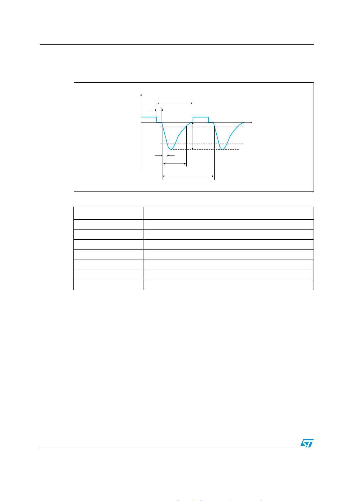
The most severe negative pulse is pulse 1 (Figure 3). It can reach -100 V during 2 ms and a
peak current of 10 A in shorted conditions.
Figure 3. ISO 7637-2 pulse 1
t
U
t
3
2
0.1xU
S
U
0.9xU
S
t
r
t
d
t
1
Table 3. Parameter values for test pulse 1
S
t
Parameter 12 V system
U
s
R
i
t
d
t
r
(1)
t
1
t
2
(2)
t
3
1. Period t1 shall be chosen such that the DUT is correctly initialized before the application of the next pulse.
2. Period t3 is the smallest possible time necessary between this disconnection of the supply source and the
application of the pulse.
-75 V to -100 V
10 Ω
2 ms
1 µs
0.5 s to 5 s
200 ms
<100 µs
4/15 Doc ID 018589 Rev 1
Page 5
AN3361 Definition of the electrical transients and tests
Pulse 3a (Figure 4) is specified at -150 V but with 50 Ω series resistor and 100 ns duration
which is far less energy than for pulse 1. This means that, if the Schottky diode specification
is compliant with pulse 1, pulse 3a will be covered as well.
Figure 4. ISO 7637-2 pulse 3a
0.1xU
0.9xU
t
5
U
S
S
S
t
r
t
U
t
4
1
t
Table 4. Parameter values for test pulse 3a
Parameter 12 V system
U
s
R
i
t
d
t
r
t
1
t
4
t
5
U
d
-112 V to -150 V
t
S
50 Ω
0.1 µs
5 ns
100 µs
10 ms
90 ms
Doc ID 018589 Rev 1 5/15
Page 6

Choosing the appropriate Schottky diode AN3361
2 Choosing the appropriate Schottky diode
Schottky diode choice for reverse battery protection is determined by the electronic module
normal operating current on the one hand, and the need to pass the ISO 7637-2 pulse tests
on the other. Each module has its own normal operating current, which is defined by its
characteristics. So here we will consider only the method to choose an appropriate Schottky
diode to meet the ISO 7637-2 requirements.
2.1 Load-dump surge compatibility criteria
The first criterion is the compatibility between surge current and I
datasheet.
2.1.1 Load-dump peak current calculation
Figure 6 shows the current shape through the Schottky diode during a load-dump surge
according to the schematic described in Figure 5.
Figure 5. Pulse 5b surge test schematic
Schottky diode
I
R = 0.5iΩ
Pulse 5b:
V =13.5 V
bat
V = [24-48 V]
g
t = 300 ms
ps
specified in the diode
FSM
p
V
F
V
cl
Electronic module
6/15 Doc ID 018589 Rev 1
Page 7

AN3361 Choosing the appropriate Schottky diode
I
p
10.0 V/div
-30.20 V ofst
10.0 V/div
-30.00 V ofst
50.0 ms/div
50.0 kS 100 kS/s
Stop 16.8 V
Edge Positive
Figure 6. Current and voltage at the transient suppressor side (with a 24 V Vbr
clamping device and V
max
C1
= 36V)
g
V
cl
C2
Measure
value
status
10.0 V/div
-30.20 V ofst
max
P1:max(C1)
10.0 V/div
-30.00 V ofst
29.9 V
I
p
P2:max(C2)
35.9 V
P3:mean(F1) P4:rise@Iv(C3) P5:--- P6:---
50.0 ms/div
50.0 kS 100 kS/s
The equations below apply to the circuit shown in Figure 5.
Equation 1
VVV +=
batgsurge
IR)(IVVV ++=
pipFclsurge
·IRV)(IV +=
pdT0pF
The calculation of V
and Rd is explained in the application note AN604: “Calculation of
T0
conduction losses in a power rectifier”. Values are provided in the datasheets.
Then:
Stop 16.8 V
Edge Positive
Equation 2
VVV
−−
I
=
p
In the example presented in Figure 6 the generator surge voltage (V
T0clsurge
RR
+
id
) is 36 V, its internal
g
series resistor is 0.5 Ω, the battery voltage is 12 V and the protection voltage clamping level
of the protection device is 29.9 V. The diode dynamic resistor R
As V
T0
<< V
- Vcl the above relation can be simplified to:
surge
is 0.009 Ω.
d
Equation 3
29.912)(36
I
=
p
So the peak current I
−+
0.50.009
+
is equal to 35.56 A.
p
Doc ID 018589 Rev 1 7/15
Page 8

Choosing the appropriate Schottky diode AN3361
2.1.2 Method to compare Ip and I
I
is the maximum peak current of a sinusoidal waveform pulse during 10 ms. The load-
FSM
dump peak current can be approximated with a constant and an exponential waveform
pulse. To compare both peak currents, I
calculate the equivalent sinusoidal surface of the exponential waveform in order to deduce
the equivalent pulse duration.
The surge load-dump surface is modeled using the following equation:
Equation 4
t
0
Where I
0
Equation 5
t
sin
=
∫
0
The equivalent pulse duration is t
Equation 6
SS =
surgesin
∞
1
+=
0surge
−−
)1t(t
τ
0
∫∫
t
1
dt·eI·dtIS
is the maximum load-dump current. The equivalent sinusoidal waveform is:
2ð
2·t
)dtt
sin
sin
·sin(IS
0sin
FSM
FSM
, since:
and load-dump peak current, one method is to
Then:
Equation 7
π
t
=
2
Where
Equation 8
t1t
−
I
0
2
=τ
ln2
)t(
+τ
1sin
8/15 Doc ID 018589 Rev 1
Page 9

AN3361 Choosing the appropriate Schottky diode
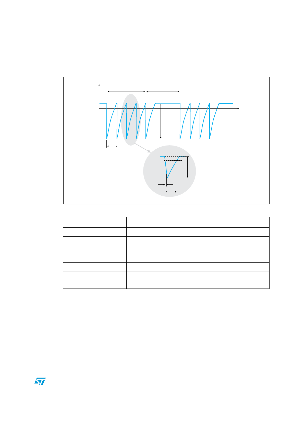
Figure 7. Equivalent sinusoidal surface of clamped load-dump surge surface
I0
2.1.3 I
t1
I (t)
surge
I
(ti)
sin
40
30
I0/2
20
10
t
sin
0
0 0.1 0.2
tI0/2
t, ti
In our example the equivalent sinusoidal waveform pulse time duration t
value versus pulse time
FSM
Using the equations:
Equation 9
4
I
x t = C
3
I
x t = C
2
I
x t = C
for t
ste
ste
ste
sin
for 20 µs <t
for t
sin
>10 ms
sin
<20 ms
>10 ms
In the example for the STPS20L60C in Figure 7, as the pulse duration t
following law from Equation 9 can be used:
is 140 ms.
sin
is 140 ms, the
sin
Equation 10
4
FSM@ tsin
10·10ItI
×=×
FSMsin
34
−
Where:
I
is the non repetitive forward surge current given in the data sheet.
FSM
I
FSM @ t sin
For the example of Figure 6, the I
is the non repetitive forward surge current for a pulse duration t
= 220 A
FSM
Equation 11
−
43
I10·10
×
I
FSM@140ms
I
FSM@140ms
4
=
4
=
140·10
The equivalent peak current is I
The peak current delivered by the test system is I
I
@140 ms. So the STPS20L60C meets the ISO 7637-2 requirements.
FSM
FSM
t
sin
−
43
22010·10
×
3
−
@140 ms = 113.73 A.
FSM
= 35.56 A and it is less than
p
Doc ID 018589 Rev 1 9/15
sin
.
Page 10

Choosing the appropriate Schottky diode AN3361
Ta bl e 5 gives a matrix of which Schottky diode is compatible with load-dump surge (pulse
5b) depending on surge voltage level and with the conditions: V
= 13.5 V, Ri = 0.5 Ω and
bat
with load-dump surge duration of 300 ms.
Table 5. Which Schottky diodes are good for which load-dump surge level
Pulse 5b load-dump surge voltage (Vg) 2430364248
STPS160AY Yes
STPS3L60SY Yes Yes
STPS20L60CGY Yes Yes Yes Yes Yes
STPS1H100UY Yes
STPS2H100UY Yes Yes
STPS5H100BY Yes Yes Yes
STPS8H100GY Yes Yes Yes Yes Yes
2.2 Most severe negative surge compatibility criteria
Now if we consider pulse 1 as shown in Figure 3, things are different since the Schottky
diode is reverse polarized.
For instance, the voltage applied on a diode with a maximum repetitive reverse voltage
(V
) of 100 V will be VR = -113.5 V (VR = V
RRM
+ Vc due to the charge of the capacitor).
surge
Figure 8. Example of application with pulse 1 using an STPS5H100BY
STPS5H100BY
I
Pulse 1:
V = 13.5 V
bat
V = -100
surge
R = 10
t = 2 ms
Ω
i
p
V
RRM
Electronic module
V = 13.5 V
c
10/15 Doc ID 018589 Rev 1
Page 11

AN3361 Choosing the appropriate Schottky diode
A Pspice simulation shows the power involved in an STPS5H100BY, for example, as shown
in Figure 10, according to the schematic of Figure 9.
Figure 9. Pspice model of Pulse 1 surge test using STPS5H100BY Schottky diode
STPS5H100 Pspice Model
R1
10
V1 = 0
V2 = -100
TD1 = 0.1 m
TC1 = 400 n
TD2 = 0.1004 m
TC2 = 0.85 m
V2
ISO7637-2 Pulse 1 Pspice Model
Figure 10. Pspice simulation result
W
200
2
100
W
W
0
Diode dissipation power
D3
D5
V3
-
100
0
+
C1
1000 u
I = 13.5
C
Probe Cursor
A1 = 103.192 u, 118.574
A2 = 222.340 u, 1.3069
dif = -119.149 u, 117.267
I1
1
>
SEL>
W
-100
120V
2
1
V (I 1: +, D3 : C)* I ( V3: +)
2. 0A
Diode reverse voltage
80V
40V
1. 0A
>
0V
>
0A
0s 0. 1ms 0. 2ms 0. 3ms 0. 4ms 0. 5ms 0. 6ms 0. 7ms 0. 8ms 0.
1
V (I 1: +, D3 : C)
Diode reverse current
2 I(V3)
9ms 1. 0ms
Time
The blue curve in Figure 10 is the power dissipated in the diode avalanche. It is a triangular
shape curve with a peak power at 118 W during 120 µs. This waveform is equivalent to a
59 W square shape pulse of 120 µs duration.
In order to evaluate if the diode is able to dissipate this energy in the avalanche, two
elements are relevant:
● P
● P
(1 µs, Tj = 25° C) is the repetitive peak avalanche power
ARM
ARM(Tp
)/ P
(1 µs, Tj = 25 °C) curve Figure 11.
ARM
Doc ID 018589 Rev 1 11/15
Page 12

Choosing the appropriate Schottky diode AN3361
In the example, we have selected the STPS5H100BY where:
P
(1 µs, Tj = 25 °C) = 7200 W.
ARM
The derating curve Figure 11 shows the equivalent avalanche power the STPS5H100BY is
able to dissipate is 0.035 · P
(1 µs, Tj = 25 °C) = 252 W
ARM
Therefore in this example the STPS5H100BY meets the ISO 7637-2 requirements and
ensures a good reverse battery protection.
Figure 11. Normalized avalanche power derating versus pulse duration for
STPS5H100BY
P(t)
ARM p
P (1µs)
ARM
1
0.1
0.035
0.01
t (µs)
0.001
0.10.01 1
10 100
120 µs
p
1000
Note: The derating curve for STPS5H100BY can be found as Figure 3 in the datasheet for this
device.
Ta bl e 6 indicates which Schottky diode can withstand Pulse 1 of ISO 7637-2 standard.
Table 6. Compliance of Schottky diodes with ISO 7637-2 Pulse 1
Pulse 1 surge voltage (V) Vs = -100 V
STPS2H100UY Yes
STPS5H100BY Yes
STPS8H100GY Yes
Ta bl e 6 shows that only a few Schottky diodes can handle this constraint.
12/15 Doc ID 018589 Rev 1
Page 13

AN3361 Conclusion
3 Conclusion
Protecting automotive electronic modules from polarity inversion due to poor battery
handling and load-dump surge during battery disconnection while the alternator is still
charging usually involves the use of diodes, especially Schottky diodes rather than bipolar
ones because of their better performance in direct conduction. The choice must consider
the worst-case surge conditions of ISO 7637-2 which are pulses 1 and 5b.
Usually Schottky diodes with a breakdown voltage of 150 V are preferred for this application.
This article shows that a breakdown voltage of 100 V may be selected to withstand
avalanche mode during the negative pulse 1 test (starting from a 2 A Schottky type). This
results in the saving of power during direct conduction.
Note: ST parts numbers listed in this application note were given as examples and are not an
exhaustive list. Please contact your sales or marketing representative for more automotive
grade rectifier devices.
Doc ID 018589 Rev 1 13/15
Page 14

Revision history AN3361
4 Revision history
Table 7. Document revision history
Date Revision Changes
09-Sep-2011 1 Initial release.
14/15 Doc ID 018589 Rev 1
Page 15

AN3361
Please Read Carefully:
Information in this document is provided solely in connection with ST products. STMicroelectronics NV and its subsidiaries (“ST”) reserve the
right to make changes, corrections, modifications or improvements, to this document, and the products and services described herein at any
time, without notice.
All ST products are sold pursuant to ST’s terms and conditions of sale.
Purchasers are solely responsible for the choice, selection and use of the ST products and services described herein, and ST assumes no
liability whatsoever relating to the choice, selection or use of the ST products and services described herein.
No license, express or implied, by estoppel or otherwise, to any intellectual property rights is granted under this document. If any part of this
document refers to any third party products or services it shall not be deemed a license grant by ST for the use of such third party products
or services, or any intellectual property contained therein or considered as a warranty covering the use in any manner whatsoever of such
third party products or services or any intellectual property contained therein.
UNLESS OTHERWISE SET FORTH IN ST’S TERMS AND CONDITIONS OF SALE ST DISCLAIMS ANY EXPRESS OR IMPLIED
WARRANTY WITH RESPECT TO THE USE AND/OR SALE OF ST PRODUCTS INCLUDING WITHOUT LIMITATION IMPLIED
WARRANTIES OF MERCHANTABILITY, FITNESS FOR A PARTICULAR PURPOSE (AND THEIR EQUIVALENTS UNDER THE LAWS
OF ANY JURISDICTION), OR INFRINGEMENT OF ANY PATENT, COPYRIGHT OR OTHER INTELLECTUAL PROPERTY RIGHT.
UNLESS EXPRESSLY APPROVED IN WRITING BY TWO AUTHORIZED ST REPRESENTATIVES, ST PRODUCTS ARE NOT
RECOMMENDED, AUTHORIZED OR WARRANTED FOR USE IN MILITARY, AIR CRAFT, SPACE, LIFE SAVING, OR LIFE SUSTAINING
APPLICATIONS, NOR IN PRODUCTS OR SYSTEMS WHERE FAILURE OR MALFUNCTION MAY RESULT IN PERSONAL INJURY,
DEATH, OR SEVERE PROPERTY OR ENVIRONMENTAL DAMAGE. ST PRODUCTS WHICH ARE NOT SPECIFIED AS "AUTOMOTIVE
GRADE" MAY ONLY BE USED IN AUTOMOTIVE APPLICATIONS AT USER’S OWN RISK.
Resale of ST products with provisions different from the statements and/or technical features set forth in this document shall immediately void
any warranty granted by ST for the ST product or service described herein and shall not create or extend in any manner whatsoever, any
liability of ST.
ST and the ST logo are trademarks or registered trademarks of ST in various countries.
Information in this document supersedes and replaces all information previously supplied.
The ST logo is a registered trademark of STMicroelectronics. All other names are the property of their respective owners.
© 2011 STMicroelectronics - All rights reserved
STMicroelectronics group of companies
Australia - Belgium - Brazil - Canada - China - Czech Republic - Finland - France - Germany - Hong Kong - India - Israel - Italy - Japan -
Malaysia - Malta - Morocco - Philippines - Singapore - Spain - Sweden - Switzerland - United Kingdom - United States of America
www.st.com
Doc ID 018589 Rev 1 15/15
 Loading...