


AN3357
Application note
HSP061-8M16 high speed line protection on HDMI 1.4 link
Introduction
This Application note presents the HSP061-8M16 and its capability to protect HDMI 1.3 and
HDMI 1.4 TMDS lines.
The HDMI interface is provided for transmitting digital television audiovisual signals from
DVD players, set-top- boxes and other source to television sets and other video displays.
HSP061-8M16 has been developed to be compliant with:
■ HDMI version 1.4 standard knowing the key point is the capability to transfer data with a
maximum rate of 3.4 Gbps per channel without distortion. This leads the HSP061-8M16
to have a large bandwidth, to pass fast voltage slope and to keep the 100 Ω line
impedance, HSP061-8M16 is used on the TMDS line.
■ IEC 61000-4-2 level 4 (15 kV contact discharge)
April 2011 Doc ID 018580 Rev 1 1/10
www.st.com
Location for HSP061-8M16 AN3357
1 Location for HSP061-8M16
Many PCB parasitic elements may degrade the overall ESD performance of a system. The
recommendations below are aimed at optimizing ESD protection device placement and the
PCB layout to reach the best ESD performance possible.
The layout shown in Figure 1 may induce parasitic inductances responsible for artificial
overvoltages directly applied on the IC to be protected.
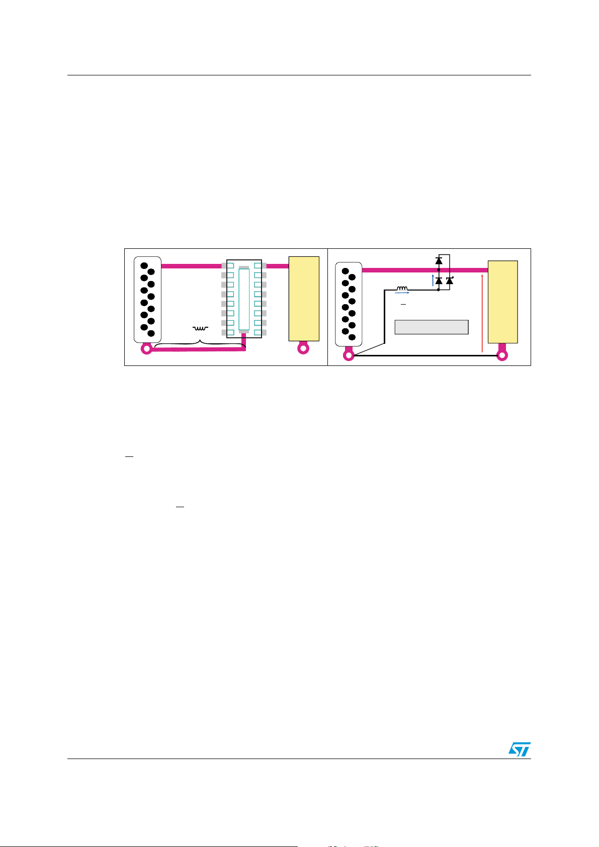
Figure 1. Non-optimized location for
HSP061-8M16
16
1
16
2
15
3
14
4
Via to GND
13
G
N
5
12
D
6
11
10
7
8
=
9
Via to
GND
IC to
protect
Figure 2. Significant overvoltages due
to non-optimal location of
HSP061-8M16
V
di
L
dt
ESD surge is 15 kV with 1 ns
rise time, this leads to 71 A/ ns
GND layer
IC to
protect
V
IC
Via to
GND
A very simple calculation shows that for a 15 kV ESD contact surge according to
IEC61000-4-2, the overvoltage due to parasitic inductances may be really significant, as
shown in Figure 2. This test is done with a contact discharge as the air discharge waveform
is not defined in the IEC 61000-4-2 specification. Assuming that each inductance value is 5
nH (corresponds to metal track 5 mm long):
di
= 71 A/ns
dt
then the overvoltage seen by the IC is:
V = V +
IC
V = V + 355 V
IC
di
L·
dt
This parasitic inductance must be reduced as much as possible by shortening the ground
path return to the GND via.
To avoid ESD propagation on the PCB, the ESD protection must be placed as close as
possible to the ESD source with the layout given in the datasheet.
The layout given in the datasheet reduces parasitic inductance. It is important to connect the
connector on one side of the HSP and the transceiver on the other side. The GND via on
both sides must be used.
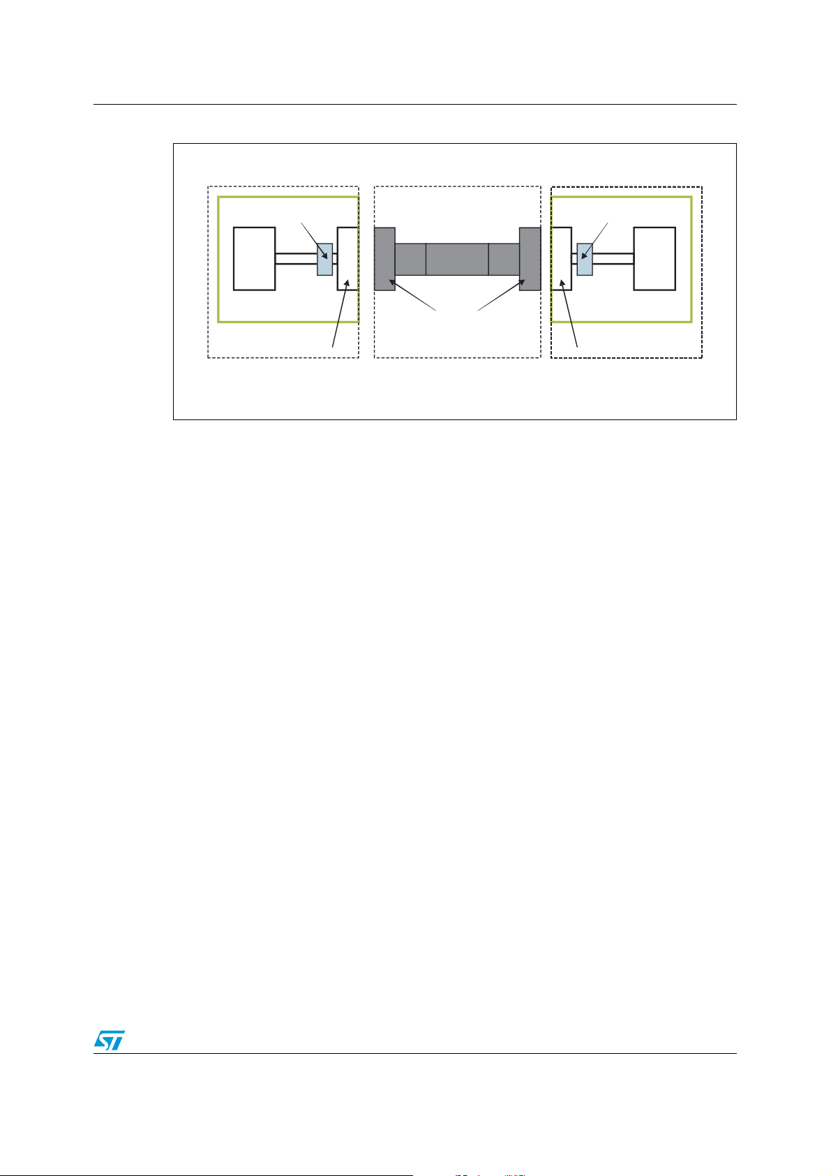
As ESD stress can be propagated on both sides of the cable, a protection device on each
end of the cable is required.
2/10 Doc ID 018580 Rev 1
AN3357 Location for HSP061-8M16
Figure 3. Protection location on HDMI equipment
Protection
Tx
Board
Receptacle
(connector)
Source device (i.e., DVD)
Wire
Plug
Cable assembly
Protection
Rx
Board
Receptacle
(connector)
Sink device (Display)
Doc ID 018580 Rev 1 3/10
HSP061-8M16 topology AN3357
2 HSP061-8M16 topology
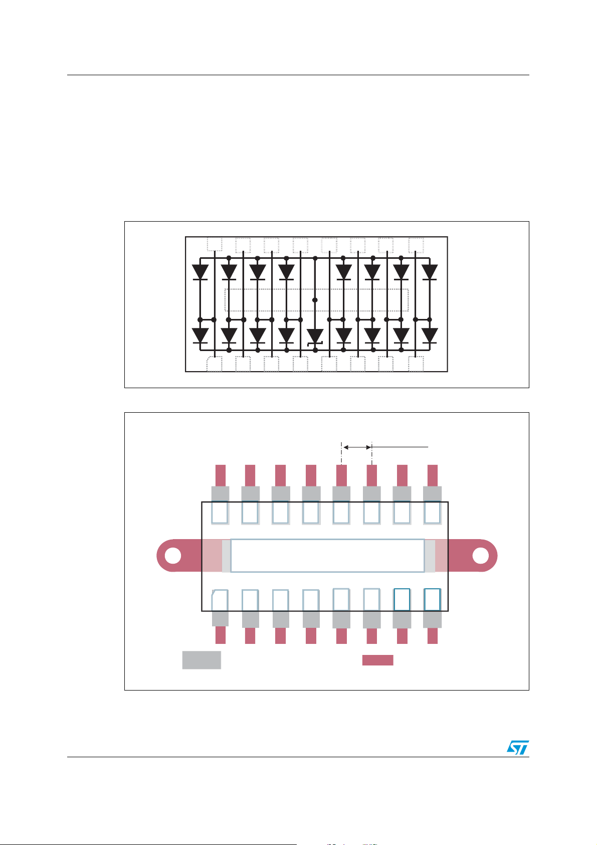
HSP061-8M16 is packaged in µQFN-16L (3.3 mm x 1.5 mm) to protect eight high speed
lines (see Figure 4). This package keeps the 100 Ω differential impedance on HDMI
(Figure 5).
The device is rated V
min = 6 V @ 1 mA with a low typical leakage current of
BR
0.1 nA @ 25 °C.
Figure 4. HSP061-8M16 topology
Out 4
Out 3
Out 2
Out 1
16
15
14
13
In 1
1
In 2
3
2
In 3
4
In 4
Figure 5. HSP061-8M16 PCB footprint
Out 5
In 5
12
5
Out 6
In 6
11
6
Out 7
10
7
In 7
400 µm
Out 8
In 8
9
GND
on
Tab
8
Via to
GND
16
16
1
15
2
Footprint pad PC B tracks
13
GND
4
3
For further information refer to the product datasheet for HSP061-8M16.
4/10 Doc ID 018580 Rev 1
121411
5
6
10
7
9
Via to
GND
8
AN3357 Characteristics related to HDMI 1.4
3 Characteristics related to HDMI 1.4
Protection bandwidth must be large enough to be transparent when a high bit rate is
transferred on the line. The equation below give the relationship between lines, pixels, color
depth and bit rate per channel:
Lane data rate = (H_total_pixels) × (V_total_lines) ×
Table 1. Sample characteristics
⎛⎞Color_depth
⎜
⎝
3
× (Frame_rate) ×
⎜
⎠
10
8
CEA video
code
Video format
Horizontal
total pixel
per line
Vertical
total lines
per frame
Frame
rate (Hz)
Color
depth
(bits)
HDMI
data rate
(Gbps)
Lane
data rate
(Gbps)
24 4.46 1.49
30 5.57 1.86
16 1920 x 1080p 2200 1125 60
36 6.68 2.23
48 8.91 2.97
Considering the protection device is equivalent to an RC circuit, the relationship between
the required cut-off frequency (f
f = 0.875 × (lane data rate)
c
min
) and lane data rate is:
c
For instance, with a 3.4 Gbps data rate:
f = 0.875 × 3.4 Gbps = 2.98 GHz
c
min 3.4 Gbps
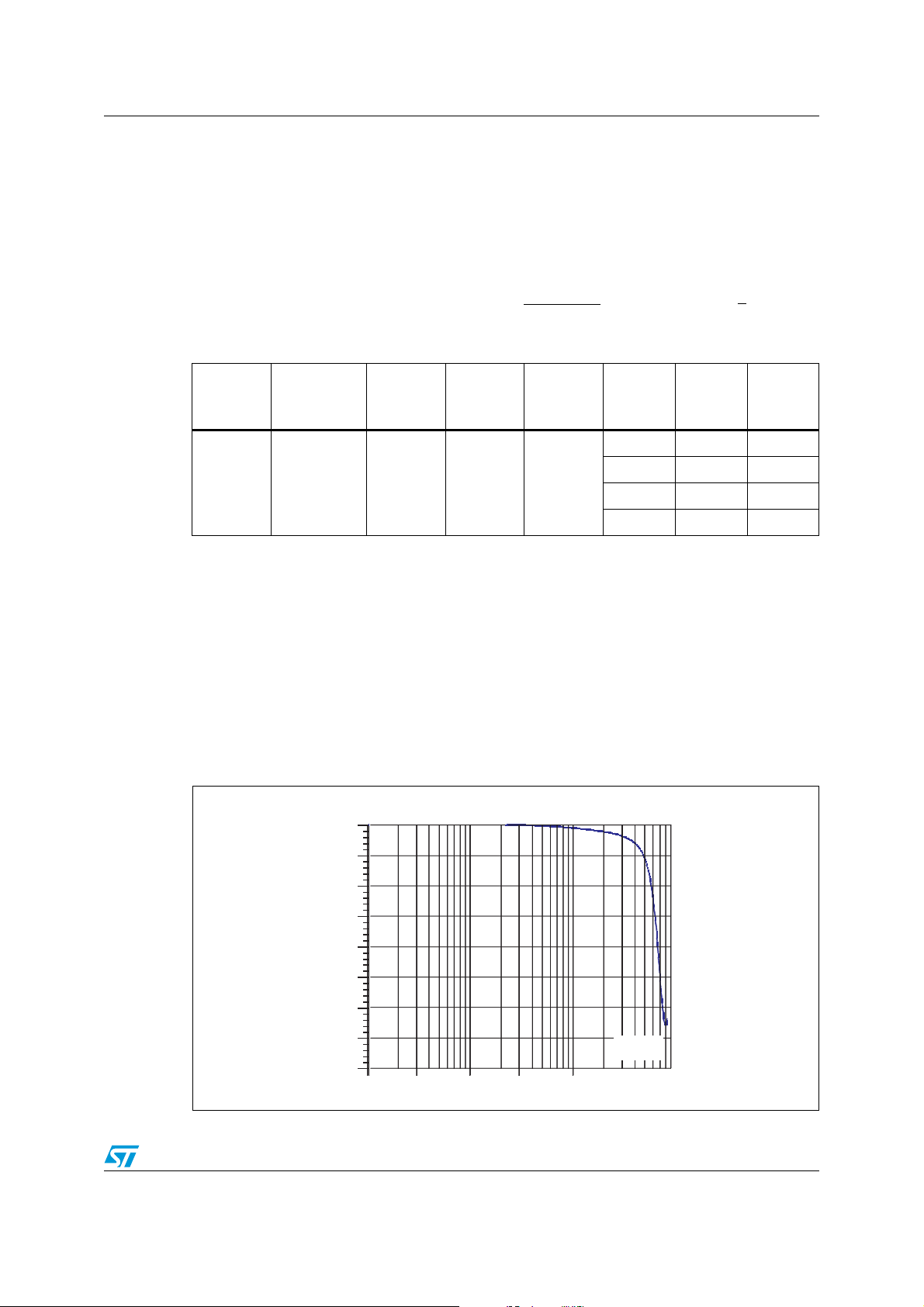
Figure 6 shows the cut-off frequency of the HSP061-8M16 is 6.3 GHz which is high enough
to manage HDMI signals at 3.4 Gbps.
Figure 6. S21 attenuation measurement
db
0
-1
-2
-3
-4
-5
-6
-7
-8
10MHz 30MHz 100MHz 300MHz 1GHz 3GHz
Doc ID 018580 Rev 1 5/10
F (Hz)

Characteristics related to HDMI 1.4 AN3357
Figure 7. Differential impedance
tr = 200 ps (10% - 90%)
12.5 Ω /div
Z
= 100 Ω
0Diff
-
Figure 7 shows the differential impedance measured with the “Time Domain Reflectometry”
method. This method consists of sending a pulse with a short rise time (200 ps between
10% and 90% for HDMI) and to measure the reflected pulse. This gives the impedance of
the line along the signal path.
The HDMI standard requires 100 Ω ±15% differential impedance (between 85 Ω and
115 Ω). As shown on Figure 7, TDR measurement on HSP061-8M16 gives an impedance
between 93 Ω and 100 Ω. These values are in accordance with the HDMI standard.
The eye diagrams defined in the HDMI standard are related to bit rate of the signal and to
location (source or sink). There are more constraints on the source side, this is why we have
chosen this one on the datasheet. The duration of the eye corresponds to a bit time. This
diagram visualizes signal duration, synchronization, overshoot and capability of the signal to
move from one state to another one. The key point for protection is to be sure there is no
slow down effect. Figure 8 shows the eye diagram for a 3.4 Gbps signal. This measurement
is done directly on the HSP061-8M16 to avoid PCB measurement effects. Measurement
shows a large safety margin between the eye pattern and the signal.
Figure 8. Eye diagram at 3.4Gbps
Vertical : 200 mV / div
Horizontal : 50 ps / div
6/10 Doc ID 018580 Rev 1

AN3357 Characteristics related to HDMI 1.4
Figure 9. IEC 61000-4-2 response
50 V / div
20 ns / div
20 GS / s
ESD peak volatge VCL@30 ns VCL@60 ns
+8 kV
-8 kV
+168 V 14 V 15 V
-169 V -7 V -7 V
The goal of a protection device is to protect against parasitic disturbances. HDMI 1.4
standard specifies a 8 kV contact discharge requirement according to IEC 61000-4-2. The
test must be performed 5 times with 1 second during each shot.
In Figure 9 shows the ESD measurement when applied to HSP061-8M16. After a first short
spike, the clamping voltage is limited to less than 20 V at 30 ns and less than 10 V at 60 ns
instead of 8 kV.
There is no ageing phenomenon and the protection remains efficient whatever the number
of surges. It is important to keep in mind most of the integrated circuits are ESD rated
between 500 V and 2 kV (human body model) thanks to internal protection.
Doc ID 018580 Rev 1 7/10
Layout considerations AN3357
4 Layout considerations
PCB layout must be optimized to take advantage of all performances of the HSP061-8M16.
For ESD protection efficiency, the HSP061-8M16 must be located as close as possible to
the connector. This will avoid disturbance propagation to other components through the
coupling effect.
To avoid the inductance effect of PCB tracks, it is required to go directly from the connector
to the HSP061-8M16 and then after to go to the HDMI circuit. Vias to connect the ground
pins of HSP061-8M16 to the ground plane must be as many as possible and placed as
close as possible to the protection device to reduce parasitic inductance on the ground
return path. Vias to connect ground plane and the connector can be located on both sides of
the connector.
To be compliant with HDMI requirements, differential pairs must be designed with 100 Ω
differential impedance from the connector to the IC. The length of each line in the same
differential pair must be equal to minimize intra pair skew. Length of lines in different
differential pair must also be as equal as far as possible to minimize inter pair skew. Track
width must be calculated depending on PCB characteristics (relative permittivity, spacing,
number of layers…)
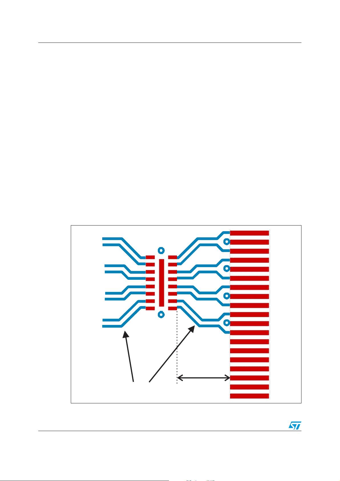
Figure 10 shows an example of PCB layout for HSP061-8M16 with an HDMI type A SMD
connector..
Figure 10. Layout example for HSP061-8M16 with HDMI type A SMD connector
100 differential pairsΩ
As short as possible
8/10 Doc ID 018580 Rev 1

AN3357 Conclusion
Figure 11 shows an example of PCB layout for HSP061-8M16 with an HDMI type C SMD
connector
Figure 11. Layout example for HSP061-8M16 with HDMI type C SMD connector
100 differential pairsΩ
5 Conclusion
The HSP061-8M16 is perfectly in line with the IEC61000-4-2 requirements and is fully
compliant with HDMI 1.4 standards and also with most of the other high speed data lines
lines (Ethernet, DisplayPort, USB3.0, SATA…)
6 Revision history
Table 2. Document revision history
Date Revision Changes
19-Apr-2011 1 Initial release.
As short as possible
Doc ID 018580 Rev 1 9/10

AN3357
Please Read Carefully:
Information in this document is provided solely in connection with ST products. STMicroelectronics NV and its subsidiaries (“ST”) reserve the
right to make changes, corrections, modifications or improvements, to this document, and the products and services described herein at any
time, without notice.
All ST products are sold pursuant to ST’s terms and conditions of sale.
Purchasers are solely responsible for the choice, selection and use of the ST products and services described herein, and ST assumes no
liability whatsoever relating to the choice, selection or use of the ST products and services described herein.
No license, express or implied, by estoppel or otherwise, to any intellectual property rights is granted under this document. If any part of this
document refers to any third party products or services it shall not be deemed a license grant by ST for the use of such third party products
or services, or any intellectual property contained therein or considered as a warranty covering the use in any manner whatsoever of such
third party products or services or any intellectual property contained therein.
UNLESS OTHERWISE SET FORTH IN ST’S TERMS AND CONDITIONS OF SALE ST DISCLAIMS ANY EXPRESS OR IMPLIED
WARRANTY WITH RESPECT TO THE USE AND/OR SALE OF ST PRODUCTS INCLUDING WITHOUT LIMITATION IMPLIED
WARRANTIES OF MERCHANTABILITY, FITNESS FOR A PARTICULAR PURPOSE (AND THEIR EQUIVALENTS UNDER THE LAWS
OF ANY JURISDICTION), OR INFRINGEMENT OF ANY PATENT, COPYRIGHT OR OTHER INTELLECTUAL PROPERTY RIGHT.
UNLESS EXPRESSLY APPROVED IN WRITING BY AN AUTHORIZED ST REPRESENTATIVE, ST PRODUCTS ARE NOT
RECOMMENDED, AUTHORIZED OR WARRANTED FOR USE IN MILITARY, AIR CRAFT, SPACE, LIFE SAVING, OR LIFE SUSTAINING
APPLICATIONS, NOR IN PRODUCTS OR SYSTEMS WHERE FAILURE OR MALFUNCTION MAY RESULT IN PERSONAL INJURY,
DEATH, OR SEVERE PROPERTY OR ENVIRONMENTAL DAMAGE. ST PRODUCTS WHICH ARE NOT SPECIFIED AS "AUTOMOTIVE
GRADE" MAY ONLY BE USED IN AUTOMOTIVE APPLICATIONS AT USER’S OWN RISK.
Resale of ST products with provisions different from the statements and/or technical features set forth in this document shall immediately void
any warranty granted by ST for the ST product or service described herein and shall not create or extend in any manner whatsoever, any
liability of ST.
ST and the ST logo are trademarks or registered trademarks of ST in various countries.
Information in this document supersedes and replaces all information previously supplied.
The ST logo is a registered trademark of STMicroelectronics. All other names are the property of their respective owners.
© 2011 STMicroelectronics - All rights reserved
STMicroelectronics group of companies
Australia - Belgium - Brazil - Canada - China - Czech Republic - Finland - France - Germany - Hong Kong - India - Israel - Italy - Japan -
Malaysia - Malta - Morocco - Philippines - Singapore - Spain - Sweden - Switzerland - United Kingdom - United States of America
www.st.com
10/10 Doc ID 018580 Rev 1
 Loading...