


AN3310
Application note
Updating firmware in STM32L1xx microcontrollers through
in-application programming using the USART
Introduction
An important requirement for most Flash-memory-based systems is the ability to update the
firmware when installed in the end product. This ability is referred to as in-application
programming (IAP). The purpose of this application note is to provide general guidelines for
creating an IAP application.
The STM32L1xx microcontroller can run user-specific firmware to perform IAP of the
microcontroller-embedded Flash memory. This feature allows the use of any type of
communication protocol for the reprogramming process. The USART is the example used in
this application note.
January 2012 Doc ID 18201 Rev 2 1/19
www.st.com

Contents AN3310
Contents
1 IAP overview . . . . . . . . . . . . . . . . . . . . . . . . . . . . . . . . . . . . . . . . . . . . . . . 3
1.1 Principle . . . . . . . . . . . . . . . . . . . . . . . . . . . . . . . . . . . . . . . . . . . . . . . . . . . 3
1.2 IAP driver description . . . . . . . . . . . . . . . . . . . . . . . . . . . . . . . . . . . . . . . . . 3
2 Running the IAP driver . . . . . . . . . . . . . . . . . . . . . . . . . . . . . . . . . . . . . . . 6
2.1 HyperTerminal configuration . . . . . . . . . . . . . . . . . . . . . . . . . . . . . . . . . . . 6
2.2 Executing the IAP driver . . . . . . . . . . . . . . . . . . . . . . . . . . . . . . . . . . . . . . . 7
3 IAP driver menu . . . . . . . . . . . . . . . . . . . . . . . . . . . . . . . . . . . . . . . . . . . . . 8
3.1 Downloading an image to the internal Flash memory . . . . . . . . . . . . . . . . 8
3.2 Uploading an image from the internal Flash memory . . . . . . . . . . . . . . . . 9
3.3 Executing the new program . . . . . . . . . . . . . . . . . . . . . . . . . . . . . . . . . . . . 9
3.4 Disabling the write protection . . . . . . . . . . . . . . . . . . . . . . . . . . . . . . . . . . . 9
4 STM32L1xx IAP implementation summary . . . . . . . . . . . . . . . . . . . . . . 10
5 User program conditions . . . . . . . . . . . . . . . . . . . . . . . . . . . . . . . . . . . . 12
6 Firmware updates . . . . . . . . . . . . . . . . . . . . . . . . . . . . . . . . . . . . . . . . . . 13
7 How to place FLASH programming functions into internal
SRAM/FLASH 14
8 Memory write protection . . . . . . . . . . . . . . . . . . . . . . . . . . . . . . . . . . . . . 15
9 Dual bank feature for high-density devices . . . . . . . . . . . . . . . . . . . . . 16
10 Revision history . . . . . . . . . . . . . . . . . . . . . . . . . . . . . . . . . . . . . . . . . . . 18
2/19 Doc ID 18201 Rev 2

AN3310 IAP overview
1 IAP overview
Ultra low power medium-density devices are STM32L151xx and STM32L152xx
microcontrollers where the Flash memory density ranges between 64 and 128 Kbytes. Ultra
low power medium-density devices are implemented in the STMicroelectronics
STM32L152-EVAL evaluation board.
Ultra low power medium-density plus devices are STM32L151xx, STM32L152xx and
STM32L162xx microcontrollers where the Flash memory density is 256 Kbytes.
Ultra low power high-density devices are STM32L151xx, STM32L152xx and STM32L162xx
microcontrollers where the Flash memory density is 384 Kbytes. Ultra low power highdensity devices are implemented in the STMicroelectronics STM32L152D-EVAL evaluation
board.
1.1 Principle
You should program the IAP driver to the Flash memory base address via the JTAG/SWD
interface using the development toolchain of your choice or the factory-embedded boot
loader in the System memory area.
The IAP driver uses the USART to:
● Download a binary file from the HyperTerminal to the STM32L1xx's internal Flash
memory.
● Upload the STM32L1xx's internal Flash memory content (starting from the defined user
application address) into a binary file.
● Execute the user program.
1.2 IAP driver description
The IAP driver contains the following set of source files:
● main.c: where the USART initialization and RCC configuration are set. A main menu is
then executed from the menu.c file.
● menu.c: contains the main menu routine. The main menu gives the options of
downloading a new binary file, uploading internal Flash memory, executing the binary
file already loaded and disabling the write protection of the pages where the user loads
his/her binary file (if they are write-protected).
● flash_if.c: contains write, erase and disable write protection of the internal Flash
memory.
● common.c: contains functions related to read/write from/to the USART peripheral.
● ymodem.c: is used to receive/send the data from/to the HyperTerminal application
using the YMODEM protocol
“Failed to receive the file” error message is displayed. If the data is received
(a)
. In the event of a failure when receiving the data, the
a. The Ymodem protocol sends data in 1024-byte blocks. An error check is performed in data blocks transmitted
to the STM32L1xx’s internal RAM to compare the transmitted and received data. Blocks unsuccessfully
received are acknowledged with an NAK (Negative Acknowledgement). For more details about the Ymodem
protocol, refer to existing documentation.
Doc ID 18201 Rev 2 3/19

IAP overview AN3310
successfully, it is programmed into the internal Flash memory from the appropriate
address. A comparison between internal RAM contents and internal Flash memory
contents is performed to check the data integrity. If there is any data discrepancy, the
“Verification failed” error message is displayed. Other error messages are also
displayed when the image file size is greater than the allowed memory space and when
the user aborts the task.
● STM32L1xx Standard Peripherals Library.
The user can choose to either go to the user application or execute the IAP for
reprogramming purposes by pressing a push-button connected to a pin.
● Not pressing the push-button at reset switches to the user application
● Pressing the push-button at reset displays the IAP main menu
Refer to Table 1. STM32L1xx IAP implementation for more details about the STM32L15xx-
EVAL board push-button used to enter the IAP mode.
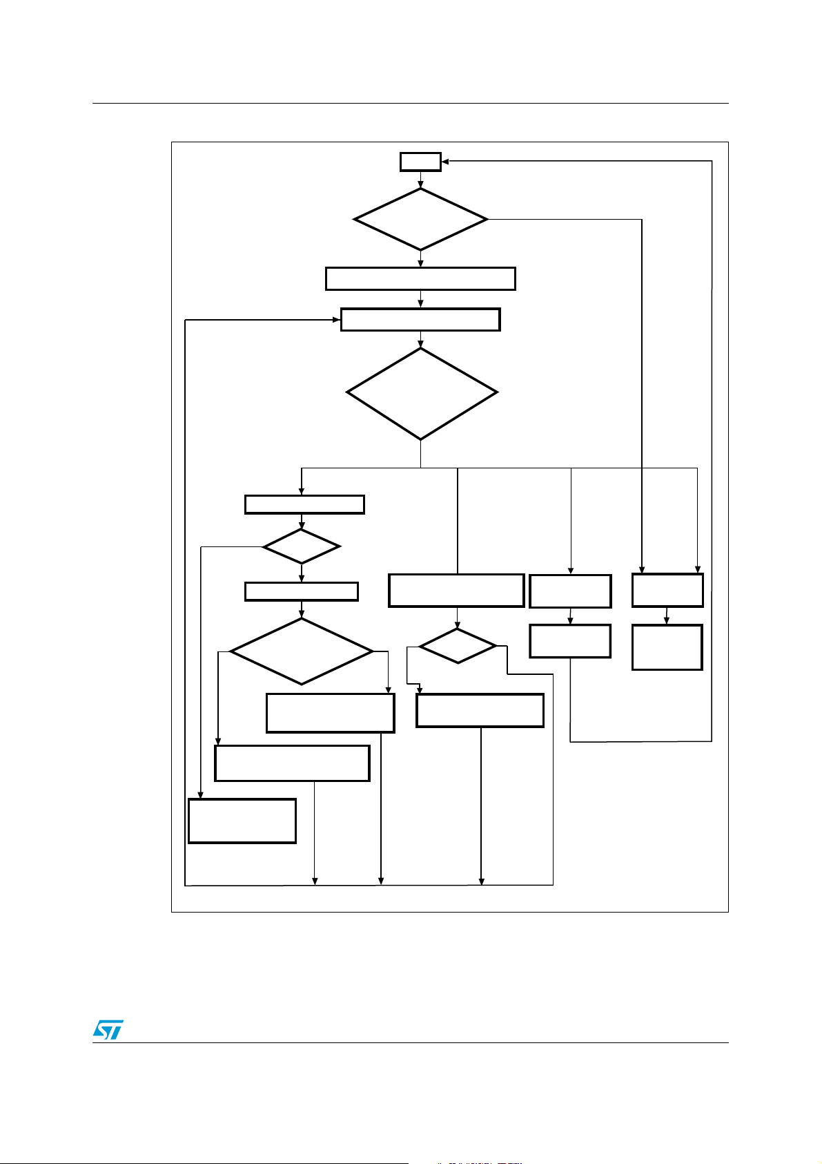
The IAP flowchart is shown in Figure 1: Flowchart of the IAP driver.
4/19 Doc ID 18201 Rev 2
AN3310 IAP overview
No
Yes
Download
Receive a binary file
Success
Yes
Program the Flash
Launch option
byte loading
All data programmed
successfully?
No
Display the name
and size of
Yes
Display the error message
"Verification failed"
Display the error
message "Failed to
receive the file"
Initialize USART
Push-button
is pressed?
Start
Display the IAP main menu
MS19702V1
No
Switch to
user
Switch to
user program
User
application
software
Disable the
write protection
Flash
protection
Upload
Transmit image
of the device internal Flash
Success
Display the error message
"Error occured..."
received file
No
Yes
program
Download, upload,
switch or disable
write-protection
Figure 1. Flowchart of the IAP driver
Doc ID 18201 Rev 2 5/19

Running the IAP driver AN3310
2 Running the IAP driver
For ultra low power medium-density and medium-density plus devices, the IAP driver is
programmed in the Flash memory from Page 0 to Page 47 and the user application
occupies the remaining memory space.
For ultra low power high-density devices, the Flash memory implements the dual bank
feature (Refer to Chapter 9: Dual bank feature for high-density devices).
The IAP driver can be programmed in Bank1 (from Page 0 to Page 47) and the user
application occupies the rest of Flash memory or Bank2.
The IAP driver can be programmed in Bank2 (from Page 768 to Page 814) and the user
application occupies the rest of Bank2 or Bank1.
2.1 HyperTerminal configuration
To use the IAP, the user must have a PC running HyperTerminal or other Terminal program
that supports ymodem protocol. In this document, the HyperTerminal is used. The
following figure shows the HyperTerminal configuration.
Figure 2. COM port properties
Note: The baud rate value of 115,200 bps is used as an example.
Care must be taken when selecting the system clock frequency. To guarantee successful
communication via the USART, the system clock frequency in the end application must be
such that a baud rate equal to 115,200 bps can be generated.
6/19 Doc ID 18201 Rev 2

AN3310 Running the IAP driver
2.2 Executing the IAP driver
As an example in this application note, pressing the pin connected to the push-button allows
the IAP driver to run.
By pressing the push-button at reset, the user can run the IAP driver to reprogram the
STM32L1xx’s internal Flash memory. It is not mandatory to use the push-button; the user
can apply a signal to this pin with respect to its active level. Refer to Table 1: STM32L1xx
IAP implementation.
Doc ID 18201 Rev 2 7/19

IAP driver menu AN3310
3 IAP driver menu
Running the IAP displays the following menu in the HyperTerminal window.
Figure 3. IAP Driver menu when the STM32L1xx Flash memory is not protected
3.1 Downloading an image to the internal Flash memory
To download a binary file via HyperTerminal to the STM32L1xx’s internal Flash memory, do
as follows:
1. Press 1 on the keyboard to select the Download Image To the STM32L1xx Internal
Flash menu
2. Select Send File in the Transfer menu
3. In the Filename field, type the name and the path of the binary file you want to
download
4. From the protocol list, select the Ymodem protocol
5. Click on the Send button
As a result, the IAP driver loads the binary file into the STM32L1xx’s internal Flash memory
from the defined base address and displays the binary file name and size in the
HyperTerminal window.
8/19 Doc ID 18201 Rev 2

AN3310 IAP driver menu
3.2 Uploading an image from the internal Flash memory
To upload a copy of the internal Flash memory started from the user application address, do
as follows:
1. Press 2 on the keyboard to select Upload image from the STM32L1xx internal Flash
menu.
2. Select Receive File in the Transfer menu.
3. Select the directory to save the binary file.
4. From the protocol list, select the Ymodem protocol.
5. Click on the Receive button.
3.3 Executing the new program
Once the new program has been loaded, press 3 on the keyboard to select the Execute
The New Program menu and execute the code.
3.4 Disabling the write protection
When the IAP starts, it checks the Flash memory pages where the user program is to be
loaded to see if any are write-protected. If it is the case, the menu shown in Figure 4
appears.
Figure 4. IAP Driver menu when the STM32L1xx Flash memory is write-protected
Prior to downloading the new program, the write protection must be disabled. To do so,
press 4 (Disable the write protection) on the keyboard. The write protection is disabled
and a system reset is generated to reload the new option byte values. After resuming from
reset, the menu shown in Figure 3 is displayed if the key push-button is pressed.
Note: In this application, the read protection is not supported, so the user has to verify that the
Flash memory is not read-protected.
Doc ID 18201 Rev 2 9/19

STM32L1xx IAP implementation summary AN3310
4 STM32L1xx IAP implementation summary
Ta bl e 1 provides a summary of the STM32L1xx IAP implementation.
Table 1. STM32L1xx IAP implementation
Firmware
IAP program User application Image upload Push-button USART
Option
(1)
byte
Hardware
Low power medium-density devices (STM32L152-EVAL)
The IAP program is
located at 0x8000000.
The Flash routines
(program/erase) are
executed from the Flash
memory except half-page
program routine which is
executed from internal
SRAM. The size of this
program is about 8
Kbytes and programmed
on page 0 to page 47
The user application
(image to be downloaded
with the IAP) will be
programmed starting
from address 0x8003000
(2)
.
The maximum size of the
image to be loaded is 116
Kbytes (page 48 - page
511)
The image is
uploaded with the
IAP from the
STM32L1xx
Internal Flash. The
maximum size of
the image to be
uploaded is
116 Kbytes
(page 48 page 511)
Push-button
(active level:
-
high): Key pushbutton connected
to pin PA.0
Low power high-density devices (STM32L152D-EVAL)
IAP(Bank1) and User app (rest of Flash)
The IAP program is
located at 0x8000000.
The Flash routines
(program/erase) are
executed from the Flash
memory except half-page
program routine which is
executed from internal
(3)
SRAM
.
The size of this program
is about 8 Kbytes and
programmed on page 0
to page 47
The user application
(image to be downloaded
with the IAP) will be
programmed starting
from address 0x8003000
(2)
.
The maximum size of the
image to be loaded is 376
Kbytes (page 48 - page
1535)
The image is
uploaded with the
IAP from the
STM32L1xx
Internal Flash
(Bank1 and
Bank2). The
maximum size of
the image to be
uploaded is
372 Kbytes
(page 48page 1535)
Set
BFB2
in
order
to boot
from
Bank1
Push-button
(active level:
high): Key pushbutton connected
to pin PA.0
USART2
used
USART1
used
IAP(Bank1) and User app (Bank2)
The image is
The IAP program is
located at 0x8000000.
The Flash routines
(program/erase) are
executed from the Flash
memory.
The size of this program
is about 8 Kbytes and
programmed on page 0
to page 47
The user application
(image to be downloaded
with the IAP) will be
programmed starting
from address 0x8030000
(2)
The maximum size of the
image to be loaded is 192
Kbytes (page 768 page 1535)
uploaded with the
IAP from the
STM32L1xx
Internal Flash
(Bank2). The
maximum size of
the image to be
uploaded is
192 Kbytes
(page 768 -
page 1535)
10/19 Doc ID 18201 Rev 2
Set
BFB2
in
order
to boot
from
Bank1
Push-button
(active level:
high): Key pushbutton connected
to pin PA.0
USART1
used

AN3310 STM32L1xx IAP implementation summary
Table 1. STM32L1xx IAP implementation (continued)
Firmware
IAP program User application Image upload Push-button USART
Option
(1)
byte
Low power high-density devices (STM32L152D-EVAL)
IAP(Bank2) and User app (Bank1)
The image is
The IAP program is
located at 0x8030000.
The Flash routines
(program/erase) are
executed from the Flash
Memory.
The size of this program
is about 8 Kbytes and
programmed on page
768 to page 814
The user application
(image to be downloaded
with the IAP) will be
programmed starting
from address 0x8000000
(2)
.
The maximum size of the
image to be loaded is 192
Kbytes (page 0 to page
767)
uploaded with the
IAP from the
STM32L1xx
Internal Flash
(Bank1). The
maximum size of
the image to be
uploaded is
192 Kbytes
(page 0 to
Reset
BFB2
in
order
to boot
from
Bank2
Push-button
(active level:
high): Key pushbutton connected
to pin PA.0
page 767)
IAP and User app (Bank2)
Hardware
USART1
used
The IAP program is
located at 0x8030000.
The Flash routines
(program/erase) are
executed from the Flash
Memory except half-page
program routine which is
executed from internal
(3)
SRAM
.
The size of this program
is about 8 Kbytes and
programmed on
The user application
(image to be downloaded
with the IAP) will be
programmed starting
from address 0x8033000
(2)
.
The maximum size of the
image to be loaded is 180
Kbytes (page 815 to
page 1535)
page 768 to page 814
1. Refer to Chapter 9: Dual bank feature for high-density devices only for the STM32L15xx Low power high-density devices.
2. The user application location address is defined in the flash_if.h file as “#define APPLICATION_ADDRESS
0x08003000”. To modify it, change the default value to the desired one as described in Table 2: Firmware updates.
3. Refer to Table 2: Firmware updates.
The image is
uploaded with the
IAP from the
STM32L1xx
Internal Flash
(Bank2).
The maximum size
of the image to be
uploaded is
180 Kbytes
(page 815 to
page 1535)
Reset
BFB2
in
order
to boot
from
Bank2
Push-button
(active level:
high): Key pushbutton connected
to pin PA.0
USART1
used
The STM32L1xx IAP package comes with:
● Source files and pre-configured projects for the IAP program (under
Project\STM32L1xx_IAP directory)
● Source files and pre-configured projects that build the application to be loaded into the
Flash memory using the IAP (under Project\STM32L1xx_IAP\binary_template
directory).
The readme.txt file provided within this package describes step by step how to execute this
IAP application.
Doc ID 18201 Rev 2 11/19

User program conditions AN3310
Vector table
User code
Vector table
IAP code
0x800 4000
0x800 3FFF
0x800 0000
MS18906V1
Flash memory
Top Flash memory
address
(1)
5 User program conditions
The user application to be loaded into the Flash memory using IAP should be built with
these configuration settings:
1. Set the program load address at 0x08003000, using your toolchain linker file
2. Relocate the vector table at address 0x08003000, using the “NVIC_SetVectorTable”
function.
An example application program to be loaded with the IAP application is provided with
preconfigured projects.
Figure 5. Flash memory usage
12/19 Doc ID 18201 Rev 2
1. Top Flash memory address is equal to:
0x0801 FFFF for ultra low power medium-density devices,
0x0805 FFFF for ultra low power high-density devices.

AN3310 Firmware updates
6 Firmware updates
Table 2. Firmware updates
Cases Defines to be updated in flash_if.h
IAP(Bank1) and
User application
(Rest of Flash)
IAP(Bank1) and
User application
(Bank2)
IAP(Bank2) and
User application
(Bank1)
IAP and
User application
(Bank2)
#define USER_FLASH_LAST_PAGE_ADDRESS
0x0805FF00
#define APPLICATION_ADDRESS 0x08003000
#define FLASH_START_ADDRESS 0x08000000
#define USER_FLASH_LAST_PAGE_ADDRESS
0x0805FF00
#define APPLICATION_ADDRESS 0x08030000
#define FLASH_START_ADDRESS 0x08000000
#define USER_FLASH_LAST_PAGE_ADDRESS
0x0802FF00
#define USER_FLASH_END_ADDRESS 0x0802FFFF
#define APPLICATION_ADDRESS 0x08000000
#define FLASH_START_ADDRESS 0x08030000
#define USER_FLASH_LAST_PAGE_ADDRESS
0x0805FF00
#define APPLICATION_ADDRESS 0x08033000
#define FLASH_START_ADDRESS 0x08030000
Flash routines (half-page
program) executed from
Internal SRAM
(user code to be programmed
in Bank1 (0x08003000 0x0802FF00))
Flash BANK1
(user code to be programmed
in Bank2 (0x08030000 0x0805FF00))
Flash BANK2
(user code to be programmed
in Bank2 (0x08000000 0x0802FF00))
SRAM
(user code to be programmed
in Bank2 (0x08033000 0x0805FF00))
Doc ID 18201 Rev 2 13/19

How to place FLASH programming functions into internal SRAM/FLASH AN3310
7 How to place FLASH programming functions into
internal SRAM/FLASH
Half-page write is only possible from the SRAM or from Bank1 to Bank2 and vice versa.
Depending on the cases named above, the return value of FLASH_ProgramHalfPage()
function in the stm32l1xx_flash_ramfunc.c file should be updated as described in the table
below.
Table 3. Update to the return value of FLASH_ProgramHalfPage()
IAP(Bank1) and
User application
(Rest of Flash)
__RAM_FUNC FLASH_ProgramHalfPage(uint32_t Address,
uint32_t* pBuffer)
IAP(Bank1) and
User application
(Bank2)
IAP(Bank2) and
User application
(Bank1)
IAP and User
application (Bank2)
FLASH_Status FLASH_ProgramHalfPage(uint32_t Address,
uint32_t* pBuffer)
FLASH_Status FLASH_ProgramHalfPage(uint32_t Address,
uint32_t* pBuffer)
__RAM_FUNC FLASH_ProgramHalfPage(uint32_t Address,
uint32_t* pBuffer)
14/19 Doc ID 18201 Rev 2

AN3310 Memory write protection
8 Memory write protection
The write protection should be disabled to the sector where the user code will be
programmed.
.
Table 4. Memory write protection
IAP(Bank1) and
User application
(Rest of Flash)
IAP(Bank1) and
User application
(Bank2)
IAP(Bank2) and
User application
(Bank1)
IAP and
User application
(Bank2)
Write protection should be disabled (WRP, WRP1 and WRP2) except for the
sectors where the IAP code is programmed.
Write protection should be disabled for BANK2 (some sector from WRP1 and
WRP2).
Write protection should be disabled for BANK1 (WRP and some sectors of
WRP1)
Write protection should be disabled for BANK2 (WRP1 and WRP2) except for
the sectors where the IAP code is programmed.
The WRP register controls the write protection from Sector 0 to Sector 31 (128 Kbytes).
The WRP1 register controls the write protection from Sector 32 to Sector 63 (128 Kbytes).
The WRP2 register controls the write protection from Sector 64 to Sector 95 (128 Kbytes).
Doc ID 18201 Rev 2 15/19

Dual bank feature for high-density devices AN3310
9 Dual bank feature for high-density devices
For STM32L15xx high-density devices (these devices have two Flash memory banks:
Bank1 and Bank2), an additional boot mechanism is available which allows booting from
Bank2 or Bank1 (depending on the BFB2 bit status (bit 19 in the user option bytes @
0x1FFFF800)).
At startup, if BFB2 option bit is reset and the boot pins are in the boot from main Flash
memory configuration, the device boots from Flash memory Bank1 or Bank2, depending on
the activation of the bank.
The active banks are checked in the following order: Bank2, followed by Bank1.The active
bank is identified by the value programmed at the base address of the bank (corresponding
to the initial stack pointer value in the interrupt vector table).
1. When the BFB2 bit is reset, after reset, the device boots from the System memory and
executes the embedded code which implements the dual bank mode:
a) First, the code checks Bank2. If it contains a valid code (see Note below), it jumps
to the application located in Bank2.
b) If the Bank2 code is not valid, it checks Bank1 code. If it is valid (see Note below),
it jumps to the application located in Bank1.
c) If both Bank2 and Bank1 do not contain valid code (see Note below), no jump to
Flash banks is executed.
2. When BFB2 bit is set (default state), the dual bank boot mechanism is not performed.
Note: The code is considered as valid when the first data (at the bank start address, which should
be the stack pointer) points to a valid address into the internal SRAM memory (stack top
address). If the first address points to any other location (out of the internal SRAM), the
code is considered not valid.
For more details, a dual bank Boot mode example (FLASH\Dual_Boot) is provided within the
STM32L15xx Standard Peripheral Library available on www.st.com.
16/19 Doc ID 18201 Rev 2

AN3310 Dual bank feature for high-density devices
To change the BFB2 status, add the following functions to your code:
/* Reset BFB2 bit to enable boot from Flash Bank2 */
FLASH_Unlock();
FLASH_OB_Unlock();
FLASH_ClearFlag(FLASH_FLAG_EOP|FLASH_FLAG_WRPERR |
FLASH_FLAG_PGAERR |
FLASH_FLAG_SIZERR | FLASH_FLAG_OPTVERR | FLASH_FLAG_OPTVERRUSR);
FLASH_OB_UserConfig(OB_IWDG_SW, OB_STOP_NoRST, OB_STDBY_NoRST);
FLASH_OB_BORConfig(OB_BOR_LEVEL1);
/* BFB2 option bit will be reset then a system (SW) reset will be
generated. After startup from reset, the device will boot from
Bank2. */
if (FLASH_OB_BootConfig(OB_BOOT_BANK2) == FLASH_COMPLETE)
{
/* generate System Reset to load the new option byte values */
FLASH_OB_Launch();
}
Doc ID 18201 Rev 2 17/19

Revision history AN3310
10 Revision history
Table 5. Revision history
Date Revision Changes
06-Apr-2011 1 Initial release.
Ultra low power high-density devices introduced in Chapter 1: IAP
overview.
Chapter 2: Running the IAP driver updated.
Table 1: STM32L1xx IAP implementation updated.
27-Jan-2012 2
4 new chapters added:
- Chapter 6: Firmware updates,
- Chapter 7: How to place FLASH programming functions into
internal SRAM/FLASH,
- Chapter 8: Memory write protection,
- Chapter 9: Dual bank feature for high-density devices.
18/19 Doc ID 18201 Rev 2

AN3310
Please Read Carefully:
Information in this document is provided solely in connection with ST products. STMicroelectronics NV and its subsidiaries (“ST”) reserve the
right to make changes, corrections, modifications or improvements, to this document, and the products and services described herein at any
time, without notice.
All ST products are sold pursuant to ST’s terms and conditions of sale.
Purchasers are solely responsible for the choice, selection and use of the ST products and services described herein, and ST assumes no
liability whatsoever relating to the choice, selection or use of the ST products and services described herein.
No license, express or implied, by estoppel or otherwise, to any intellectual property rights is granted under this document. If any part of this
document refers to any third party products or services it shall not be deemed a license grant by ST for the use of such third party products
or services, or any intellectual property contained therein or considered as a warranty covering the use in any manner whatsoever of such
third party products or services or any intellectual property contained therein.
UNLESS OTHERWISE SET FORTH IN ST’S TERMS AND CONDITIONS OF SALE ST DISCLAIMS ANY EXPRESS OR IMPLIED
WARRANTY WITH RESPECT TO THE USE AND/OR SALE OF ST PRODUCTS INCLUDING WITHOUT LIMITATION IMPLIED
WARRANTIES OF MERCHANTABILITY, FITNESS FOR A PARTICULAR PURPOSE (AND THEIR EQUIVALENTS UNDER THE LAWS
OF ANY JURISDICTION), OR INFRINGEMENT OF ANY PATENT, COPYRIGHT OR OTHER INTELLECTUAL PROPERTY RIGHT.
UNLESS EXPRESSLY APPROVED IN WRITING BY TWO AUTHORIZED ST REPRESENTATIVES, ST PRODUCTS ARE NOT
RECOMMENDED, AUTHORIZED OR WARRANTED FOR USE IN MILITARY, AIR CRAFT, SPACE, LIFE SAVING, OR LIFE SUSTAINING
APPLICATIONS, NOR IN PRODUCTS OR SYSTEMS WHERE FAILURE OR MALFUNCTION MAY RESULT IN PERSONAL INJURY,
DEATH, OR SEVERE PROPERTY OR ENVIRONMENTAL DAMAGE. ST PRODUCTS WHICH ARE NOT SPECIFIED AS "AUTOMOTIVE
GRADE" MAY ONLY BE USED IN AUTOMOTIVE APPLICATIONS AT USER’S OWN RISK.
Resale of ST products with provisions different from the statements and/or technical features set forth in this document shall immediately void
any warranty granted by ST for the ST product or service described herein and shall not create or extend in any manner whatsoever, any
liability of ST.
ST and the ST logo are trademarks or registered trademarks of ST in various countries.
Information in this document supersedes and replaces all information previously supplied.
The ST logo is a registered trademark of STMicroelectronics. All other names are the property of their respective owners.
© 2012 STMicroelectronics - All rights reserved
STMicroelectronics group of companies
Australia - Belgium - Brazil - Canada - China - Czech Republic - Finland - France - Germany - Hong Kong - India - Israel - Italy - Japan -
Malaysia - Malta - Morocco - Philippines - Singapore - Spain - Sweden - Switzerland - United Kingdom - United States of America
www.st.com
Doc ID 18201 Rev 2 19/19
 Loading...