

Page 1

AN3302
Application note
Monolithic power management for high definition ODD with
true shutdown, reset, and programmable step-up voltage
Introduction
Blu-ray disc players have grown rapidly in popularity due to the increasing availability of
digital services and high definition digital media content.
This application note describes how to use STODDO1, a complete power management for
BIu-ray disc players, based on high density optical storage devices. It integrates two stepdown converters and one step-up.
The step-down converters are optimized for powering Iow-voltage digital core, up to 0.8 A, in
ODD applications and, generally, to replace a high current linear solution when the power
dissipation may cause an overheating of the application environment.
The step-up provides the needed voltage for supplying the blue laser in mobile applications
where only 5 V is available. The output voltage is programmable, by using S-wire protocol, in
the range of 6.5 V to 14 V, with a current capability of 0.7 A.
Figure 1. Blu-ray disc player power management architecture based on STODD01
BLUE Laser Driver
BLUE Laser Driver
6 to 12 V
6 to 12 V
Reset
DSP
DSP
DRAM
DRAM
Flash
Flash
Motors
Motors
The integrated low R
Reset
1.2 V
1.2 V
3.3 V
3.3 V
5 V
5 V
, for N-channel and P-channel MOSFET switches, contributes to
DSon
Reset IC
Reset IC
Step Down
Step Down
ADJ 700 mA
ADJ 700 mA
Step Down
Step Down
3.3 V 700 mA
3.3 V 700 mA
Motor
Motor
Control IC
Control IC
5 V
5 V
Step Up
Step Up
ADJ 800mA
ADJ 800mA
STODD01
STODD01
5 V
5 V
ATA Connector with
ATA Connector with
AM07854v1
AM07854v1
Power
Power
obtaining high efficiency.
The enable function for the step-up section, and reset function for monitoring the input
voltage, make the device particularly suitable for optical storage applications.
The high switching frequency (1.2 MHz typ.) allows the use of tiny surface-mounted
components. Furthermore, a low output ripple is guaranteed by the current mode PWM
topology and by the use of X7R or X5R and low ESR SMD ceramic capacitors.
The device includes soft-start control, thermal shutdown, and peak current limit, to prevent
damage due to accidental overload.
January 2011 Doc ID 18163 Rev 1 1/13
www.st.com
Page 2

Contents AN3302
Contents
1 Block diagram . . . . . . . . . . . . . . . . . . . . . . . . . . . . . . . . . . . . . . . . . . . . . . 3
2 Recommended PCB Iayout . . . . . . . . . . . . . . . . . . . . . . . . . . . . . . . . . . . 4
2.1 Layout considerations . . . . . . . . . . . . . . . . . . . . . . . . . . . . . . . . . . . . . . . . . 4
2.2 Programming the output voltage . . . . . . . . . . . . . . . . . . . . . . . . . . . . . . . . 5
3 Test results . . . . . . . . . . . . . . . . . . . . . . . . . . . . . . . . . . . . . . . . . . . . . . . . 6
3.1 S-wire protocol . . . . . . . . . . . . . . . . . . . . . . . . . . . . . . . . . . . . . . . . . . . . . . 7
3.2 Inductor selection . . . . . . . . . . . . . . . . . . . . . . . . . . . . . . . . . . . . . . . . . . . . 9
3.3 Input and output capacitor selection . . . . . . . . . . . . . . . . . . . . . . . . . . . . . . 9
4 Revision history . . . . . . . . . . . . . . . . . . . . . . . . . . . . . . . . . . . . . . . . . . . 12
2/13 Doc ID 18163 Rev 1
Page 3
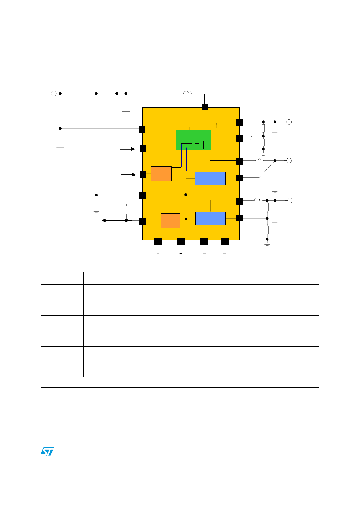
AN3302 Block diagram
1 Block diagram
Figure 2. Block diagram and reference circuit
L1
C1
EN
EN
TX
TX
C1
R5
R5
STODD01
STODD01
V
V
IN_A
IN_A
S-Wire
S-Wire
V
V
IN_P
IN_P
Reset
Reset
Reset
Reset
GND
GND
V
V
IN
IN
C3
C3
C2
C2
Reset
Reset
L1
SW1
SW1
Step Up
Step Up
Step Down
Step Down
Step Down
Step Down
GNDGND
GNDGND
GND
GND
Out1
Out1
FB1
FB1
SW2
SW2
FB2
FB2
SW3
SW3
FB3
FB3
L2
L2
L3
L3
R1
R1
R2
R2
R3
R3
R4
R4
V
V
OUT1
OUT1
C4
C4
6.5V-14V
6.5V-14V
V
V
OUT2
OUT2
3.3V
3.3V
C5
C5
V
V
OUT3
OUT3
0.8V-0.94*Vin
0.8V-0.94*Vin
C6
C6
AM07856v1
AM07856v1
Table 1. List of external components
(1)
Component Manufacturer Part number Value Size
C1, C2, C3 Murata GRM21BR61A1O6KE19L 10 µF 0805
C4, C5, C6 Murata GRM32ER61C226KE2OL 22 µF 1210
L1 Coilcraft LPS6225-472MLB 4.7 µH 6 x 6 x 2.5
L2, L3 Coilcraft LPS4O18-332MLB 3.3 µH 4.1 x 4.1 x 1.8
R1 33 k
R2 3.3 k
R3 27 k
R4 47 k
R5 100 k
Ω (V
Ω (V
= 8.8 V)
OUT1
(2)
Ω 0603
= 1.2 V)
OUT3
(3)
Ω 0603
Ω
(4)
0603
0603
0603
If the S-wire function Is not used, the TX pin must be connected to GND. List of external components
1. Components listed above refer to a typical application. Operation of the STODD01 is not limited to the choice of these
external components.
2. R
and R2 are calculated according to the following formula: R1 = R2 (V
1
It is recommended to use resistors with values in the range of 1 kΩ to 50 kΩ.
and R4 are calculated according to the following formula: R3 = R4 (V
3. R
3
It is recommended to use resistors with values in the range of 1 kΩ to 50 kΩ.
4. It is recommended to use resistors with values in the range of 100 kΩ to 1 MΩ.
OUT1
OUT3
/ V
/ V
FB1
FB3
-1)
-1)
(1)
Doc ID 18163 Rev 1 3/13
Page 4

Recommended PCB Iayout AN3302
2 Recommended PCB Iayout
Figure 3. Recommended PCB layout
2.1 Layout considerations
The layout is an important design step for all switching power supplies due to the high
switching frequency and peak current. If the layout is not performed carefully, important
parameters such as efficiency and output voltage ripple may be out of specification.
Short, wide traces must be implemented for the main current and for power ground paths.
The input capacitor must be placed as close as possible to the IO pins as well as the
inductor and output capacitor.
The feedback pin (FB) connection to the external resistor divider is a high impedance node,
so interference can be minimized by placing the routing of the feedback node as far as
possible from the high current paths. To reduce pick-up noise, the resistor divider must be
placed very close to the device.
A common ground node minimizes ground noise. The exposed pad of the package must be
connected to the common ground node.
AM07857v1AM07857v1
4/13 Doc ID 18163 Rev 1
Page 5

AN3302 Recommended PCB Iayout
2.2 Programming the output voltage
The output voltage for the step-up (ch1) can be adjusted from 6.5 V up to 14 V by
connecting a resistor divider between the V
must be connected to the FB1 pin, as shown in
The resistor divider should be chosen according to the following equation:
Equation 1
and GND, the middle point of the divider
OUT1
Figure 2.
⎞
⎛
R
1
⎟
⎜
VV
+⋅= 1
1FB1OUT
⎟
⎜
R
2
⎠
⎝
where V
is programmable, by using S-wire protocol, in the range of 0.8 V to 1.25 V (see
FB1
Figure 11).
It is recommended to use a resistor with a value in the range of 1 k
Ω to 50 kΩ. Lower values
may also be suitable, but increase current consumption.
For ch2 the device integrates the resistor divider needed to set the correct output voltage
(3.3 V). This allows to save 2 external components. The FB2 pin must be connected directly
to V
OUT2
.
The output voltage for ch3 can be adjusted from 0.8 V up to 94 % of the input voltage value
by connecting a resistor divider between the V
must be connected to the FB3 pin, as shown in
and GND, the middle point of the divider
OUT3
Figure 2.
The resistor divider should be chosen according to the following equation:
Equation 2
⎛
⎞
R
3
⎜
⎟
VV
+⋅= 1
3FB3OUT
⎜
⎟
R
4
⎝
⎠
It is recommended to use a resistor with a value in the range of 1 kΩ to 50 kΩ. Lower values
may also be suitable, but increase current consumption.
Doc ID 18163 Rev 1 5/13
Page 6

Test results AN3302
3 Test results
Figure 4. Inrush current of step-up Figure 5. Enable startup time of step-up
VIN
VIN
VEN
VEN
VOUT
VOUT
STEP-UP
STEP-UP
IIN
IIN
Figure 6. Efficiency ch1 step-up Figure 7. Efficiency ch2-ch3 step-down
VEN
VEN
VOUT1
VOUT1
VOUT2
VOUT2
VOUT3
VOUT3
100
100
90
90
80
80
70
70
60
60
50
50
40
40
30
30
Efficiency [%]
Efficiency [%]
20
20
10
10
0
0
10 100 1000
10 100 1000
Figure 8. Step-down load transient OUT2 Figure 9. Step-down load transient OUT3
V
V
I
I
OUT2
OUT2
V
V
IN_A
IN_A
OUT2
OUT2
= V
= 5 V, VEN= 1.2 V
= V
= 5 V, VEN= 1.2 V
IN_P
IN_P
Step-down
Step-down
Step-down
Step-down
[mA]
[mA]
I
I
OUT
OUT
V
= 7 V
V
= 7 V
OUT
OUT
V
= 9.2 V
V
= 9.2 V
OUT
OUT
100
100
90
90
80
80
70
70
60
60
50
50
40
40
Efficiency [%]
Efficiency [%]
30
30
20
20
10
10
0
0
10 100 1000
10 100 1000
Step-down
Step-down
I
I
OUT3
OUT3
V
Step-down
V
Step-down
OUT3
OUT3
V
= V
V
= V
IN_A
IN_A
I
I
[mA]
[mA]
OUT
OUT
V
V
V
V
= 5 V, VEN= 5 V
= 5 V, VEN= 5 V
IN_P
IN_P
OUT
OUT
OUT
OUT
= 3.3 V
= 3.3 V
= 1.2 V
= 1.2 V
V
V
= V
IN_A
IN_P
= 100-700 mA, C
4.7 µH, L
= 5 V, VEN from 0 to 5 V, V
= L3 = 3.3 µH, T
2
IN1,2,3
= 10 µF, C
= T
rise
fall
OUT2
OUT1,2,3
= 1 µs
= 3.2 V, I
OUT2
= 22 µF, L1 =
= V
IN_A
= 100-700 mA, C
4.7 µH, L
6/13 Doc ID 18163 Rev 1
= 5 V, VEN from 0 to 5 V, V
IN_P
= L3 = 3.3 µH, T
2
IN1,2,3
= 10 µF, C
rise
= T
OUT3
OUT1,2,3
= 1 µs
fall
= 1.2 V, I
OUT3
= 22 µF, L1 =
Page 7

AN3302 Test results
3.1 S-wire protocol
The device implements an S-wire bus communication that uses one control signal coming
from the microprocessor to program the STODD01 output voltage (see
Figure 10. Wire connection
µP
µP
GND
GND
GND
GND
S-wire protocol allows to change the feedback voltage of the step-up section from 0.8 to
1.25 V, with steps of 15 mV. This feature allows complete and easy control of the laser diode
power during read and write operation.
Reset
Reset
EN
EN
TX
TX
Reset
Reset
EN
EN
TX
TX
GND
GND
Figure 10).
STODD01
STODD01
GND
GND
AM07858v1
AM07858v1
If this function isn't used, the TX pin must be connected to GND.
Table 2. Feedback one voltage level
S-wire pulses V
0 (Default Value) 0.800 11 0.965 22 1.130
1 0.815 12 0.980 23 1.145
2 0.830 13 0.995 24 1.160
3 0.845 14 1.010 25 1.175
4 0.860 15 1.025 26 1.190
5 0.875 16 1.040 27 1.205
6 0.890 17 1.055 28 1.220
7 0.905 18 1.070 29 1.235
8 0.920 19 1.085 30 1.250
9 0.935 20 1.100
10 0.950 21 1.115
(V) S-wire pulses V
FB1
(V) S-wire pulses V
FB1
The TX pin must be set to '1' after programming. If TX is programmed with 0 S-wire pulses,
the V
is programmed to 0.8 V.
FB1
FB1
(V)
Doc ID 18163 Rev 1 7/13
Page 8

Test results AN3302
Figure 11. Single wire programming
V
= no change or 0.8 V at startup
V
S-WIRE
S-WIRE
S-WIRE
S-WIRE
S-WIRE
S-WIRE
S-WIRE
S-WIRE
S-WIRE
S-WIRE
S-WIRE
S-WIRE
S-WIRE
S-WIRE
S-WIRE
S-WIRE
S-WIRE
S-WIRE
S-WIRE
S-WIRE
S-WIRE
S-WIRE
S-WIRE
S-WIRE
S-WIRE
S-WIRE
1
1
1
1
1
1
1
1
1
1
1
1
1
1
1
1
1
1
1
1
1
1
= no change or 0.8 V at startup
FB1
FB1
V
= 0.8 V
V
= 0.8 V
FB1
FB1
= 0.815 V
= 0.815 V
V
V
FB1
FB1
V
2
2
32
32
32
32
32
32
32
32
32
32
23
23
3
3
2
2
2
2
3
3
432
432
4
4
4
4
4
4
4
4
4
4
4
4
4
4
V
FB1
FB1
5
5
5
5
5
5
5
5
5
5
5
5
5
5
= 0.83 V
= 0.83 V
V
V
6
6
67
67
67
67
67
67
6
6
6
6
= 0.845 V
= 0.845 V
FB1
FB1
V
V
7
7
7
7
= 0.86 V
= 0.86 V
FB1
FB1
V
V
FB1
FB1
8
8
8
8
8
8
8
8
= 0.875 V
= 0.875 V
V
V
= 0.89 V
= 0.89 V
FB1
FB1
V
V
FB1
FB1
9
9
9
9
10
10
9
9
10
10
= 0.905 V
= 0.905 V
= 0.92 V
= 0.92 V
V
V
FB1
FB1
V
V
FB1
FB1
11
11
12
12
= 0.935 V
= 0.935 V
V
V
= 0.95 V
= 0.95 V
FB1
FB1
1 3
1 3
V
28
28
29
29
30
30
V
FB1
FB1
= 1.25 V
= 1.25 V
AM07859v1
AM07859v1
Figure 12. Example of S-wire programming
VEN
VEN
5 PULSES SEQUENCE
5 PULSES SEQUENCE
DEFAULT VALUE
DEFAULT VALUE
VFB1
VFB1
30 PULSES SEQUENCE
30 PULSES SEQUENCE
8/13 Doc ID 18163 Rev 1
Page 9

AN3302 Test results
(
)
(
)
(
)
(
3.2 Inductor selection
The inductor is the key passive component for switching converters. The inductor selection
must take the boundary conditions in which the converter works into consideration; for the
buck, the maximum input voltage, and for the boost, the minimum input voltage. The critical
inductance values are then obtained according to the following formulas:
for the step-down:
Equation 3
VVV
−⋅
OUTMAX_INOUT
IFV
Δ⋅⋅
LSWMAX_IN
VVV
−⋅
MIN_INOUTMIN_IN
IFV
Δ⋅⋅
LSWOUT
and for the step-up:
Equation 4
L
L
MIN
MIN
=
=
where:
F
: switching frequency.
SW
ΔI
= the peak-to-peak inductor ripple current. As a rule of thumb, the peak-to-peak ripple
L
can be set at 20 % - 40 % of the output current for the step-down and can be set at 20 % 40 % of the input current for the step-up.
The peak current of the inductor must be calculated as:
Equation 5
VVV
−⋅
−−
()
8.0II
OUTDOWNSTEPPEAK
+=
OUTMAX_INOUT
LFV2
⋅⋅⋅
SWMAX_IN
Equation 6
⎛
I
⎜
=
UPSTEPPEAK
−−
⎜
V
⋅η
⎝
⎞
IV
⋅
OUTOUT
⎟
+
⎟
MIN_IN
⎠
VVV
−⋅
SWOUT
)
MIN_INOUTMIN_IN
LFV2
⋅⋅⋅
In addition to the inductance value, in order to avoid saturation, the maximum saturation
current of the inductor must be higher than that of the I
PEAK
.
3.3 Input and output capacitor selection
It is recommended to use ceramic capacitors with X5R or X7R dielectric and Iow ESR as
input and output capacitors in order to filter any disturbance present in the input line and to
obtain stable operation. The output capacitor is very important to satisfy the output voltage
ripple requirement.
Doc ID 18163 Rev 1 9/13
Page 10

Test results AN3302
(
The output voltage ripple (V
OUT_RIPPLE
) in continuous mode, for the step-down channel,
must be calculated as:
Equation 7
⎡
ESRIV
+⋅Δ=
⎢
LRIPPLE_OUT
⎣
⎤
1
⎥
FC8
⋅⋅
SWOUT
⎦
where: ΔIL is the ripple current and FSW is the switching frequency.
The output voltage ripple (V
OUT_RIPPLE
) in continuous mode, for the step-up channel, is:
Equation 8
⎡
ESRIV
+⋅=
⎢
OUTRIPPLE_OUT
⎣
VV
−
⎤
)
INOUT
⎥
FCV
⋅⋅
SWOUTOUT
⎦
where FSW is the switching frequency.
The use of ceramic capacitors with voltage ratings in the range higher than 1.5 times the
maximum input or output voltage is recommended.
Figure 13. Inductor with high I
current Figure 14. Inductor with low I
SAT
The inductors with low saturation current dramatically increase the inductor peak current
value; as shown, using an inductor with low saturation current, the inductor current is higher
than 2.4 A. With the LPS6225-472MLB inductor (I
1 A.
current
SAT
= 3 A) the peak current value is about
SAT
10/13 Doc ID 18163 Rev 1
Page 11

AN3302 Test results
p-Up
p-Up
p-Up
]
p-Up
]
Figure 15. Efficiency Figure 16. Inductor peak current
100
100
98
98
96
96
94
94
92
92
90
90
88
88
86
86
84
84
82
82
Efficiency [%]
Efficiency [%]
80
80
78
78
76
76
74
74
72
72
70
70
290 300 310 320 330 340 350 360 370 380 390 400 410
290 300 310 320 330 340 350 360 370 380 390 400 410
STODD01 Step-UP Section
STODD01 Step-UP Section
BOM Comparison on ST Board
BOM Comparison on ST Board
Ste
Ste
Efficiency vs Load Current
Efficiency vs Load Current
L1=4.7µH (LPS6225-472MLB)
L1=4.7µH (LPS6225-472MLB)
C
C
=22µF (GRM32ER61C226KE20L)
=22µF (GRM32ER61C226KE20L)
4
4
L1=4.7µH (low I
L1=4.7µH (low I
C
C
=22µF (LMK212BJ2226MD)
=22µF (LMK212BJ2226MD)
4
4
current)
current)
sat
sat
Load Current [mA]
Load Current [mA]
VCC = 4V
VCC = 4V
VCC =4.5V
VCC =4.5V
VCC = 5V
VCC = 5V
STODD01 Step-UP Section
STODD01 Step-UP Section
BOM Comparison on ST Board
BOM Comparison on ST Board
Ste
Ste
Inductor Curre nt vs Load Current
2600
2600
L1=4.7µH (low I
L1=4.7µH (low I
2400
2400
=22µF (LMK212BJ2226MD)
=22µF (LMK212BJ2226MD)
C
C
2200
2200
4
4
2000
2000
1800
1800
1600
1600
1400
1400
1200
1200
1000
1000
800
800
600
600
Indu ctor P eak C urrent [ mA
Indu ctor P eak C urrent [ mA
L1=4.7µH (LPS6225-472MLB)
L1=4.7µH (LPS6225-472MLB)
400
400
C
C
=22µF (GRM32ER61C226KE20L)
=22µF (GRM32ER61C226KE20L)
4
4
200
200
0
0
290 300 310 320 330 340 350 360 370 380 390 400 410
290 300 310 320 330 340 350 360 370 380 390 400 410
Inductor Curre nt vs Load Current
current )
current )
sat
sat
Load Current [mA]
Load Current [mA]
The resistance RDC and low saturation current of this inductor have a strong impact on
efficiency and output voltage ripple.
Figure 17. Capacitive change vs. voltage C4
GRM32ER61C226KE20L
Figure 18. Impedance/ESR characteristics C4
GRM32ER61C226KE20L
VCC = 4V
VCC = 4V
VCC =4.5V
VCC =4.5V
VCC = 5V
VCC = 5V
Output voltage ripple depends on output capacitor ESR and by increasing the voltage rating
of the capacitor, as suggested by the BOM list, the switching ripple is minimized.
Doc ID 18163 Rev 1 11/13
Page 12

Revision history AN3302
4 Revision history
Table 3. Document revision history
Date Revision Changes
03-Jan-2011 1 Initial release.
12/13 Doc ID 18163 Rev 1
Page 13

AN3302
Please Read Carefully:
Information in this document is provided solely in connection with ST products. STMicroelectronics NV and its subsidiaries (“ST”) reserve the
right to make changes, corrections, modifications or improvements, to this document, and the products and services described herein at any
time, without notice.
All ST products are sold pursuant to ST’s terms and conditions of sale.
Purchasers are solely responsible for the choice, selection and use of the ST products and services described herein, and ST assumes no
liability whatsoever relating to the choice, selection or use of the ST products and services described herein.
No license, express or implied, by estoppel or otherwise, to any intellectual property rights is granted under this document. If any part of this
document refers to any third party products or services it shall not be deemed a license grant by ST for the use of such third party products
or services, or any intellectual property contained therein or considered as a warranty covering the use in any manner whatsoever of such
third party products or services or any intellectual property contained therein.
UNLESS OTHERWISE SET FORTH IN ST’S TERMS AND CONDITIONS OF SALE ST DISCLAIMS ANY EXPRESS OR IMPLIED
WARRANTY WITH RESPECT TO THE USE AND/OR SALE OF ST PRODUCTS INCLUDING WITHOUT LIMITATION IMPLIED
WARRANTIES OF MERCHANTABILITY, FITNESS FOR A PARTICULAR PURPOSE (AND THEIR EQUIVALENTS UNDER THE LAWS
OF ANY JURISDICTION), OR INFRINGEMENT OF ANY PATENT, COPYRIGHT OR OTHER INTELLECTUAL PROPERTY RIGHT.
UNLESS EXPRESSLY APPROVED IN WRITING BY AN AUTHORIZED ST REPRESENTATIVE, ST PRODUCTS ARE NOT
RECOMMENDED, AUTHORIZED OR WARRANTED FOR USE IN MILITARY, AIR CRAFT, SPACE, LIFE SAVING, OR LIFE SUSTAINING
APPLICATIONS, NOR IN PRODUCTS OR SYSTEMS WHERE FAILURE OR MALFUNCTION MAY RESULT IN PERSONAL INJURY,
DEATH, OR SEVERE PROPERTY OR ENVIRONMENTAL DAMAGE. ST PRODUCTS WHICH ARE NOT SPECIFIED AS "AUTOMOTIVE
GRADE" MAY ONLY BE USED IN AUTOMOTIVE APPLICATIONS AT USER’S OWN RISK.
Resale of ST products with provisions different from the statements and/or technical features set forth in this document shall immediately void
any warranty granted by ST for the ST product or service described herein and shall not create or extend in any manner whatsoever, any
liability of ST.
ST and the ST logo are trademarks or registered trademarks of ST in various countries.
Information in this document supersedes and replaces all information previously supplied.
The ST logo is a registered trademark of STMicroelectronics. All other names are the property of their respective owners.
© 2011 STMicroelectronics - All rights reserved
STMicroelectronics group of companies
Australia - Belgium - Brazil - Canada - China - Czech Republic - Finland - France - Germany - Hong Kong - India - Israel - Italy - Japan -
Malaysia - Malta - Morocco - Philippines - Singapore - Spain - Sweden - Switzerland - United Kingdom - United States of America
www.st.com
Doc ID 18163 Rev 1 13/13
 Loading...