

Page 1

AN3301
Application note
S-Touch® STMPE812A: a hardware and software guide
Introduction
The STMPE812A is a 4-wire resistive touchscreen controller with an integrated 4-bit port
expander. The touchscreen controller is designed to be fully autonomous, requiring only
minimal CPU intervention for sampling, filtering and preprocessing operations.
The purpose of this document is to highlight the guidelines and information complementary
to the datasheet that is necessary for a proper operation of the STMPE812A device in
applications.
The first part of the document highlights information on the hardware. This includes external
components/connectivity, power, PCB design and etc.
The second part of the document focuses on information in software in which programming
reference codes are shown. This part is to be used in conjunction with the STMPE812A
software library available in www.st.com.
December 2010 Doc ID 18161 Rev 1 1/35
www.st.com
Page 2

Contents AN3301
Contents
1 Hardware . . . . . . . . . . . . . . . . . . . . . . . . . . . . . . . . . . . . . . . . . . . . . . . . . . 5
1.1 Typical application circuit and external components . . . . . . . . . . . . . . . . . 5
1.2 Power supply . . . . . . . . . . . . . . . . . . . . . . . . . . . . . . . . . . . . . . . . . . . . . . . 6
1.2.1 Power sequence (fail safe) . . . . . . . . . . . . . . . . . . . . . . . . . . . . . . . . . . . . 6
1.3 Power modes transition . . . . . . . . . . . . . . . . . . . . . . . . . . . . . . . . . . . . . . . 7
1.4 Touchscreen tracks . . . . . . . . . . . . . . . . . . . . . . . . . . . . . . . . . . . . . . . . . . 8
1.4.1 Track resistance . . . . . . . . . . . . . . . . . . . . . . . . . . . . . . . . . . . . . . . . . . . . 8
1.5 Noise prevention . . . . . . . . . . . . . . . . . . . . . . . . . . . . . . . . . . . . . . . . . . . . 9
1.6 Noise filtering . . . . . . . . . . . . . . . . . . . . . . . . . . . . . . . . . . . . . . . . . . . . . . . 9
1.7 PWM controller . . . . . . . . . . . . . . . . . . . . . . . . . . . . . . . . . . . . . . . . . . . . . 10
1.8 ADC controller . . . . . . . . . . . . . . . . . . . . . . . . . . . . . . . . . . . . . . . . . . . . . 11
1.9 GPIO output configurations . . . . . . . . . . . . . . . . . . . . . . . . . . . . . . . . . . . 11
1.9.1 Push-pull . . . . . . . . . . . . . . . . . . . . . . . . . . . . . . . . . . . . . . . . . . . . . . . . 11
1.9.2 Open drain . . . . . . . . . . . . . . . . . . . . . . . . . . . . . . . . . . . . . . . . . . . . . . . 12
2 Software . . . . . . . . . . . . . . . . . . . . . . . . . . . . . . . . . . . . . . . . . . . . . . . . . . 13
2.1 Touchscreen controller acquisition modes . . . . . . . . . . . . . . . . . . . . . . . . 13
2.1.1 Data acquisition by internal timer (ACQ_mode “00”) . . . . . . . . . . . . . . . 13
2.1.2 Data acquisition by ACQ command (ACQ_mode “01”) . . . . . . . . . . . . . 14
2.1.3 Data acquisition by host read control (ACQ_mode “10”) . . . . . . . . . . . . 14
2.2 Embedded data valid bit . . . . . . . . . . . . . . . . . . . . . . . . . . . . . . . . . . . . . . 16
2.3 Pen down interrupt mode . . . . . . . . . . . . . . . . . . . . . . . . . . . . . . . . . . . . 16
2.4 TSC_DATA read . . . . . . . . . . . . . . . . . . . . . . . . . . . . . . . . . . . . . . . . . . . . 17
2.5 Touchscreen controller sampling . . . . . . . . . . . . . . . . . . . . . . . . . . . . . . . 17
2.6 Programming guide . . . . . . . . . . . . . . . . . . . . . . . . . . . . . . . . . . . . . . . . . 19
2.6.1 Touchscreen initialization and interrupt handling (pen down mode) . . . 19
2.6.2 Touchscreen initialization and interrupt handling (normal interrupt mode)
23
2.6.3 GPIO initialization and interrupt handling . . . . . . . . . . . . . . . . . . . . . . . 28
2.6.4 ADC initialization and interrupt handling . . . . . . . . . . . . . . . . . . . . . . . . 29
2.6.5 PWM initialization and interrupt handling . . . . . . . . . . . . . . . . . . . . . . . 32
3 Revision history . . . . . . . . . . . . . . . . . . . . . . . . . . . . . . . . . . . . . . . . . . . 34
2/35 Doc ID 18161 Rev 1
Page 3

AN3301 List of figures
List of figures
Figure 1. Typical application schematic . . . . . . . . . . . . . . . . . . . . . . . . . . . . . . . . . . . . . . . . . . . . . . . . 5
Figure 2. Track resistance . . . . . . . . . . . . . . . . . . . . . . . . . . . . . . . . . . . . . . . . . . . . . . . . . . . . . . . . . . 8
Figure 3. Noise prevention . . . . . . . . . . . . . . . . . . . . . . . . . . . . . . . . . . . . . . . . . . . . . . . . . . . . . . . . . . 9
Figure 4. PWM LED driving configurations . . . . . . . . . . . . . . . . . . . . . . . . . . . . . . . . . . . . . . . . . . . . 10
Figure 5. GPIO push-pull configuration . . . . . . . . . . . . . . . . . . . . . . . . . . . . . . . . . . . . . . . . . . . . . . . 11
Figure 6. GPIO open drain configuration (output low) . . . . . . . . . . . . . . . . . . . . . . . . . . . . . . . . . . . . 12
Figure 7. GPIO open drain configuration (output high) . . . . . . . . . . . . . . . . . . . . . . . . . . . . . . . . . . . 12
Figure 8. Data acquisition by internal timer . . . . . . . . . . . . . . . . . . . . . . . . . . . . . . . . . . . . . . . . . . . . 13
Figure 9. Data acquisition by ACQ command . . . . . . . . . . . . . . . . . . . . . . . . . . . . . . . . . . . . . . . . . . 14
Figure 10. Data acquisition by host read command. . . . . . . . . . . . . . . . . . . . . . . . . . . . . . . . . . . . . . . 15
Figure 11. TSC data register . . . . . . . . . . . . . . . . . . . . . . . . . . . . . . . . . . . . . . . . . . . . . . . . . . . . . . . . 16
Figure 12. Touchscreen controller sampling . . . . . . . . . . . . . . . . . . . . . . . . . . . . . . . . . . . . . . . . . . . . 17
Doc ID 18161 Rev 1 3/35
Page 4

List of tables AN3301
List of tables
Table 1. Power modes vs. touchscreen/GPIO/Interrupt/PWM data . . . . . . . . . . . . . . . . . . . . . . . . . . 7
Table 2. Example of sampling time calculation. . . . . . . . . . . . . . . . . . . . . . . . . . . . . . . . . . . . . . . . . 18
Table 3. Document revision history . . . . . . . . . . . . . . . . . . . . . . . . . . . . . . . . . . . . . . . . . . . . . . . . . 34
4/35 Doc ID 18161 Rev 1
Page 5
AN3301 Hardware
1 Hardware
1.1 Typical application circuit and external components
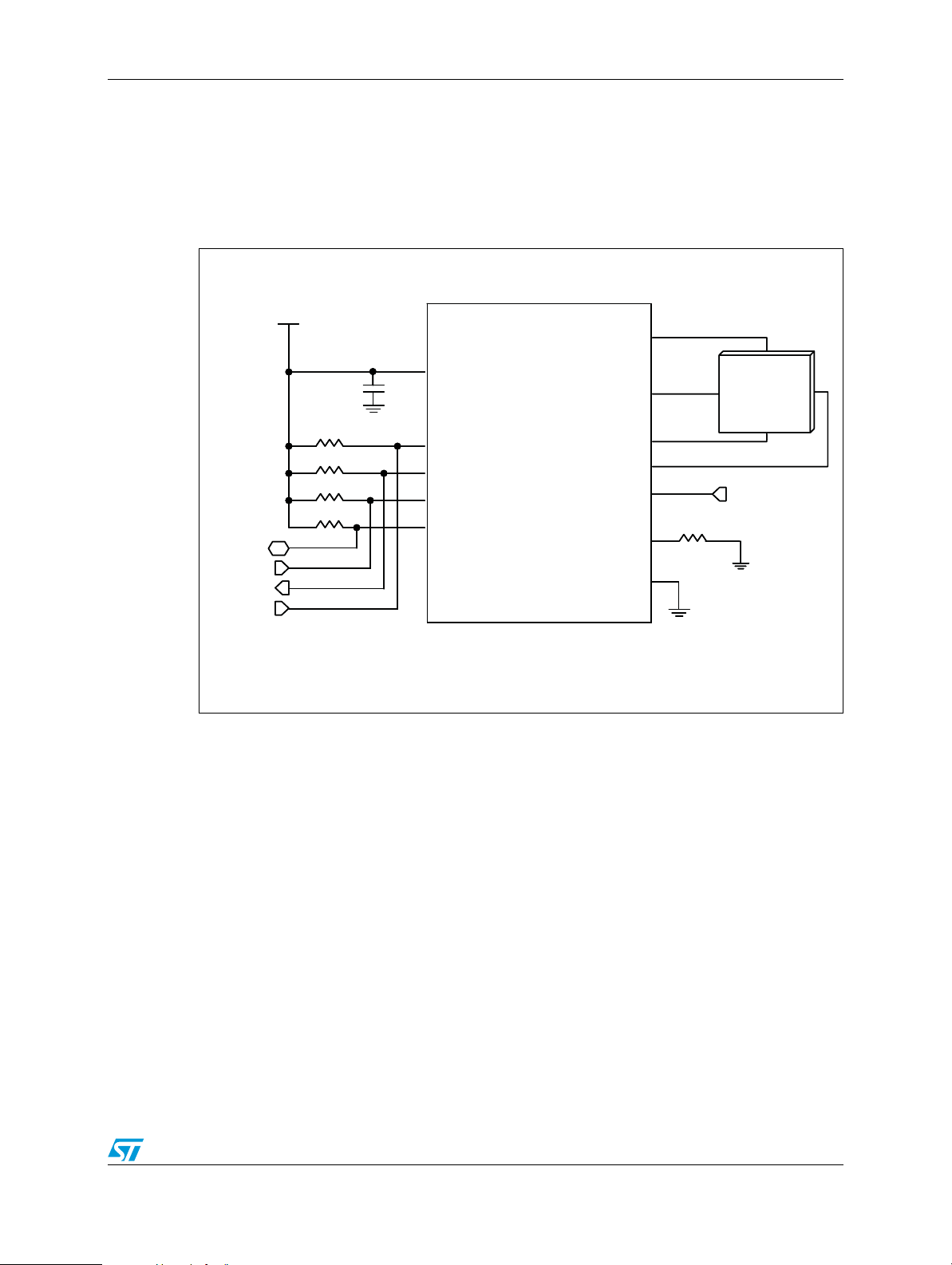
Figure 1. Typical application schematic
1.65V – 3.6V
1.65V – 3.6V
Y+
Y+
VCC
SDA
SDA
SCL
SCL
INT
INT
RESET
RESET
R1
R1
R2
R2
R3
R3
R4
R4
C1
C1
VCC
RESETN
RESETN
INT (P 2)
INT (P 2)
SCLK
SCLK
SDATA
SDATA
STMPE812A
X+
X+
Y-
Y-
X-
X-
(P1)ADC
(P1)ADC
(P0)ADDR
(P0)ADDR
GND
GND
R5
R5
4-wire
resistive
touchscreen
ADC input
ADC input
Note: 1 P0 pin is the I
2 P1 pin is configurable to GPIO/ADC/PWM (ADC Vin must be less than V
3 P2 pin is configurable to GPIO/INT
4 Assuming GPIO controlling RESET input is of open drain type
In a typical application, the following external components are required:
● R1: 2.2k-10kΩ pull up resistor at RESET
● R2: 2.2k-10kΩ pull up resistor at INT.
● R3: 2.2k-10kΩ pull up resistor at SCLK
● R4: 2.2k-10kΩ pull up resistor at SDATA
● R5: 2.2k-10kΩ pull up resistor at ADDR
● C1: 100 nF capacitor at V
2
C address bit upon power up or reset and is configurable to GPIO
)
CC
CC
Doc ID 18161 Rev 1 5/35
AM004192V1
Page 6

Hardware AN3301
1.2 Power supply
The implementation and layout of the power connection’s section is fundamental for the
correct operation of the STMPE812A touchscreen controller.
The STMPE812A device is equipped with a 12-bit ADC that is used during the touchscreen
controller and auxiliary voltage measurement operations.
The analog blocks require a clean and stable supply voltage in order to operate in optimum
performance. In the STMPE812, the analog blocks and the digital core are supplied by V
The operating V
with the increase in V
voltage range is 1.65 V to 3.6 V. Power consumption will be increased
CC
. The lowest power consumption is at VCC = 1.8 V.
CC
It is a good practice to connect a 0.1
pin.
1.2.1 Power sequence (fail safe)
All GPIOs and sense pins of STMPE812A are NOT fail safe. This means that it is necessary
to make sure that the V
inputs.
All other pins (SCL and SDA) are with fail safe structure. It is possible to turn on the pull-up
supply before V
CC
.
supply to STMPE812A is first turned before driving the GPIO
CC
µF filtering capacitor as close as possible to the V
CC
CC
.
6/35 Doc ID 18161 Rev 1
Page 7

AN3301 Hardware
1.3 Power modes transition
The following table highlights the states of touchscreen FIFO, GPIO, Interrupt and PWM
during the various power modes:
– Active mode
– Hibernation mode
– Reset
Table 1. Power modes vs. touchscreen/GPIO/Interrupt/PWM data
Description Active mode Hibernation mode
Touchscreen FIFO data Active Sustained Cleared
GPIO configuration, pin
state and data
Interrupt configuration
and data
PWM configuration and
data
Active Sustained Cleared
Active Sustained Cleared
Active Sustained Cleared
Reset (HW, SW, POR
and General call)
Hibernation mode is entered automatically when ALL of the following listed activities are
met:
● Absent of I
● PWM disabled
● ADC disabled
● Absent of GPIO input transition for 10 ms
● Absent of touchsceen or pen down interrupt for 10 ms
2
C transaction with valid STMPE812A slave address for 10 ms
Doc ID 18161 Rev 1 7/35
Page 8
Hardware AN3301
1.4 Touchscreen tracks
The touchscreen tracks (X+, X-, Y+, Y-) are sensitive lines. Noise may be captured by the
touchscreen tracks if the line is too long and if placed nearby noisy lines, for example the
digital data lines and the I2C/SPI lines.
Although there is no recommended standard for track sizes, tracks that are too long reduce
the resolution of the touchscreen controller. As a matter of fact, long tracks introduce a
voltage drop during the measurement cycle at the terminal of the touchscreen panel.
1.4.1 Track resistance
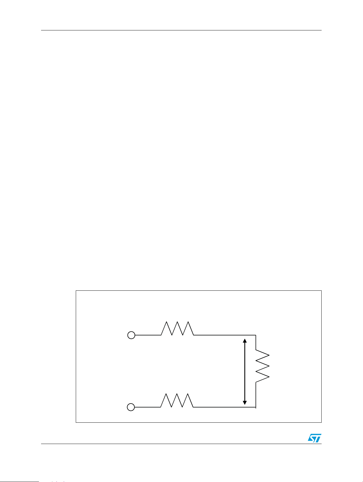
Any track has a certain amount of resistance, thus reducing the effective resolution of the
touchscreen controller.
During the measurement, the current flows to the touchscreen panel through the tracks. If
the resistance is too high, the voltage in the panel terminal is no longer at the same level as
VIO and GND.
From Figure 2 it can be seen that, during the measurement cycle, the device bias the
touchscreen panel with the VIO voltage. Due to the track resistance, the voltage at panel's
terminals is:
Equation 1
Vx V
IO
R
R1 R2 Rx++()⁄⋅=
x
Hence, the effective resolution is reduced by the same factor as well. The track resistance
may be reduced by designing the track as short as possible with a reasonable width.
Figure 2. Track resistance
Tr ack resistance, R1
VIO
To uch panel
Vx
Tr ack resistance, R2
GND
resistance, Rx
8/35 Doc ID 18161 Rev 1
AM004193V2
Page 9
AN3301 Hardware
s
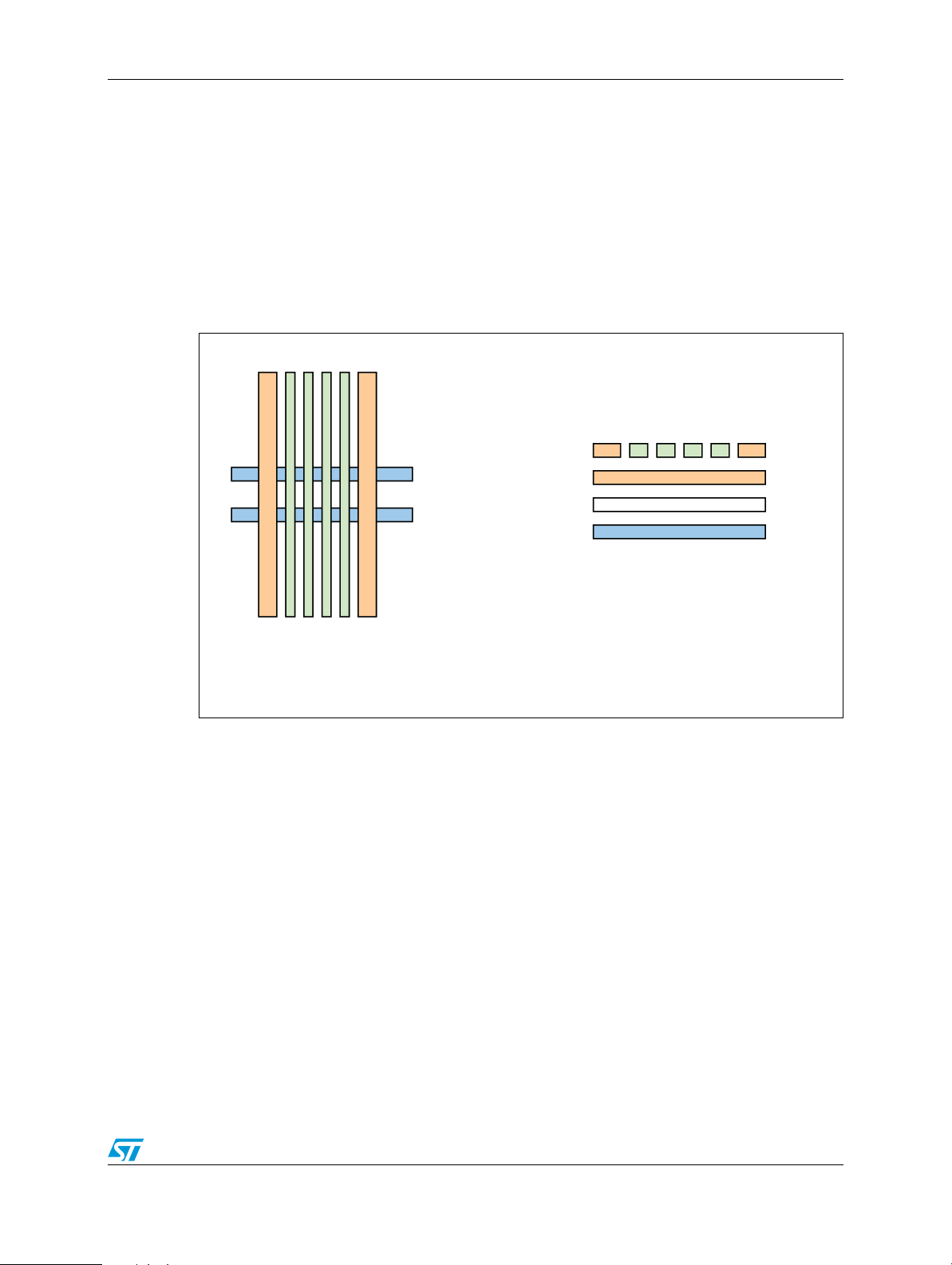
1.5 Noise prevention
Noise may be coupled to the tracks connecting the touchscreen and this should be
prevented as much as possible.
Two practices may be applied:
1. Prevent the tracks overlap with other noisy signal tracks, such as I2C/SPI lines and
digital data lines. If the overlap is not avoidable, GND lines separation between
touchscreen lines and noisy lines is recommended (in more than 2 layers PCB).
2. Put GND shielding at each side of touchscreen tracks routing.
Figure 3. Noise prevention
TSC
TSC tracks
Top Layer
1.6 Noise filtering
A filtering capacitor can be placed on the touchscreen tracks to further suppress the noise.
In this case, the best location for the filtering capacitor is as near as possible to the
STMPE812A sense pins (X+, X-, Y+, Y-).
The values recommended for the filtering capacitor are:
1. 1-2 nF for an LCD less than 6 inches
2. 5-10 nF for an LCD bigger than 6 inches
Noisy tracks
Bottom Layer
GNDGND
GND
Oth er
Noisy lin e
AM004194V2
The Settling time and Touch detect delay registers must be set correctly to adapt to the
filtering capacitor, otherwise the touchscreen controller may not work properly. Additional
information is found in the STMPE812A datasheet.
Doc ID 18161 Rev 1 9/35
Page 10
Hardware AN3301
1.7 PWM controller
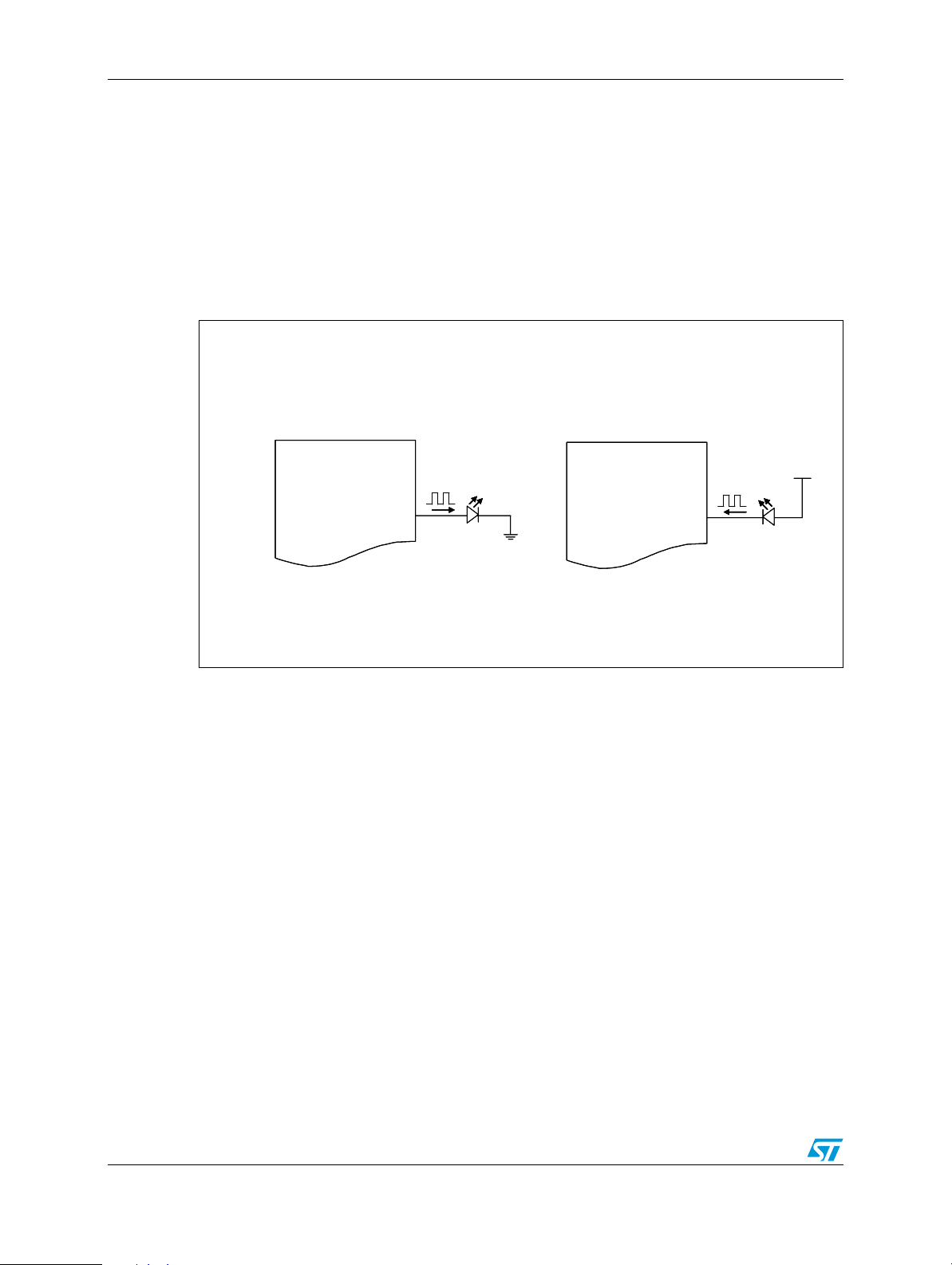
The STMPE812A is integrated with push-pull type of GPIO/PWM outputs. At VCC of 3.3 V,
the outputs are able to provide 8mA of sourcing (out of device) and 12mA of sinking (into
device) current capability. As such, STMPE812A is able to support LED driving in both
sourcing and sinking configuration.
Note: the PWM timing and duty cycle settings in datasheet are based on a LED sourcing
configuration. When used in sinking configuration, the inversion must be executed
accordingly.
Figure 4. PWM LED driving configurations
C u rrent s o urcing
configu ra tion (8 mA)
S TMPE8 12A
S TMPE8 12A
PWM(A1)
PWM(A1)
C u rrent s inking
configu ra tion (12mA)
S TMPE8 12A
S TMPE8 12A
PWM(A1)
PWM(A1)
VCC
VCC
AM004194V1
10/35 Doc ID 18161 Rev 1
Page 11
AN3301 Hardware
1.8 ADC controller
The STMPE812A is equipped with a 12-bit analog-to-digital converter (ADC). Besides the
use for ADC conversion during touchsceen controller operation, it is possible to be used as
general purpose ADC conversion for up to maximum two external auxiliary analog signals
feed through pins B2 and C2.
The touchscreen controller has the priority for the ADC conversion. Selection of conversion
of the two external auxiliary analog signals is programmed through Bit[0] of the ADC control
register (0x20).
Whenever the touchscreen data acquisition is initiated, the ADC conversion is triggered
automatically without needs to program the ADC control register. Writing ‘1’ to Bit[6] of ADC
Control register to initialize conversion for Touchscreen data is redundant and will result in
higher current consumption if ADC is in continuous capture mode.
The STMPE812A is integrated with an internal charge pump in order to ensure ADC
performance in low V
ADC control register in the device initialization phase whenever the V
Important: If V
CC
disabled to prevent possible reliability issue or permanent damage of the device.
condition. The internal charge pump should be turned on through
CC
is less than 2.5 V.
CC
is higher than 2.5 V, it is important to ensure the charge pump is
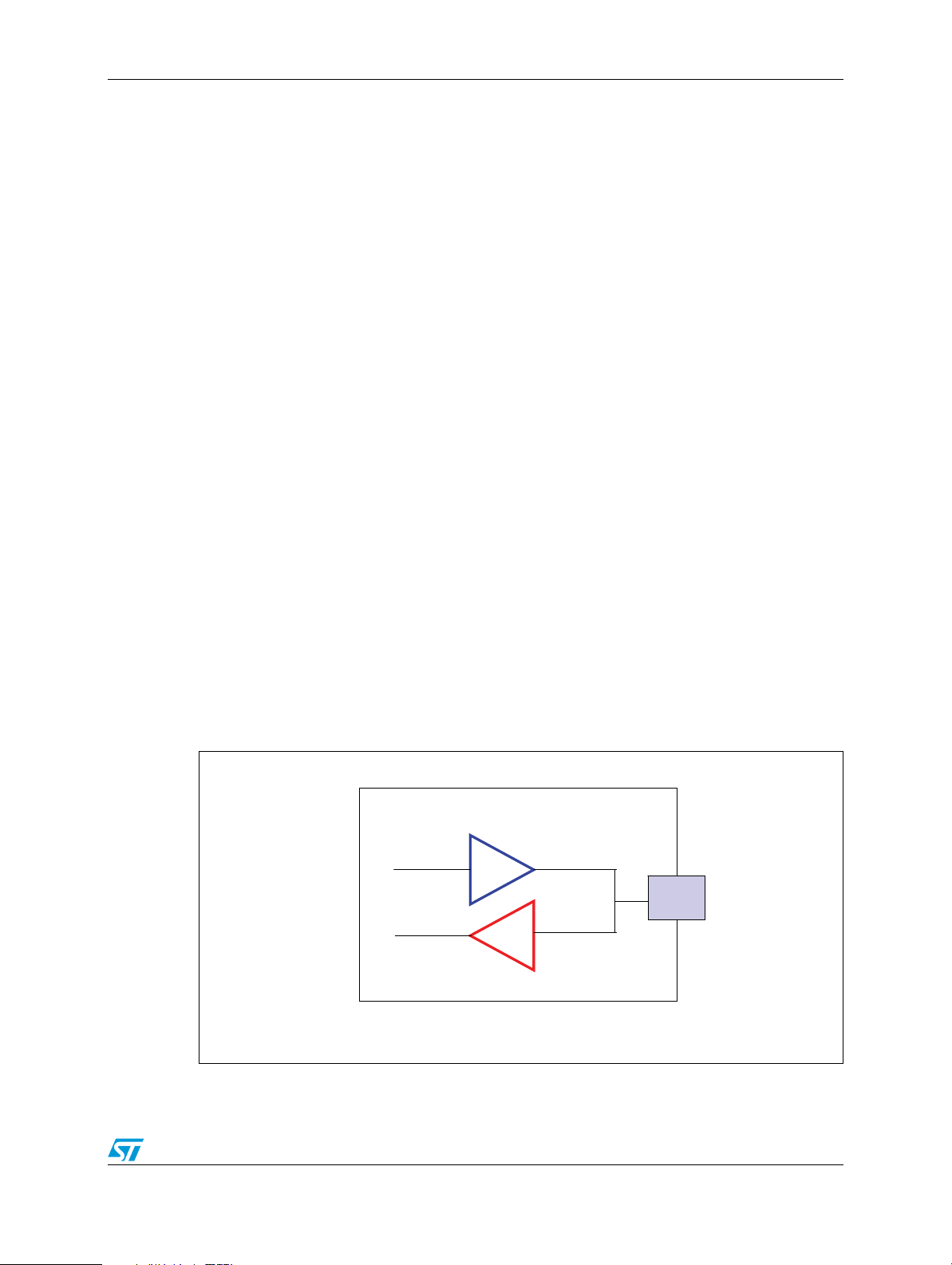
1.9 GPIO output configurations
The STMPE812A provides push-pull type of GPIO output. If open drain GPIO outputs are
required, it is configurable, with a tweak to the software programming routine. See Figure 5,
Figure 6 and Figure 7.
1.9.1 Push-pull
Set the GPIO to output state through PORT_FUNTION (0x04) register. Input path will be
disabled. Output path will be enabled in push-pull configuration.
Figure 5. GPIO push-pull configuration
OUTPUT
INPUT
STMPE812A
disabled
enabled
GPIOxGPIOx
AM004195V1
Doc ID 18161 Rev 1 11/35
Page 12
Hardware AN3301
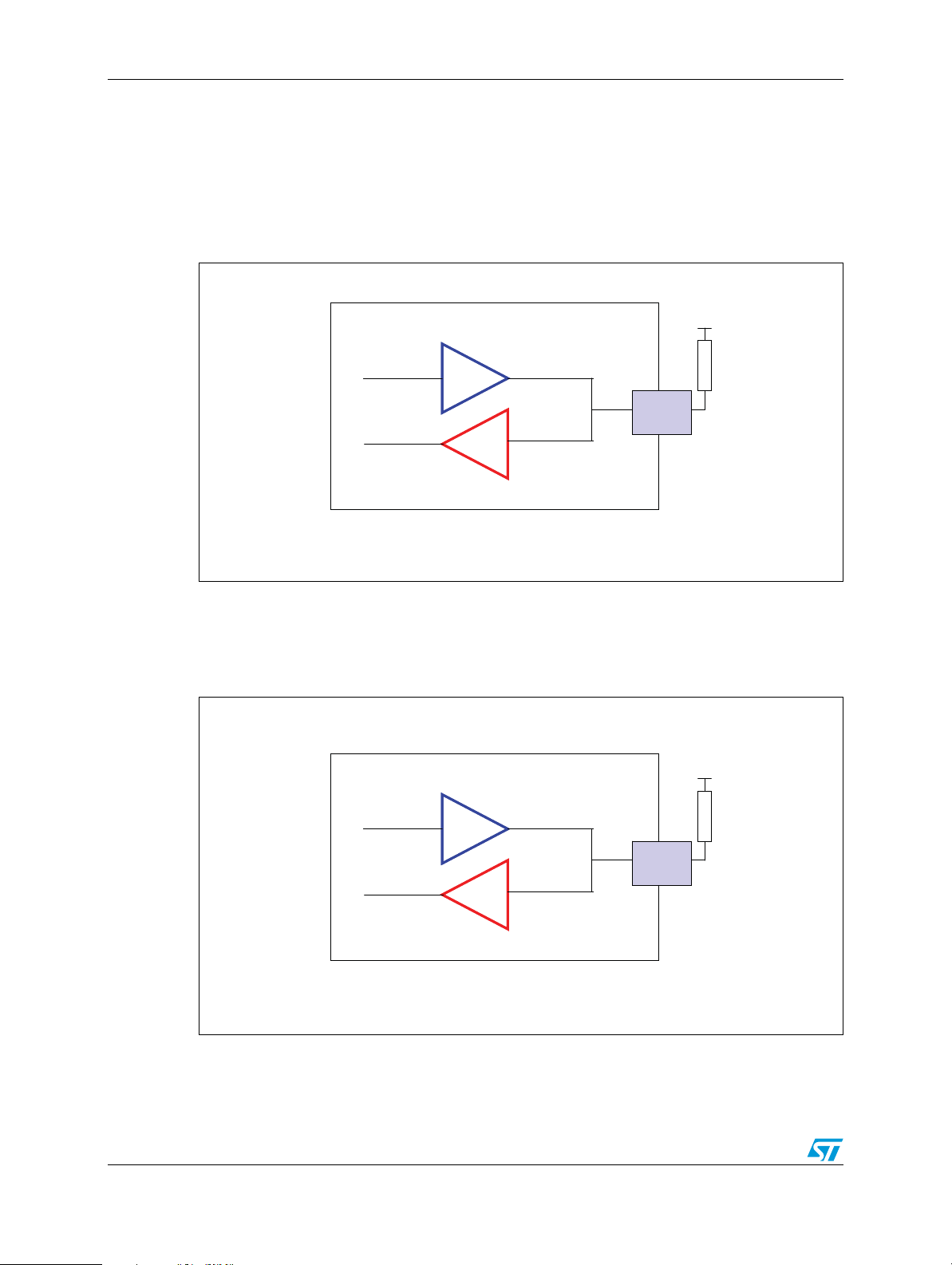
1.9.2 Open drain
GPIO output driven low by STMPE812A
Set the GPIO to output state through PORT_FUNTION (0x04) register. Input path is
disabled. Set the output state to LOW through GPIO_CLR_PIN (0x11) register. Output path
is enabled and pull GPIO pin LOW.
Figure 6. GPIO open drain configuration (output low)
STMPE812A
enable
OUTPUT
GPIOx
INPUT
disable
VCC
External
pull up
GPIOx
GPIO = LOW
AM004197V1
GPIO output pulled high by external pull up resistor
Set the GPIO to input state through PORT_FUNTION (0x04) register. Input path is enabled
and output path disabled. GPIO will be pulled high by external pull up resistor.
Figure 7. GPIO open drain configuration (output high)
STMPE812A
VCC
enable
OUTPUT
INPUT
disable
12/35 Doc ID 18161 Rev 1
GPIOx
GPIOx
GPIO = HIGH
External
pull up
AM004198V1
Page 13

AN3301 Software
2 Software
2.1 Touchscreen controller acquisition modes
2.1.1 Data acquisition by internal timer (ACQ_mode “00”)
In this mode, the system configures STMPE812A to sample at a predefined rate (e.g. 10ms)
through TSC_Sampling_Rate register (0x43). On detecting a touch, it starts the sensing
sequence and on completion of sampling (thus data available for reading), it interrupts the
Host. If the Host does not access the data by the time the next data is available, the old data
is overwritten.
Programming sequence:
1. Initialize touchscreen controller
2. Initialize interrupt
3. Wait for interrupt
4. Upon interrupt, read ISR
5. Upon touch data available, read touch data
Figure 8. Data acquisition by internal timer
Initialization No Touch Touched No Touch
Initializ ation
Agenda:
STMPE812A sens interrupt to Host
Host read ISR
Host read touch data when available
No Touch
Sampling
Sampling
Touched
Sampling
Sampling
Sampling
Sampling
AM004199V1
Doc ID 18161 Rev 1 13/35
Page 14

Software AN3301
2.1.2 Data acquisition by ACQ command (ACQ_mode “01”)
In this acquisition mode, the STMPE812A merely informs the system host on detecting a
touch. As and when sampling is desired, host issues an “ACQ” command that sets
STMPE812A into a complete sampling cycle. Host may read the data after a period of time,
or poll the interrupt status bit for data availability.
Programming sequence:
1. Initialize touchscreen controller
2. Initialize interrupt (Pen Down mode)
3. Wait for interrupt
4. Upon interrupt, issue ACQ command
5. Poll ACQ bit for data available
6. Upon touch data available, read touch data
Figure 9. Data acquisition by ACQ command
Initialization No Touch Touched No Touch
Initializ ation
Agenda:
STMPE812A sens touched interrupt to Host
Host issues ACQ command
Host polls ACQ bit or ISR for sampling completion
Host read touch data when available
No Touch
Sampling
Sampling
Touched
Sampling
Sampling
Sampling
Sampling
2.1.3 Data acquisition by host read control (ACQ_mode “10”)
The data acquisition by the host read control is the most bandwidth efficient method for
touchscreen interfaces. For 100 Hz sampling with 12-bit X, 12-bit Y, 8-bit Z, only one I
transaction (5 bytes data read) is required for every 10 ms. Inclusive of overheads, this
translates to approximately 100 bit time.
At 400 kHz I
A new sample is taken every time the host reads the previously sampled data. If host reads
the data late, the device simply stays longer in hibernation.
2
C speed, this is just 2.5% of total bandwidth.
AM004200V1
2
C
Note: It is necessary to counter check with the data valid bit for each data read.
14/35 Doc ID 18161 Rev 1
Page 15

AN3301 Software
Programming sequence:
1. Initialize touchscreen controller
2. Initialize interrupt (pen down mode)
3. Wait for interrupt
4. Upon interrupt, issue data read (counter check with the embedded data valid bit for the
validity of the corresponding data)
5. Start host timer (typical 10ms depends on the programmed sampling time)
6. Upon time out, issue data read (counter check with the embedded data valid bit for the
validity of the corresponding data)
Figure 10. Data acquisition by host read command
Touched
Initialization
Initialization
No Touch No Touch
No Touch No Touch
Sampling
Sampling
Touched
Sampling
Sampling
Sampling
Sampling
Agenda:
Agenda:
STMPE812 sends touched interrupt to Host
STMPE812 sends touched interrupt to Host
Host read touch data
Host read touch data
Doc ID 18161 Rev 1 15/35
Page 16

Software AN3301
2.2 Embedded data valid bit
In order to facilitate a more bandwidth efficient for data read, it is possible to program
through Bit[5] of TSC_DET_CFG2 register (0x42) whereby the data valid bit is embedded in
within the first byte of the touch data (FIFO).
Figure 11. TSC data register
TSC_DET_CFG2 Register
TSC_DET_CFG2 Register
Bit[4]
Bit[4]
OpMode
OpMode
Bit[5]
Bit[5]
StatusRead
StatusRead
Number of
Number of
bytes to
bytes to
read from
read from
TSC_Data
TSC_Data
510
510
411
411
[11:4] of X400
[11:4] of X400
[11:4] of X301
[11:4] of X301
Da ta valid
Da ta valid
status
status
Da ta valid
Da ta valid
status
status
[3:0] of X
[3:0] of X
[11:8] of Y
[11:8] of Y
[3:0] of X
[3:0] of X
[11:8] of Y
[11:8] of Y
[11:4] of X
[11:4] of X
[11:4] of X
[11:4] of X
[3:0] of X
[3:0] of X
[11:8] of Y
[11:8] of Y
[3:0] of X
[3:0] of X
[11:8] of Y
[11:8] of Y
[7:0] of Y
[7:0] of Y
RSVDVALIDRSVD
RSVDVALIDRSVD
01234567
01234567
Byte4Byte3Byte2Byte1Byte0
Byte4Byte3Byte2Byte1Byte0
-[7:0] o f Z[7:0] of Y
-[7:0] o f Z[7:0] of Y
--[7:0] of Y
--[7:0] of Y
[7:0] of Z[7:0] of Y
[7:0] of Z[7:0] of Y
-
-
AM08680V1
In applications whereby no GPIO input/PWM/ADC is used and Pen Down interrupt mode is
selected, it is no longer necessary to read the ISR register. The data valid info can be
obtained through the embedded data valid bit and the touch release info can be obtained
merely by observing the INT pin signal. (ie. INT low: touched; INT high: release).
2.3 Pen down interrupt mode
In Pen down interrupt mode, the INT pin signal is an OR function of the Pen Down and other
enabled GPIO/PWM/ADC interrupts at Port 0 to Port 3.
It is recommended to use Pen Down mode when the GPIO/PWM/ADC functions are not
required or the GPIO/PWM/ADC interrupts are not enabled. In this condition, the INT signal
provides the exclusive indication for touched (INT low) and release (INT high).
16/35 Doc ID 18161 Rev 1
Page 17

AN3301 Software
2.4 TSC_DATA read
The TSC_DATA contains the converted data for touchscreen controller. Three to five bytes
readings are required depending on the programmed value in TSC_DET_CFG2 register.
In order to preserve the integrity of the data, it is mandatory to ensure the following:
– System host to read exactly the number of bytes according to the programmed
operating mode
2
–I
C host to insert a STOP condition after each data read command
2.5 Touchscreen controller sampling
The touchscreen controller sampling time is determined by the following programmable
parameters:
– Touch detect delay
– Settling time
– ADC conversion time
– MAV (median average filter)
– TSC operating mode (X/Y or X/Y/Z acquisition)
Figure 12 illustrates the diagram of a complete sampling cycle. MAV is acting within the
Sampling period of X, Y and Z respectively.
Figure 12. Touchscreen controller sampling
-
-
Settling Time
To uch Detect Delay
Sampling X
A complete sampling cycle
Settling Time
Sampling Y
Settling Time
Sampling Z
To uch Detect Delay
AM08681V2
The overall sampling time/frequency can be calculated with below formulae.
Sampling time in X/Y/Z mode = touch detect delay *2 + (settling time + (ADC conversion
time * MAV)) * 3
Time taken for sampling in X/Y/Z mode = touch detect delay *2 + (settling time + (ADC
conversion time * MAV)) * 2
Doc ID 18161 Rev 1 17/35
Page 18

Software AN3301
Table 2. Example of sampling time calculation
Sampling
ADC
conversion time
50 µs
Touch detect
delay
Settling time MAV
40 µs 40 µs None
50 µs 40 µs 40 µs 10-2
50 µs 640 µs 640 µs 20-4
time/freq
(complete X/Y/Z
sample sets)
40*2 +
3*(40+(50*1))
=350 µs (2.8 K
sample sets/sec)
40*2 + 3*(40+
(50*10))
=1700 µs (588
sample sets/sec)
640*2 + 3*(640+
(50*20))
=6200 µs (161
sample sets/sec)
18/35 Doc ID 18161 Rev 1
Page 19

AN3301 Software
2.6 Programming guide
In this section, the reference software programming code is shared based on the general
application of the STMPE812A. This includes the initialization and interrupt handling
routines for touchscreen controller (in all 3 acquisition modes and both normal and pen
down interrupt modes), GPIO, ADC and PWM.
The reference code is supplemented by the STMPE812A software library.
2.6.1 Touchscreen initialization and interrupt handling (pen down mode)
The following is an example for touchscreen initialization, interrupt servicing routine in pen
down mode, whereby all other interrupt sources (eg. GPIO, PWM and ADC) are not used in
the application.
A: Initialization
void STMPE812A_Initialization (void) {
/*Enabling the Soft Reset in the System Control Register (0x03)*/
STMPE812A_SoftReset ();
/*Enabling the ADC and TSC Clocks in the System Control Register (0x03)*/
STMPE812A_SetClock (STMPE812A_ENABLE, STMPE812A_ADC_CLK|STMPE812A_TSC_CLK);
/*Setting the Port - 2 as a special function in the Port Function Control Register
(0x04)*/
STMPE812A_SetPortFunction (STMPE812A_PORT2, STMPE812A_PORT_FUNC_SPECIAL_FUNC);
/*Setting the MAV_MODE [2:0] as ‘20 remove 4’, Precharge [1:0] as ‘no pre-charge’ and
Current _Limit [1:0] as ‘20mA’ in the TSC Control Register (0x40) respectively*/
STMPE812A_SetTSCController (STMPE812A_TSC_MAV_20_4, STMPE812A_TSC_NO_PRE,
STMPE812A_TSC_Current20M);
/*Setting the PenStrength [1:0] as ‘Most Sensitive (20K Pull-Up)’, TDetDly [2:0] as
‘40us’ and Settling [2:0] as ‘40us’ in the TSC Detection Configuration 1 Register
(0x41) respectively*/
STMPE812A_ConfigureTSC (STMPE812A_TSC_MOST_SEN, STMPE812A_TSC_TDD40,
STMPE812A_TSC_PDST40);
/*Setting the TSC operating mode OpMode [4] as ’12-bit X, 12-bit Y, 8-bit Z
acquisition’ in the TSC Detection Configuration 2 Register (0x42)*/
STMPE812A_SetTSCOpMode (STMPE812A_DISABLE);
/*Enabling the StatusRead [5] in the TSC Detection Configuration 2 Register (0x42)*/
STMPE812A_SetTSCStatusRead (STMPE812A_ENABLE);
/*Setting the Acq_Mode [7:6] as ‘Data acquisition timed by internal timer’ in the TSC
Detection Configuration 2 Register (0x42)*/
STMPE812A_SetTSCAcquisitionMode (STMPE812A_TSC_INTERNAL_TIMER);
/*Setting the Acq_Mode [7:6] as ‘Data acquisition triggered by a write to “ACQ” bit’
in the TSC Detection Configuration 2 Register (0x42)*/
//STMPE812A_SetTSCAcquisitionMode (STMPE812A_TSC_TRI_ACQ);
/*Setting the Acq_Mode [7:6] as ‘Data acquisition using Host-Controlled Sampling Rate
Control’ in the TSC Detection Configuration 2 Register (0x42)*/
//STMPE812A_SetTSCAcquisitionMode (STMPE812A_TSC_HC_SRC);
/*Setting the TSC sampling rate value of ‘0x0A’ in the TSC Sampling Rate Register
(0x43)*/
STMPE812A_SetTSCSamplingRate (0x0A);
Doc ID 18161 Rev 1 19/35
Page 20

Software AN3301
/*Setting the INT_Mode [7] as ‘Pendown Interrupt Mode’ in the Interrupt Control
Register (0x08)*/
STMPE812A_SetInterruptMode(STMPE812A_INT_MODE_PEN_DOWN);
/*Enabling the Global Interrupt in the Interrupt Control Register (0x08)*/
STMPE812A_EnableGlobalInterrupt (TRUE);
/*Enabling the interrupt from the system related source of TSC_TOUCH and TSC_DATA to
the host in the Interrupt Enable Register (0x09)*/
STMPE812A_EnableInterrupt (STMPE812A_INT_TSC_TOUCH|STMPE812A_INT_TSC_DATA, TRUE);
/*Enabling the TSC operation in the System Control Register (0x03)*/
STMPE812A_EnableTouchscreen (TRUE);}
B: Interrupt handling (pen down mode)
Data acquisition timed by internal timer
void IRQHandler (void) {
u8 data [5];
if (GetITStatus (INTERRUPT_LINE)! = RESET)
{
/*Clearing the Interrupt pending bit from the Micro-controller*/
ClearITPendingBit (INTERRUPT_LINE);
/*Checking the Interrupt Pin Status goes low*/
if ((GPIO_INTERRUPT->IDR & GPIO_PIN_INTERRUPT) == 0)
{
/*Start host timer with an interval of 13ms*/
/*Check below for the timer routine*/
TIM_Cmd (TIM2, ENABLE);
}
}
}
Data acquisition triggered by a write to “ACQ” bit
void IRQHandler (void) {
u8 data [5];
if (GetITStatus (INTERRUPT_LINE)! = RESET)
{
/*Clearing the Interrupt pending bit from the Micro-controller*/
ClearITPendingBit (INTERRUPT_LINE);
/*Checking the Interrupt Pin Status goes low*/
if ((GPIO_INTERRUPT->IDR & GPIO_PIN_INTERRUPT) == 0)
{
/*Start host timer with an interval of 0ms*/
/*Check below for the timer routine*/
TIM_Cmd (TIM2, ENABLE);
}
}
}
20/35 Doc ID 18161 Rev 1
Page 21

AN3301 Software
Data acquisition using host-controlled sampling rate control
void IRQHandler (void) {
u8 data [5];
if (GetITStatus (INTERRUPT_LINE)! = RESET)
{
/*Clearing the Interrupt pending bit from the Micro-controller*/
ClearITPendingBit (INTERRUPT_LINE);
/*Checking the Interrupt Pin Status goes low*/
if ((GPIO_INTERRUPT->IDR & GPIO_PIN_INTERRUPT) == 0)
{
/*Reading the Interrupt status register and Dummy data of 4 bytes of x, y & z data
from the register address of 0x44 to 0x48*/
I2C_Read_Data (STMPE812A_SLAVE_ADDR, STMPE812A_TSC_DATA, 5, &data [0]);
/*Start host timer with an interval of 13ms*/
/*Check below for the timer routine*/
TIM_Cmd (TIM2, ENABLE);
}
}
}
Micro-controller timer routine
Data acquisition timed by internal timer or data acquisition using host-controlled sampling
rate control:
void TIM2_IRQHandler (void) {
if (TIM_GetITStatus (TIM2, TIM_IT_CC1) != RESET)
{
/*Clearing the Timer 2 Interrupt pending bit from the Micro-controller*/
TIM_ClearITPendingBit (TIM2, TIM_IT_CC1);
/*Reading the Interrupt status register and 4 bytes of x, y & z data from the
register address of 0x44 to 0x48*/
I2C_Read_Data (STMPE812A_SLAVE_ADDR, STMPE812A_TSC_DATA, 5, &Touch_Data [0]);
Doc ID 18161 Rev 1 21/35
Page 22

Software AN3301
/*Sets the global variable (Is_Pen_Down) to handle the global variables (Touch_Data
[1] to Touch_Data [4] i.e. 4 bytes of x, y & z data coordinates) in the main while
loop*/
Is_Pen_Down = TRUE;
/*Handling Coordinates codes should be here */
/*Checking either the bit 0 or 1 or both (touch bit [or] data bit [or] touch and
data bits) value from Interrupt status register goes high*/
if ((Touch_Data [0] & 0x03) > 0)
{
/*Getting the Captured value from the Micro-controller Timer2 CNT register*/
Capture = TIM2->CNT;
/*Setting the (Captured value+CCR1_VAL) to the Micro-controller Timer2
CCR1 register.*/
TIM_SetCompare1 (TIM2, capture + CCR1_Val);
/*Enabling the Micro-controller Timer2 for 13ms*/
TIM_Cmd (TIM2, ENABLE);
}
else
{
/*Disabling the Micro-controller Timer2*/
TIM_Cmd (TIM2, DISABLE);
/*Resets the global variable (Is_Pen_Down) to clear the point (x, y & z data
coordinates) in the main while loop*/
Is_Pen_Down = FALSE;
}
}}
Data acquisition triggered by a write to “ACQ” bit
void TIM2_IRQHandler (void) {
if (TIM_GetITStatus (TIM2, TIM_IT_CC1) != RESET)
{
/*Clearing the Timer 2 Interrupt pending bit from the Micro-controller*/
TIM_ClearITPendingBit (TIM2, TIM_IT_CC1);
/* Sets the ACQ [4] in the TSC Control Register (0x40) */
STMPE812A_InitiateAcquisition ();
/* Waiting until the ACQ [4] in the TSC Control Register (0x40) goes low */
while (!STMPE812A_IsAcquisitionComplete ())
22/35 Doc ID 18161 Rev 1
Page 23

AN3301 Software
{}
/*Reading the Interrupt status register and 4 bytes of x, y & z data from the
register address of 0x44 to 0x48*/
I2C_Read_Data (STMPE812A_SLAVE_ADDR, STMPE812A_TSC_DATA, 5, &Touch_Data [0]);
/*Sets the global variable (Is_Pen_Down) to handle the global variables (Touch_Data
[1] to Touch_Data [4] i.e. 4 bytes of x, y & z data coordinates)*/
Is_Pen_Down = TRUE;
/*Handling Coordinates codes should be here */
/*Checking either the bit 0 or 1 or both (touch bit [or] data bit [or] touch and
data bits) value from Interrupt status register goes high*/
if ((Touch_Data [0] & 0x03) > 0)
{
/*Getting the Captured value from the Micro-controller Timer2 CNT register*/
Capture = TIM2->CNT;
/*Setting the (Captured value+CCR1_VAL) to the Micro-controller Timer2
CCR1 register.*/
TIM_SetCompare1 (TIM2, capture + CCR1_Val);
/*Enabling the Micro-controller Timer2 for 0ms*/
TIM_Cmd (TIM2, ENABLE);
}
else
{
/*Disabling the Micro-controller Timer2*/
TIM_Cmd (TIM2, DISABLE);
/*Resets the global variable (Is_Pen_Down) to clear the point (x, y & z data
coordinates) in the main while loop*/
Is_Pen_Down = FALSE;
}
}}
2.6.2 Touchscreen initialization and interrupt handling (normal interrupt mode)
The following is an example for device initialization, interrupt servicing routine in normal
interrupt mode.
A: Initialization
void STMPE812A_Initialization (void) {
/*Enabling the Soft Reset in the System Control Register (0x03)*/
STMPE812A_SoftReset ();
/*Enabling the ADC and TSC Clocks in the System Control Register (0x03)*/
STMPE812A_SetClock (STMPE812A_ENABLE, STMPE812A_ADC_CLK|STMPE812A_TSC_CLK);
/*Setting the Port - 2 as a special function in the Port Function Control Register
(0x04)*/
STMPE812A_SetPortFunction (STMPE812A_PORT2, STMPE812A_PORT_FUNC_SPECIAL_FUNC);
/*Setting the MAV_MODE [2:0] as ‘20 remove 4’, Precharge [1:0] as ‘no pre-charge’ and
Current _Limit [1:0] as ‘20mA’ in the TSC Control Register (0x40) respectively*/
Doc ID 18161 Rev 1 23/35
Page 24

Software AN3301
STMPE812A_SetTSCController (STMPE812A_TSC_MAV_20_4, STMPE812A_TSC_NO_PRE,
STMPE812A_TSC_Current20M);
/*Setting the PenStrength [1:0] as ‘Most Sensitive (20K Pull-Up)’, TDetDly [2:0] as
‘40us’ and Settling [2:0] as ‘40us’ in the TSC Detection Configuration 1 Register
(0x41) respectively*/
STMPE812A_ConfigureTSC (STMPE812A_TSC_MOST_SEN, STMPE812A_TSC_TDD40,
STMPE812A_TSC_PDST40);
/*Setting the TSC operating mode OpMode [4] as ’12-bit X, 12-bit Y, 8-bit Z
acquisition’ in the TSC Detection Configuration 2 Register (0x42)*/
STMPE812A_SetTSCOpMode (STMPE812A_DISABLE);
/*Disabling the StatusRead [5] in the TSC Detection Configuration 2 Register (0x42)*/
STMPE812A_SetTSCStatusRead (STMPE812A_DISABLE);
/*Setting the Acq_Mode [7:6] as ‘Data acquisition timed by internal timer’ in the TSC
Detection Configuration 2 Register (0x42)*/
STMPE812A_SetTSCAcquisitionMode (STMPE812A_TSC_INTERNAL_TIMER);
/*Setting the Acq_Mode [7:6] as ‘Data acquisition triggered by a write to “ACQ” bit’
in the TSC Detection Configuration 2 Register (0x42)*/
//STMPE812A_SetTSCAcquisitionMode (STMPE812A_TSC_TRI_ACQ);
/*Setting the Acq_Mode [7:6] as ‘Data acquisition using Host-Controlled Sampling Rate
Control’ in the TSC Detection Configuration 2 Register (0x42)*/
//STMPE812A_SetTSCAcquisitionMode (STMPE812A_TSC_HC_SRC);
/*Setting the TSC sampling rate value of ‘0x0A’ in the TSC Sampling Rate Register
(0x43)*/
STMPE812A_SetTSCSamplingRate (0x0A);
/*Setting the INT_Mode [7] as ‘Normal Interrupt Mode’ in the Interrupt Control
Register (0x08)*/
STMPE812A_SetInterruptMode(STMPE812A_INT_MODE_NORMAL);
/*Setting the INT_Type [1] as ‘Edge Interrupt Type’ in the Interrupt Control Register
(0x08)*/
STMPE812A_SetInterruptType (STMPE812A_INT_TYPE_EDGE);
/*Enabling the Global Interrupt in the Interrupt Control Register (0x08)*/
STMPE812A_EnableGlobalInterrupt (TRUE);
/*Enabling the interrupt from the system related source of TSC_DATA and TSC_RELEASE
to the host in the Interrupt Enable Register (0x09)*/
/*For Acq_Mode [7:6] in the TSC Detection Configuration 2 Register (0x42) is set as
‘Data acquisition timed by internal timer’*/
STMPE812A_EnableInterrupt (STMPE812A_INT_TSC_DATA|STMPE812A_INT_TSC_REL, TRUE);
/*Enabling the interrupt from the system related source of TSC_TOUCH, TSC_DATA and
TSC_RELEASE to the host in the Interrupt Enable Register (0x09)*/
/*For Acq_Mode [7:6] in the TSC Detection Configuration 2 Register (0x42) is set as
either ‘Data acquisition triggered by a write to “ACQ” bit’ (OR) ‘Data acquisition
using Host-Controlled Sampling Rate Control’*/
//STMPE812A_EnableInterrupt
(STMPE812A_INT_TSC_TOUCH|STMPE812A_INT_TSC_DATA|STMPE812A_INT_TSC_REL, TRUE);
/*Enabling the TSC operation in the System Control Register (0x03)*/
STMPE812A_EnableTouchscreen (TRUE);}
24/35 Doc ID 18161 Rev 1
Page 25

AN3301 Software
B: Interrupt handling (normal interrupt mode)
Data acquisition timed by internal timer
void IRQHandler (void) {
if (GetITStatus (INTERRUPT_LINE)! = RESET)
{
/*Clearing the Interrupt pending bit from the Micro-controller*/
ClearITPendingBit (INTERRUPT_LINE);
/*Reading the Interrupt status register*/
STMPE812A_GetInterruptStatus (&Touch_Data [0]);
/*Reading the 4 bytes of x, y & z data from the register address of 0x44 to 0x47*/
I2C_Read_Data (STMPE812A_SLAVE_ADDR, STMPE812A_TSC_DATA, 4, &Touch_Data [1]);
/*Checking the bit 6(release bit) value from Interrupt status register goes low*/
if ((Touch_Data [0] & 0x40) == 0x00)
{
/*Sets the global variable (Is_Pen_Down) to handle the global variables (Touch_Data
[1] to Touch_Data [4] i.e. 4 bytes of x, y & z data coordinates) in the main while
loop*/
Is_Pen_Down = TRUE;
}
/*Handling Coordinates codes should be here */
}
/*Checking the bit 6(release bit) value from Interrupt status register goes
high*/
if ((Touch_Data [0] & 0x40) == 0x40)
{
/*Resets the global variable (Is_Pen_Down) to clear the point (x, y & z data
coordinates) in the main while loop*/
Is_Pen_Down = FALSE;
}
}}
Data acquisition triggered by a write to “ACQ” bit
void IRQHandler (void) {
if (GetITStatus (INTERRUPT_LINE)! = RESET)
{
/*Clearing the Interrupt pending bit from the Micro-controller*/
ClearITPendingBit (INTERRUPT_LINE);
/*Reading the Interrupt status register*/
STMPE812A_GetInterruptStatus (&Touch_Data [0]);
/*Checking either the bit 0 or 1(touch bit or data bit) value from Interrupt status
register goes high*/
Doc ID 18161 Rev 1 25/35
Page 26

Software AN3301
if (((Touch_Data [0] & 0x01) == 0x01) || ((Touch_Data [0] & 0x02) == 0x02))
{
/*Reading the 4 bytes of x, y & z data from the register address of 0x44 to 0x47*/
I2C_Read_Data (STMPE812A_SLAVE_ADDR, STMPE812A_TSC_DATA, 4, &Touch_Data [1]);
/* Sets the ACQ [4] in the TSC Control Register (0x40) */
STMPE812A_InitiateAcquisition ();
/* Waiting until the ACQ [4] in the TSC Control Register (0x40) goes low */
while (!STMPE812A_IsAcquisitionComplete ())
{}
}
/*Checking the bit 1(data bit) value from Interrupt status register goes high*/
if ((Touch_Data [0] & 0x02) == 0x02)
{
/*Sets the global variable (Is_Pen_Down) to handle the global variables (Touch_Data
[1] to Touch_Data [4] i.e. 4 bytes of x, y & z data coordinates) */
Is_Pen_Down = TRUE;
/*Handling Coordinates codes should be here */
}
/*Checking the bit 6 (release bit) value from Interrupt status register goes high*/
if (((Touch_Data [0] & 0x40) == 0x40))
{
/*Resets the global variable (Is_Pen_Down) to clear the point (x, y & z data
coordinates) in the main while loop*/
Is_Pen_Down = FALSE;
}
}}
Data acquisition using host-controlled sampling rate control
void IRQHandler (void) {
if (GetITStatus (INTERRUPT_LINE)! = RESET)
{
/*Clearing the Interrupt pending bit from the Micro-controller*/
ClearITPendingBit (INTERRUPT_LINE);
26/35 Doc ID 18161 Rev 1
Page 27

AN3301 Software
/*Reading the Interrupt status register*/
STMPE812A_GetInterruptStatus (&Touch_Data [0]);
/*Checking either the bit 0 or 1(touch bit or data bit) value from Interrupt status
register goes high*/
if (((Touch_Data [0] & 0x01) == 0x01) || ((Touch_Data [0] & 0x02) == 0x02))
{
/*Reading the 4 bytes of x, y & z data from the register address of 0x44 to 0x47*/
I2C_Read_Data (STMPE812A_SLAVE_ADDR, STMPE812A_TSC_DATA, 4, &Touch_Data [1]);
}
/*Checking the bit 1(data bit) value from Interrupt status register goes high*/
if ((Touch_Data [0] & 0x02) == 0x02)
{
/*Sets the global variable (Is_Pen_Down) to handle the global variables (Touch_Data
[1] to Touch_Data [4] i.e. 4 bytes of x, y & z data coordinates) in the main while
loop*/
Is_Pen_Down = TRUE;
/*Handling Coordinates codes should be here */
}
/*Checking the bit 6 (release bit) value from Interrupt status register goes high*/
if (((Touch_Data [0] & 0x40) == 0x40))
{
/*Resets the global variable (Is_Pen_Down) to clear the point (x, y & z data
coordinates) in the main while loop*/
Is_Pen_Down = FALSE;
}
}}
Doc ID 18161 Rev 1 27/35
Page 28

Software AN3301
2.6.3 GPIO initialization and interrupt handling
The following is an example for GPIO initialization and interrupt servicing routine.
A: Initialization
void STMPE812A_GPIO_Initialization (void) {
/*Enabling the Soft Reset in the System Control Register (0x03)*/
STMPE812A_SoftReset ();
/*Enabling the GPIO Clock in the System Control Register (0x03)*/
STMPE812A_SetClock (STMPE812A_ENABLE, STMPE812A_GPIO_CLK);
/*Setting the Port - 2 as a special function in the Port Function Control Register
(0x04)*/
STMPE812A_SetPortFunction (STMPE812A_PORT2, STMPE812A_PORT_FUNC_SPECIAL_FUNC);
/*Setting the Port - 1 as a GPIO Input in the Port Function Control Register (0x04)*/
STMPE812A_SetPortFunction (STMPE812A_PORT1, STMPE812A_PORT_FUNC_GPIO_IP);
/*Enabling the IO-1 [1] as GPIO Falling Edge Detection in the GPIO Falling Edge
Detection Register (0x14)*/
STMPE812A_EnableGPIOFallingEdgeInterrupt (STMPE812A_IO1, TRUE);
/*Setting the INT_Mode [7] as ‘Normal Interrupt Mode’ in the Interrupt Control
Register (0x08)*/
STMPE812A_SetInterruptMode(STMPE812A_INT_MODE_NORMAL);
/*Setting the INT_Type [1] as ‘Level Interrupt Type’ in the Interrupt Control
Register (0x08)*/
STMPE812A_SetInterruptType (STMPE812A_INT_TYPE_LEVEL);
/*Enabling the Global Interrupt in the Interrupt Control Register (0x08)*/
STMPE812A_EnableGlobalInterrupt (TRUE);
/*Enabling the interrupt from the system related source of P1 to the host in the
Interrupt Enable Register (0x09)*/
STMPE812A_EnableInterrupt (STMPE812A_INT_P1, TRUE);
}
28/35 Doc ID 18161 Rev 1
Page 29

AN3301 Software
B: Interrupt handling
void IRQHandler (void) {
if (GetITStatus (INTERRUPT_LINE)! = RESET)
{
/*Clearing the Interrupt pending bit from the Micro-controller*/
ClearITPendingBit (INTERRUPT_LINE);
/*Checking the Interrupt Pin Status goes low*/
while ((GPIO_INTERRUPT->IDR & GPIO_PIN_INTERRUPT) == 0)
{
/*Reading the Interrupt status register*/
STMPE812A_GetInterruptStatus (&Touch_Data [0]);
/*Checking the bit 3(P1 bit) value from Interrupt status register goes high*/
if ((Touch_Data [0] & 0x08) == 0x08)
{
/*Printing“GPIO Falling Edge is Detected” on the monitor screen*/
printf (“GPIO Falling Edge is Detected”);
}
}
}}
2.6.4 ADC initialization and interrupt handling
The following is an example for ADC initialization and interrupt servicing routine.
A: Initialization
void STMPE812A_ADC_Initialization (void) {
/*Enabling the Soft Reset in the System Control Register (0x03)*/
STMPE812A_SoftReset ();
/*Enabling the ADC and GPIO Clocks in the System Control Register (0x03)*/
STMPE812A_SetClock (STMPE812A_ENABLE, STMPE812A_ADC_CLK|STMPE812A_GPIO_CLK);
/*Setting the Port - 2 as a special function in the Port Function Control Register
(0x04)*/
STMPE812A_SetPortFunction (STMPE812A_PORT2, STMPE812A_PORT_FUNC_SPECIAL_FUNC);
Doc ID 18161 Rev 1 29/35
Page 30

Software AN3301
/*Setting the Port - 1 as an ADC Input in the Port Function Control Register (0x04)*/
STMPE812A_SetPortFunction (STMPE812A_PORT1, STMPE812A_PORT_FUNC_ADC_IP);
/*Setting the ADC_MODE [7] as 'One-shot capture', ADC_FREQ [5:4] as '15Ksamples/sec'
and ADC_PORT in the ADC Control Register (0x20) respectively*/
STMPE812A_SetADC (STMPE812A_ADC_1_SHOT_CAPTURE, STMPE812A_ADC_FREQ_15K,
STMPE812A_ADC_PORT);
/*Setting the INT_Mode [7] as ‘Normal Interrupt Mode’ in the Interrupt Control
Register (0x08)*/
STMPE812A_SetInterruptMode(STMPE812A_INT_MODE_NORMAL);
/*Setting the INT_Type [1] as ‘Level Interrupt Type’ in the Interrupt Control
Register (0x08)*/
STMPE812A_SetInterruptType (STMPE812A_INT_TYPE_LEVEL);
/*Enabling the Global Interrupt in the Interrupt Control Register (0x08)*/
STMPE812A_EnableGlobalInterrupt (TRUE);
/*Enabling the interrupt from the system related source of P1 to the host in the
Interrupt Enable Register (0x09)*/
STMPE812A_EnableInterrupt (STMPE812A_INT_P1, TRUE);
/*Starting the ADC Conversion (Initiate Data Acquisition by setting the bit [6]) in
the ADC Control Register (0x20)*/
STMPE812A_StartADC (TRUE);
}
Interrupt handling
void IRQHandler (void) {
if (GetITStatus (INTERRUPT_LINE)! = RESET)
{
/*Clearing the Interrupt pending bit from the Micro-controller*/
ClearITPendingBit (INTERRUPT_LINE);
/*Checking the Interrupt Pin Status goes low*/
while ((GPIO_INTERRUPT->IDR & GPIO_PIN_INTERRUPT) == 0)
{
/*Reading the Interrupt status register*/
STMPE812A_GetInterruptStatus (&Touch_Data [0]);
30/35 Doc ID 18161 Rev 1
Page 31

AN3301 Software
/*Checking the bit 3(P1 bit) value from Interrupt status register goes high*/
if ((Touch_Data [0] & 0x08) == 0x08)
{
/*Getting the12 bits ADC data from the ADC Data Register (0x21 & 0x22) */
STMPE812A_GetADCData (&adcdata);
/*Printing the received “adcdata” value on the monitor screen*/
printf ("%ld\n\r", adcdata);
/*Starting the ADC Conversion (Initiate Data Acquisition by setting the bit [6]) in
the ADC Control Register (0x20)*/
STMPE812A_StartADC (TRUE);
}
}
}}
Doc ID 18161 Rev 1 31/35
Page 32

Software AN3301
2.6.5 PWM initialization and interrupt handling
The following is an example for PWM initialization and interrupt servicing routine.
A: Initialization
void STMPE812A_PWM_Initialization (void) {
/*Enabling the Soft Reset in the System Control Register (0x03)*/
STMPE812A_SoftReset ();
/*Enabling the PWM and GPIO Clocks in the System Control Register (0x03)*/
STMPE812A_SetClock (STMPE812A_ENABLE, STMPE812A_PWM_CLK|STMPE812A_GPIO_CLK);
/*Setting the Port - 2 as a special function in the Port Function Control Register
(0x04)*/
STMPE812A_SetPortFunction (STMPE812A_PORT2, STMPE812A_PORT_FUNC_SPECIAL_FUNC);
/*Setting the Port - 1 as a special function in the Port Function Control Register
(0x04)*/
STMPE812A_SetPortFunction (STMPE812A_PORT1, STMPE812A_PORT_FUNC_SPECIAL_FUNC);
/*Setting the Burst_Length [1:0] as ‘8mS’ in the PWMClockDiv Register (0x50) */
STMPE812A_SetPWMBurstLengh (STMPE812A_PWM_BURSTLENGTH_8MS);
/*Setting the Div [4:0] value as ‘0’ in the PWMClockDiv Register (0x50)
respectively*/
STMPE812A_SetPWMClockDivider (0);
/*Setting the Brightness [7:4] as ‘Duty Cycle Ratio 8: 8 (50.00%)’, BurstMultiplier
[3:2] value as ‘1’ and Off_State [1] as ‘PWM Output “LOW” when PWM not running’ in
the PWMControl1 Register (0x51) respectively*/
STMPE812A_ConfigurePWM (STMPE812A_PWM_DUTY_CYCLE_50_00, 1,
STMPE812A_PWM_OFF_STATE_HIGH);
/*Setting the INT_Mode [7] as ‘Normal Interrupt Mode’ in the Interrupt Control
Register (0x08)*/
STMPE812A_SetInterruptMode(STMPE812A_INT_MODE_NORMAL);
/*Setting the INT_Type [1] as ‘Level Interrupt Type’ in the Interrupt Control
Register (0x08)*/
STMPE812A_SetInterruptType (STMPE812A_INT_TYPE_LEVEL);
/*Enabling the Global Interrupt in the Interrupt Control Register (0x08)*/
STMPE812A_EnableGlobalInterrupt (TRUE);
32/35 Doc ID 18161 Rev 1
Page 33

AN3301 Software
/*Enabling the interrupt from the system related source of P1 to the host in the
Interrupt Enable Register (0x09)*/
STMPE812A_EnableInterrupt (STMPE812A_INT_P1, TRUE);
/*Enabling the PWM Controller Sequence in the PWMControl1 Register (0x51)*/
STMPE812A_EnablePWM (TRUE);
}
B: Interrupt handling
void IRQHandler (void) {
if (GetITStatus (INTERRUPT_LINE)! = RESET)
{
/*Clearing the Interrupt pending bit from the Micro-controller*/
ClearITPendingBit (INTERRUPT_LINE);
/*Checking the Interrupt Pin Status goes low*/
while ((GPIO_INTERRUPT->IDR & GPIO_PIN_INTERRUPT) == 0)
{
/*Reading the Interrupt status register*/
STMPE812A_GetInterruptStatus (&Touch_Data [0]);
/*Checking the bit 3(P1 bit) value from Interrupt status register goes high*/
if ((Touch_Data [0] & 0x08) == 0x08)
{
/*Enabling the PWM Controller Sequence in the PWMControl1 Register (0x51)*/
STMPE812A_EnablePWM (TRUE);
}
}
}}
Doc ID 18161 Rev 1 33/35
Page 34

Revision history AN3301
3 Revision history
Table 3. Document revision history
Date Revision Changes
14-Dec-2010 1 Initial release.
34/35 Doc ID 18161 Rev 1
Page 35

AN3301
Please Read Carefully:
Information in this document is provided solely in connection with ST products. STMicroelectronics NV and its subsidiaries (“ST”) reserve the
right to make changes, corrections, modifications or improvements, to this document, and the products and services described herein at any
time, without notice.
All ST products are sold pursuant to ST’s terms and conditions of sale.
Purchasers are solely responsible for the choice, selection and use of the ST products and services described herein, and ST assumes no
liability whatsoever relating to the choice, selection or use of the ST products and services described herein.
No license, express or implied, by estoppel or otherwise, to any intellectual property rights is granted under this document. If any part of this
document refers to any third party products or services it shall not be deemed a license grant by ST for the use of such third party products
or services, or any intellectual property contained therein or considered as a warranty covering the use in any manner whatsoever of such
third party products or services or any intellectual property contained therein.
UNLESS OTHERWISE SET FORTH IN ST’S TERMS AND CONDITIONS OF SALE ST DISCLAIMS ANY EXPRESS OR IMPLIED
WARRANTY WITH RESPECT TO THE USE AND/OR SALE OF ST PRODUCTS INCLUDING WITHOUT LIMITATION IMPLIED
WARRANTIES OF MERCHANTABILITY, FITNESS FOR A PARTICULAR PURPOSE (AND THEIR EQUIVALENTS UNDER THE LAWS
OF ANY JURISDICTION), OR INFRINGEMENT OF ANY PATENT, COPYRIGHT OR OTHER INTELLECTUAL PROPERTY RIGHT.
UNLESS EXPRESSLY APPROVED IN WRITING BY AN AUTHORIZED ST REPRESENTATIVE, ST PRODUCTS ARE NOT
RECOMMENDED, AUTHORIZED OR WARRANTED FOR USE IN MILITARY, AIR CRAFT, SPACE, LIFE SAVING, OR LIFE SUSTAINING
APPLICATIONS, NOR IN PRODUCTS OR SYSTEMS WHERE FAILURE OR MALFUNCTION MAY RESULT IN PERSONAL INJURY,
DEATH, OR SEVERE PROPERTY OR ENVIRONMENTAL DAMAGE. ST PRODUCTS WHICH ARE NOT SPECIFIED AS "AUTOMOTIVE
GRADE" MAY ONLY BE USED IN AUTOMOTIVE APPLICATIONS AT USER’S OWN RISK.
Resale of ST products with provisions different from the statements and/or technical features set forth in this document shall immediately void
any warranty granted by ST for the ST product or service described herein and shall not create or extend in any manner whatsoever, any
liability of ST.
ST and the ST logo are trademarks or registered trademarks of ST in various countries.
Information in this document supersedes and replaces all information previously supplied.
The ST logo is a registered trademark of STMicroelectronics. All other names are the property of their respective owners.
© 2010 STMicroelectronics - All rights reserved
STMicroelectronics group of companies
Australia - Belgium - Brazil - Canada - China - Czech Republic - Finland - France - Germany - Hong Kong - India - Israel - Italy - Japan -
Malaysia - Malta - Morocco - Philippines - Singapore - Spain - Sweden - Switzerland - United Kingdom - United States of America
www.st.com
Doc ID 18161 Rev 1 35/35
 Loading...