


AN3276
Application note
ST solution for efficiency improvement in PFC applications,
back current circuit (BC
Introduction
The challenges for modern high efficiency switching power supplies are to minimize power
losses and increase their power density without raising the cost. The goal is to reduce both
power conduction and power switching losses.
Minimization of power conduction losses is difficult to achieve without considerably affecting
the cost and power density, since more material is required (bigger active and passive
components). Unlike the conduction losses, it is easier to reduce the power switching losses
without significantly increasing the power supply cost. There are two main ways to achieve
this improvement:
■ working on the dynamic behavior of the semiconductor technologies
■ working on circuit topologies
Novel diodes using technologies such as SiC and GaN materials significantly reduce the
switching losses. However, their high price makes them not so attractive for applications
such as desktop server power supplies, solar inverters and µinverters.
2
)
The patented circuit [see Section 5: References, 1.], described in this Application note is
based on the soft switching method and meets market expectations since its
efficiency/cost/power, and density/EMI trade-offs are better than high voltage SiC Schottky
diodes.
November 2010 Doc ID 17975 Rev 1 1/22
www.st.com

Contents AN3276
Contents
1 Existing solutions . . . . . . . . . . . . . . . . . . . . . . . . . . . . . . . . . . . . . . . . . . . 3
1.1 Diode switch-on losses . . . . . . . . . . . . . . . . . . . . . . . . . . . . . . . . . . . . . . . . 3
1.2 Soft switch-on method . . . . . . . . . . . . . . . . . . . . . . . . . . . . . . . . . . . . . . . . 4
1.3 Active recovery circuit . . . . . . . . . . . . . . . . . . . . . . . . . . . . . . . . . . . . . . . . 5
1.4 Passive recovery circuit . . . . . . . . . . . . . . . . . . . . . . . . . . . . . . . . . . . . . . . 6
2 The new ST solution - BC2: energy recovery circuit . . . . . . . . . . . . . . . 7
2.1 Concept description . . . . . . . . . . . . . . . . . . . . . . . . . . . . . . . . . . . . . . . . . . 7
2.2 Phase timing description . . . . . . . . . . . . . . . . . . . . . . . . . . . . . . . . . . . . . . 8
2.2.1 Phase before t0 . . . . . . . . . . . . . . . . . . . . . . . . . . . . . . . . . . . . . . . . . . . . 9
2.2.2 Phase t0 to t1 . . . . . . . . . . . . . . . . . . . . . . . . . . . . . . . . . . . . . . . . . . . . . . 9
2.2.3 Phase t1 to t2 . . . . . . . . . . . . . . . . . . . . . . . . . . . . . . . . . . . . . . . . . . . . . 10
2.2.4 Phase t2 to t3 . . . . . . . . . . . . . . . . . . . . . . . . . . . . . . . . . . . . . . . . . . . . . 11
2.2.5 Phase t3 to t4 . . . . . . . . . . . . . . . . . . . . . . . . . . . . . . . . . . . . . . . . . . . . . 11
2.2.6 Phase t
2.3 Electrical voltage stress in BC2 . . . . . . . . . . . . . . . . . . . . . . . . . . . . . . . . 13
to t
4
5 . . . . . . . . . . . . . . . . . . . . . . . . . . . . . . . . . . . . . . . . . . . . . . . . . . . . . . . . . 12
2.4 Calculation of m2 and m1 ratios . . . . . . . . . . . . . . . . . . . . . . . . . . . . . . . . 13
2.5 Calculation of L . . . . . . . . . . . . . . . . . . . . . . . . . . . . . . . . . . . . . . . . . . . . 14
2.6 Range of products . . . . . . . . . . . . . . . . . . . . . . . . . . . . . . . . . . . . . . . . . . 14
3BC
2
design in 450 W PFC . . . . . . . . . . . . . . . . . . . . . . . . . . . . . . . . . . . . 15
3.1 BC2 design . . . . . . . . . . . . . . . . . . . . . . . . . . . . . . . . . . . . . . . . . . . . . . . . 15
2
3.2 BC
typical waveforms . . . . . . . . . . . . . . . . . . . . . . . . . . . . . . . . . . . . . . 15
3.3 Efficiency comparison . . . . . . . . . . . . . . . . . . . . . . . . . . . . . . . . . . . . . . . 16
3.4 Thermal measurement . . . . . . . . . . . . . . . . . . . . . . . . . . . . . . . . . . . . . . . 18
4 Conclusion . . . . . . . . . . . . . . . . . . . . . . . . . . . . . . . . . . . . . . . . . . . . . . . . 19
5 References . . . . . . . . . . . . . . . . . . . . . . . . . . . . . . . . . . . . . . . . . . . . . . . . 20
6 Revision history . . . . . . . . . . . . . . . . . . . . . . . . . . . . . . . . . . . . . . . . . . . 21
2/22 Doc ID 17975 Rev 1

AN3276 Existing solutions
1 Existing solutions
This section describes some existing areas for efficiency improvements in PFC applications.
1.1 Diode switch-on losses
Usually, in mass market applications between 200 W and 2 kW, a power factor corrector
(PFC) working in continuous conduction mode (CCM) is mandatory. To improve the power
converter density, the switching frequency should be increased. Nevertheless, when the
switching frequency increases, power dissipation in the power switch/rectifier commutation
cells leads to the major switching losses in the PFC. The main power losses occur during
turn-on of the power switch due to both the voltage and current crossing area of the
MOSFET and the reverse recovery losses [see Section 5: References, 2.] produced by the
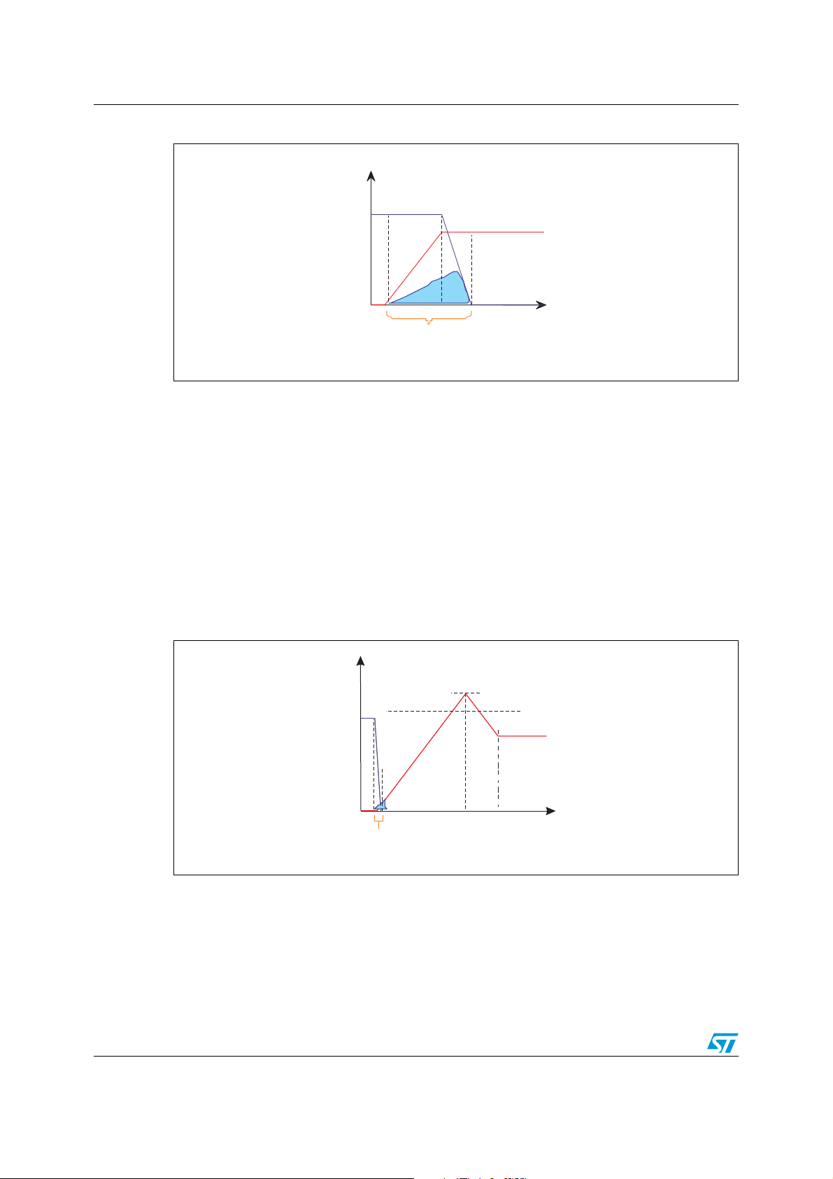
PN diode as shown in Figure 1.
Figure 1. Switch-on losses in PN diode behavior
I+I
V
DS
RM 0
I
0
W
ON
t
Losses are due to area
between I +I and V
0RM DS
To reduce the losses of the PN rectifier, many semiconductor manufacturers have recently
introduced high-voltage Schottky diodes using SiC and GaN technologies. However, it is
impossible to completely remove the voltage and current crossing area during transistor
turn-on by improving component performance only.
Doc ID 17975 Rev 1 3/22
Existing solutions AN3276
Figure 2. Switch-on losses in SiC or GaN diode behavior
V
DS
I
0
t
Losses are due to area
between I and V
0DS
Unlike PN diodes, SiC diodes allow the turn-on dI/dt to be increased without increasing the
diode recovery current. Thus, switching time decreases and switch-on losses decrease too,
but they are not removed entirely. Today, in PFC designs, the turn-on dI/dt with the SiC diode
is around 1000 A/µs maximum to respect EMI standards, whereas the PN diode is used with
a dI/dt of 300 A/µs.
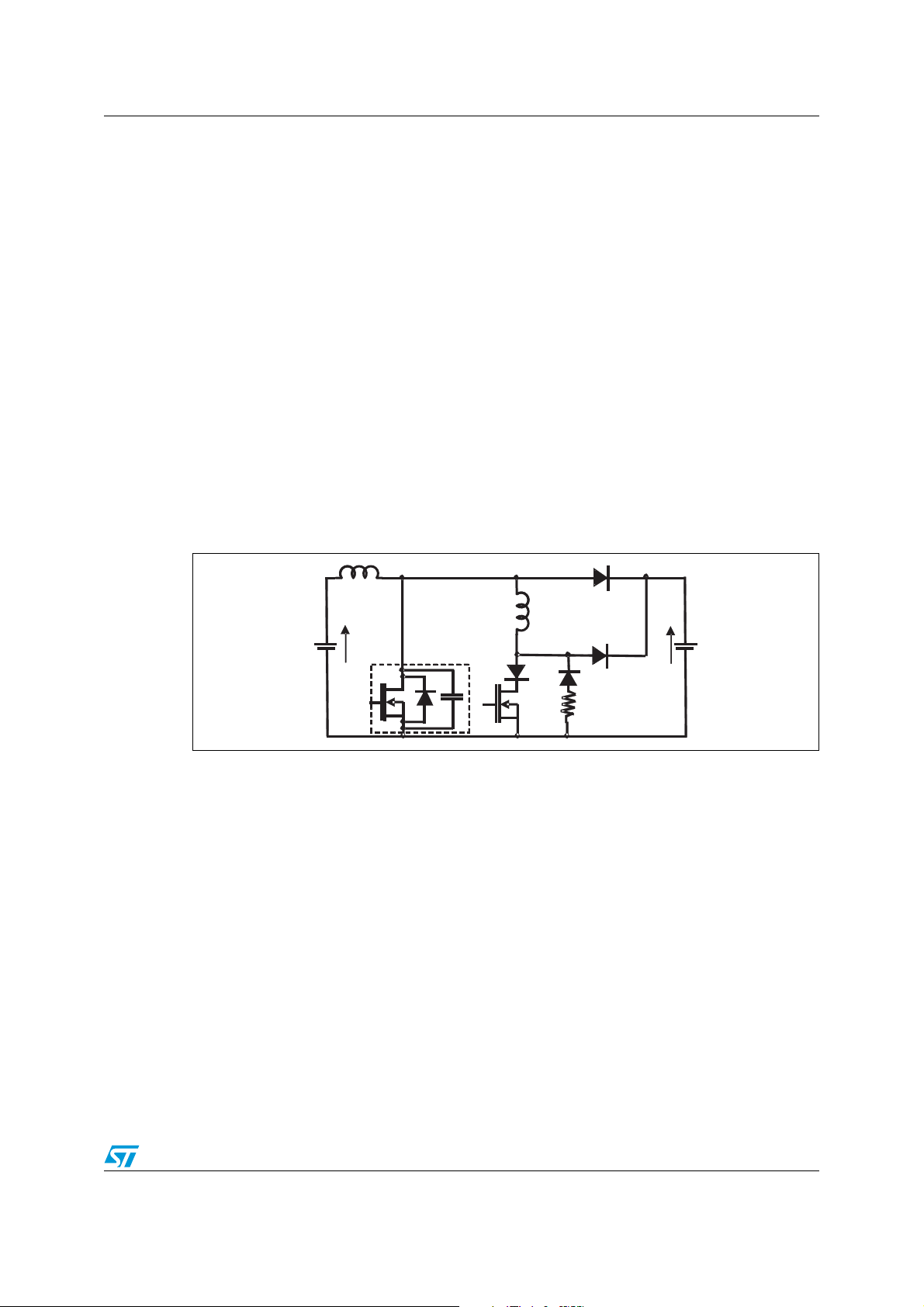
1.2 Soft switch-on method
Another way to reduce these losses is to use a soft switching method by adding a small
inductor L to control the dI/dt slope. This solution removes the current/voltage crossing area
and the PN diode recovery current effect during the turn-on of the transistor as shown in
Figure 3.
Figure 3. Switch-on losses in current soft switching behavior
Small losses:
Zero current switching
V
DS
dI/dt fixed by L
I+I
RM 0
I
0
t
4/22 Doc ID 17975 Rev 1
AN3276 Existing solutions
This soft switching solution is well known, but it requires that several technical criteria be
met:
● Reset the current in the inductor L at each switching period, whatever the variations of
the current, and input and output voltages.
● Recover the saved inductive energy without losses.
● Limit any overvoltage and overcurrent stress in the semiconductor devices.
● Keep cost down when adding any device.
● Maintain a similar power supply density.
There are many circuits that are classified in two families of recovery circuits:
● active
● passive
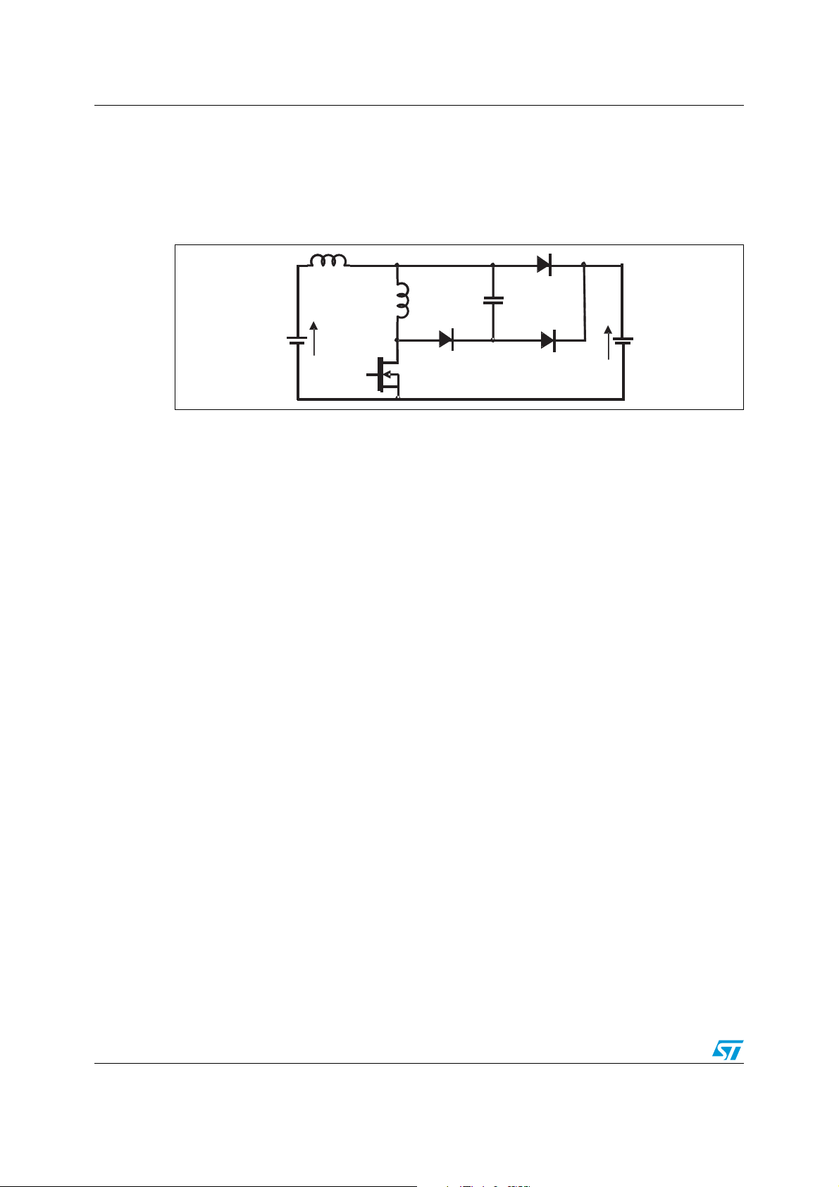
1.3 Active recovery circuit
In the active recovery circuit family, the zero voltage transition (ZVT) [see Section 5:
References, 3.] shown in Figure 4 is well known by designers. This circuit allows both
switch-on and switch-off power losses to be removed.
Figure 4. Zero voltage transition (ZVT) active recovery circuit
L
B
V
mains
L
T
R
D
1
T
ZVT
D
B
D
2
D
damping
R
damping
V
OUT
A theoretical study indicates that ZVT is an excellent topology for the PFC application, since
all the switch losses are removed. In addition, this circuit can work whatever the input and
output power variations. Nevertheless, in practice, the recovery current from the boost diode
D
significantly affects the ZVT behavior leading to some constraints on both inductance
B
and minimum duty cycle. During the reset current in the small inductor L, the recovery
current from D
involves a high-stress voltage and damping parasitic oscillation. Finally, the
2
dynamic behavior of the PN diode affects the global ZVT efficiency because conduction
times in the transistor should increase and a dissipative snubber is mandatory to reduce the
electrical stress across the semiconductors.
In terms of cost the ZVT circuit requires an additional power MOSFET and a specific PWM
controller. Several derivative circuits of the ZVT circuit have the same technical issue and
their higher price makes these circuits less than ideal for mass market applications.
Therefore, the passive recovery circuit can be more attractive.
Doc ID 17975 Rev 1 5/22
Existing solutions AN3276
1.4 Passive recovery circuit
In the passive recovery circuit family the electrical schematic shown in Figure 5 is a good
example [see Section 5: References, 4.]; only two extra diodes and one resonant capacitor
are required.
Figure 5. Passive recovery circuit
L
B
L
V
mains
T
R
This circuit works well under unchanging external conditions. However, it is difficult to design
this kind of system in PFC applications since the current reset in the small inductor depends
on both boost diode recovery current and the external electrical conditions.
Although, the non-dissipative passive circuit requires fewer components, it is unfortunately
technically impractical in PFC applications. These examples highlight that the current
snubber method is well known but the technical challenge is to recover the L energy through
the application without affecting the five criteria listed in Section 1.2.
C
R
D
1
D
B
D
2
V
OUT
6/22 Doc ID 17975 Rev 1
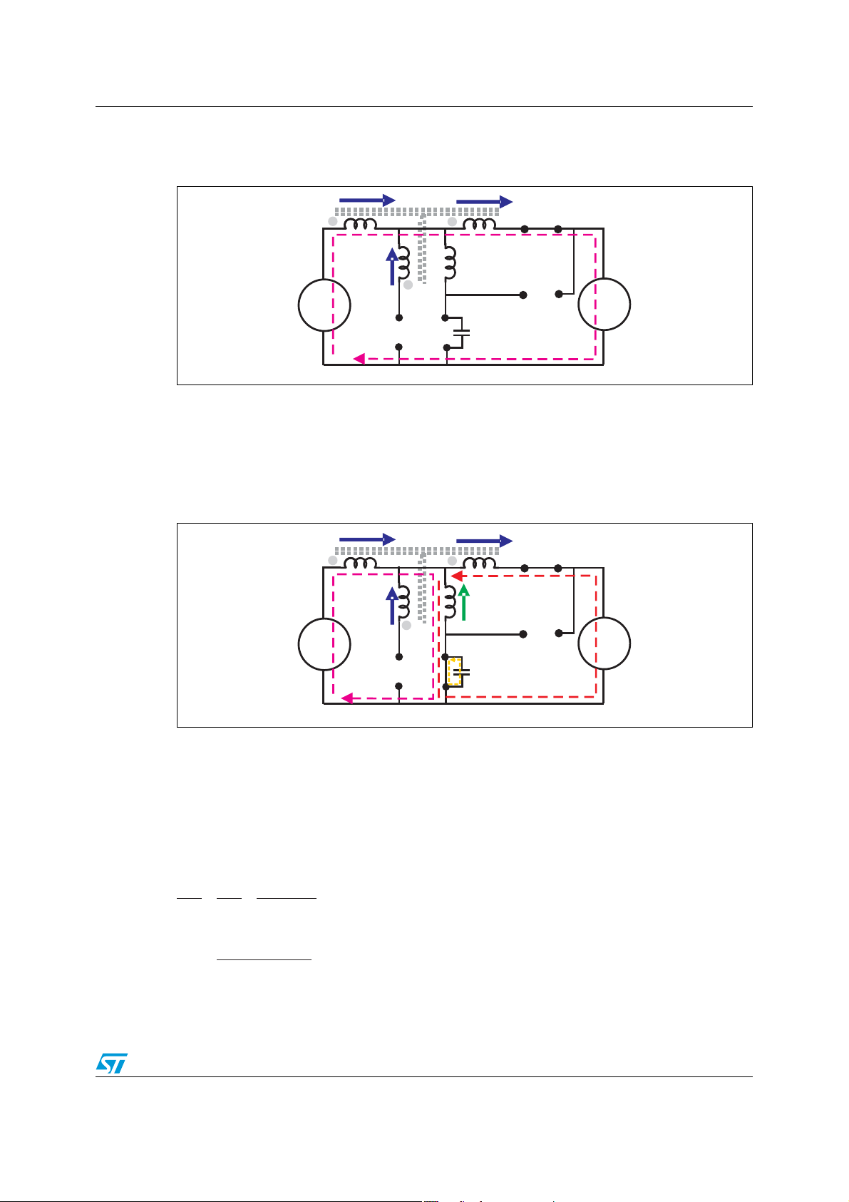
AN3276 The new ST solution - BC2: energy recovery circuit
2 The new ST solution - BC2: energy recovery circuit
The innovative circuit has been designed [see Section 5: References, 1.] to respect the five
soft switching criteria in Section 1.2. Figure 6 shows that two additional diodes D
and two auxiliary windings N
and NS2 wound around the main boost inductor LB are
S1
designed to reset the energy stored in the small inductor L.
and D2
1
Figure 6. Novel energy recovery circuit: BC
L
N
B
p
V
mains
2.1 Concept description
The winding N
boost inductor when the transistor turns on. Since the mains input voltage modulates the L
voltage, it also modulates the reflected voltage across N
modulates the boost diode current I
combined modulations allow the extra current I
the winding N
injected into the output capacitor when the transistor turns off. The reflected voltage across
N
is also a function of the input voltage. This reflected voltage reaches its maximum when
S2
the AC line voltage is low, corresponding to the maximum value of the inductor L current.
These combined variations allow the current flowing in the inductor L to be cancelled in the
bulk capacitor through the diode D
additional windings N
(about 10 A/µs) as in a discontinuous mode switching converter. Their recovery currents do
not affect the behavior of the BC
allows the IRM current from the boost diode DB to be recovered in the main
S1
even in the worst case. The winding NS2 allows the extra current of L to be
S1
and NS2 are to switch off the diodes D1 and D2 with a low dI/dt
S1
2
N
N
S1
D
1
DB
even in the worst case. The benefits of these two
2
2
circuit.
L
T
R
m2=NS2/N
m1=NS1/N
and its associated recovery current IRM. These
flowing in the inductor L to be reset into
RM
D
S2
B
D
2
V
P
P
. This input voltage also
S1
OUT
B
Doc ID 17975 Rev 1 7/22

The new ST solution - BC2: energy recovery circuit AN3276
V
TR
V
L
V
DB
2.2 Phase timing description
Figure 7. Equivalent timing per phase
(IRM+I0)(1+m2)
V
TR
dI
-
=
I
TR
V
L
V
DB
⎛
⎜
I
D2
I
D1
I
DB
⎝
VV
I
0
dI
dt
dt
1
mVV
·+
)m1(
+
2
+
mm
·+-
mainsOUT
-
m1
1
I
·
RM
t
-=
2
2
V
21
D
·+
VmV
·+
2mainsOUT
mains
⎞
⎟
⎠
+
-
1
2
I
1
mainsOUTTR
L)m(
m
1
·)m1(
-
1
I
1
)m1(
2
)m1(
1
·+
VmV
mains2OUTDB
2
·+
L)m1(
V
0UT
-
1 + m
+
t
·
mVV
2
mainOUT
2
-
OUTmains
m1
2
t
)VV(
m
·
2
t
t
t
t
D
2
I
0
t
-I
I
I
mains
The winding ratios m
0
t
0
and m2 versus NP winding are those of the windings NS1 and NS2
1
RM
··2mmmmm
-
-
·
I
RM
t
t
1
2
-
1
1
I
1
I
0
2112
t
t
3
t
4
t
5
respectively.
8/22 Doc ID 17975 Rev 1
AN3276 The new ST solution - BC2: energy recovery circuit
2.2.1 Phase before t
Figure 8. Equivalent circuit before t
Before t0, the BC2 circuit has the same behavior as the conventional boost converter. The
boost diode D
capacitor.
2.2.2 Phase t0 to t
Figure 9. Equivalent circuit t0 to t
conducts to send the main inductor energy through the output bulk
B
1
0
V
mains
0
N
D
S2
I
0
+
-
+
-
N
S
1
D
1
1
I
0
N
S
1
I
0
D
1
L
C
oss
V
L
T
R
C
oss
N
I
S2
RM
D
D
D
V
V
OUT
+
-
OUT
+
-
B
2
B
2
V
mains
At t0, the power MOSFET turns on and the current in DB is equal to I0. At t0+, the current soft
switching occurs, that is to say, the voltage across the power MOSFET decreases to 0 volt
under a zero current and no switching losses appear. After t
increases linearly until it reaches the input current I
whereas the current flowing in D
decreases linearly down to -IRM.
B
added with the recovery diode IRM,
0
Figure 7 shows the behavior of these currents taking account of the m
The simplified dI/dt expression in transistor T
and the boost diode DB can be estimated
R
, the current flowing in L
0
transformer ratio.
2
using,
VV
dI
dI
dt
TRDB
dt
−
N
out
=≈
S2
L
and
V
N
At t
S
=
2
+, the C
0
−
m).VV(
mainsout
2
m1
+
2
capacitance of the power MOSFET is discharged in its R
OSS
DS(on)
. Unlike
standard PFC circuits, the voltage applied across the drain is lower because the reflected
Doc ID 17975 Rev 1 9/22

The new ST solution - BC2: energy recovery circuit AN3276
dI
V
voltage is subtracted from V
NS2
. This behavior provides the BC2 circuit with a benefit
OUT
since under the low output load, power saving occurs in the system and it can be evaluated
using:
2
P
C
OSS
1
t
−
0
2
Thus, the BC
⎡
2
⎢
V.C.
outOSS
⎢
⎣
2
reduces switch-off losses too.
+
⎛
−=
⎜
⎝
mainsout
m1
+
2
⎤
m.VV
⎞
2
⎥
F.
⎟
switching
⎥
⎠
⎦
2.2.3 Phase t1 to t
Figure 10. Equivalent circuit t1 to t2
At t
+, the boost diode DB turns off, and an overcurrent IRM is stored in the small inductor.
1
This overcurrent discharges the D
voltage polarity across the main inductor changes until it reaches D
this time, the overcurrent I
inductor.
Thus, the current flowing through N
L
at the same time as the Np winding biased by the mains voltage. The IRM current flowing
B
in D
decreases down to reach 0 A thanks to the reflected voltage V
1
V
=
1NS
m.V
−
mains
m1
−
1
1
2
V
+
-
mains
C
B
j
D
N
S2
I
0
V
L
N
S
1
I
RM
D
1
T
R
junction capacitance linearly. At the same time, the
B
is reduced by the transformer ratio m1 and is sent to the main
RM
contributes to charge the internal coil magnetization
S1
V
OUT
D
2
+
-
diode conduction. At
1
that it is given by:
NS1
and
)1m1.(L.I
−
RM
_t
≈
ON1D
To guarantee a soft switching behavior in discontinuous mode, the current in D
reach 0 A before time t
current is the largest when the V
addition, to cancel the D
the low reflected voltage V
_
−
D
1
≈
dt
Unfortunately, during this phase a high reverse voltage is applied across the boost diode D
10/22 Doc ID 17975 Rev 1
mains
mains
−
outreverse_DB
m.V
1
should
. The t
3
recovery current diode effect, the dI/dt_D1 is always low thanks to
1
m.V
1
NS1
time trend supports the PFC application since the IRM
D1_ON
voltage in the sinusoidal period is the highest. In
mains
and it is given by:
1
L).1m1(
:
N
S
2
1
S
−
m.(V
mains
VVVVV
+=++=
out
N
)2m
+
1
m1
1
B

AN3276 The new ST solution - BC2: energy recovery circuit
This feature requires a specific diode for this application, so ST has developed an optimized
diode with an accurate trade-off between the I
current value and its breakdown voltage.
RM
2.2.4 Phase t2 to t
Figure 11. Equivalent circuit t2 to t
At t2, the current in D1 reaches 0 A and then the BC2 works as a conventional power boost
converter. As the power transistor stays on, the current in the main L
inductor increases up to I
2.2.5 Phase t3 to t
3
V
4
+
-
mains
I
1
N
at time t3.
1
3
C
B
j
D
N
S2
V
L
S
1
D
1
T
R
D
V
OUT
2
+
-
and the small L
B
Figure 12. Equivalent circuit t3 to t
N
S
V
mains
+
-
4
N
D
S2
I
1
V
L
1
C
D
1
oss
D
V
B
2
OUT
+
-
At t3, the power transistor turns off. At this time the voltage across the MOSFET increases
linearly as its C
reach conduction in diode D
capacitance is charged by the current stored in the small inductor L to
OSS
. No overvoltage stress occurs on the power switch during the
2
turn off. At the same time, the voltage polarity across the main inductor changes until it
reaches D
shared as shown in Figure 7. The current in D
voltage from N
reach the nominal current at t
diode conduction. As soon as the diodes conduct together, the output current is
B
to reach 0 A with a low dI/dt. On the other hand, the current in DB rises to
S2
. This shared current is a benefit for the BC2 circuit. In the
4
starting at I1, decreases due to the reflected
2
PFC application working under a lower mains voltage such as 90 V rms, the highest
Doc ID 17975 Rev 1 11/22

The new ST solution - BC2: energy recovery circuit AN3276
application boost current is shared between DB and D1 diodes. Therefore the conduction
losses in the rectification stage are reduced. The reflected voltage V
and D2 time
NS2
conduction are given by:
V
=
N
2
S
−−
+
m).VV(
mainsout
2
m1
2
and
+−
ON_2D
−
1
=
t
)2m1.(L.I
m).VV(
mainsout
2
The t
V
mains
2
BC
circuit even under the worst case PFC applications such as high output load current
time trend supports the PFC application since the I1 current is largest when the
D2_ON
voltage range is lowest. Thus the discontinuous mode could be guaranteed in the
under the minimum V
diode effect, the dI/dt_D
_dI
D
≈
dt
2.2.6 Phase t4 to t
Figure 13. Equivalent circuit t4 to t
voltage range. In addition, to cancel the D2 recovery current
mains
is always low due to the low reflected voltage V
2
−−
+
m).VV(
mainsout2
2
L).2m1(
given by:
NS2
5
5
V
B
OUT
2
+
-
V
mains
N
D
S2
I
0
+
N
S
1
L
D
D
1
C
oss
At t4, the current in the D2 reaches 0 A and then the BC2 works like a conventional power
boost converter. Only the boost diode D
conducts. Due to the reflected voltage of NS2, the
B
voltage across the power switch is lower than V
in the bulk capacitor and power saving occurs as the transistor turns on at t
12/22 Doc ID 17975 Rev 1
. Thus the C
OUT
capacitor is discharged
OSS
.
0

AN3276 The new ST solution - BC2: energy recovery circuit
2.3 Electrical voltage stress in BC
Ta bl e 1 summarizes the maximum voltage across each semiconductor versus the phases.
Table 1. Maximum reverse voltage in the BC
Maximum
voltages
VR
TRmax
VR
DBmax
VR
D1max
VR
D2max
The BC2 circuit needs to use a specific diode with a breakdown voltage higher than 600 V.
Moreover, its recovery current should be optimized to avoid an higher current in the power
transistor during the phase [t
STTH10BC065C and STTH8BC065) for the BC
sustain average currents of 5 to 8 A (depending on the application) and a repetitive reverse
voltage V
RRM
Phases Waveform expression > V
t3 - t
4
t1 - t
t0 - t
t3 - t
t0 - t
t1 - t
t2 - t
2
1
4
1
2
3
]. ST has developed specific diodes (STTH16BC065C,
1-t2
mainsRMS
mainsRMS
of 650 V.
2
2
V
OUT
)m(m2V
V
1
2
OUT
+⋅
21
V
+
OUT
)m(m)V2(V
+⋅−
21OUT
V
+
OUT
⋅
max
m1
+
⋅
max
m1
+
2
circuit. They have been designed to
OUT
NO
YES
NO
NO
?
2.4 Calculation of m2 and m1 ratios
To respect the discontinuous operating mode during the timing phases [t1-t2] and [t3-t4], the
time td1 and td2 shown in Figure 7 should be always positive. According to the typical CCM
PFC rules and both t
m
transformer ratio conditions.
2
m
>
2
2
mainsRMS
()
and
>
()
()
is the input PFC power, Fs is the switching frequency, V
IN
m
1
Where P
maximum rms voltage range and the I
turn-on dI/dt at its maximum operating junction condition.
D1_ON
OUT
and t
mainsRMS
⋅⋅⋅⋅+
mainsOUTmains
FVLmaxIm1
expressions, it becomes easy to define the m1 and
D2_ON
FLVmaxP
⋅⋅⋅
sOUTIN
()
⋅
sOUTRM2
2maxVV2maxV
⋅−⋅⋅
max is the maximum current recovery under the
RM
Doc ID 17975 Rev 1 13/22
LVmaxP2maxV-VmaxV
⋅⋅−⋅
OUTIN
mainsRMS
max is the

The new ST solution - BC2: energy recovery circuit AN3276
2.5 Calculation of L
There are several ways to rate the inductance L. For instance, its turn-on dI/dt can be rated
at 50 A/µs. Then, m
diode D
of V
. However, the reverse voltage across the D
B
to meet the system design rule, 75% x 650 = 487 V. If V
RRM
487 V, the L value should be reduced. Therefore, the dI/dt of L and the I
increase as well. Thus, m
But this calculation method does not optimize the inductance L and its size. Ultimately, a
good rating should minimize L size. ST has developed a software tool using all the
parameters: the I
tolerances, and the switch-on power losses. This tool is proposed to help designers to
choose the best L inductance for its application. Ta bl e 2 shows two PFC examples using the
2
BC
concept.
Table 2. Inductor and size versus the PFC types
Input power 100 W < Pin < 1.1 kW 50 W < Pin < 450 W
V
RMS 90V < V
mains
V
OUT
Fs 95 kHz 95 kHz
and m1 are calculated taking into account the corresponding IRM of
2
B, VRDB
and m2 should be recalculated to get V
1
diode of DB versus the dI/dt and junction TJ, the L inductance
RM
_reverse, must not exceed 75%
RDB_reverse
RDB_reverse
is higher than
diode of DB
RM
below 487 V.
Case 1 Case 2
rms < 264 V 90 V <V
mains
rms< 264 V
mains
400 V 400 V
Inductor and size
Core reference
2.6 Range of products
ST offers the BC2 technology in a range of products:
● STTH8BC065DI, STTH8BC060D, STTH5BCF060 for applications from 800 W to 2 kW
● STTH16BC065CT, STTH5BCF060 for applications from 400 W to 1 kW
● STTH10BC065CT + STTH3BCF060U for applications from 280 W to 600 W
3 µH
Core DR78381
(Datatronics Limited)
5 µH
Core DR79124
(Datatronics Limited)
14/22 Doc ID 17975 Rev 1
AN3276 BC2 design in 450 W PFC
3 BC2 design in 450 W PFC
A universal line range 90 to 264 V
switch mode using a standard average current mode PWM has been developed to highlight
the benefits of the BC
2
circuit. Switch-on behavior, efficiencies and thermal measurements
have been compared with 8 A SiC Schottky diodes.
3.1 BC2 design
Specific diodes have been used for the BC2 circuit such as the STTH8BC065 for DB, the
STTH8BC060 for D
provides the L inductance, m
Table 3. N
Fs 72 kHz 140 kHz 200 kHz
N
P
N
S1
N
S2
L 8 µH 5.1 µH 2.7 µH
and the STTH5BCF060 for D1 as shown in Figure 6. The software tool
2
, NS2 and L versus Fs
S1
and m2 versus the switching frequency as given in Ta bl e 3 .
1
2 turns 4 turns 5 turns
8 turns 8 turns 5 turns
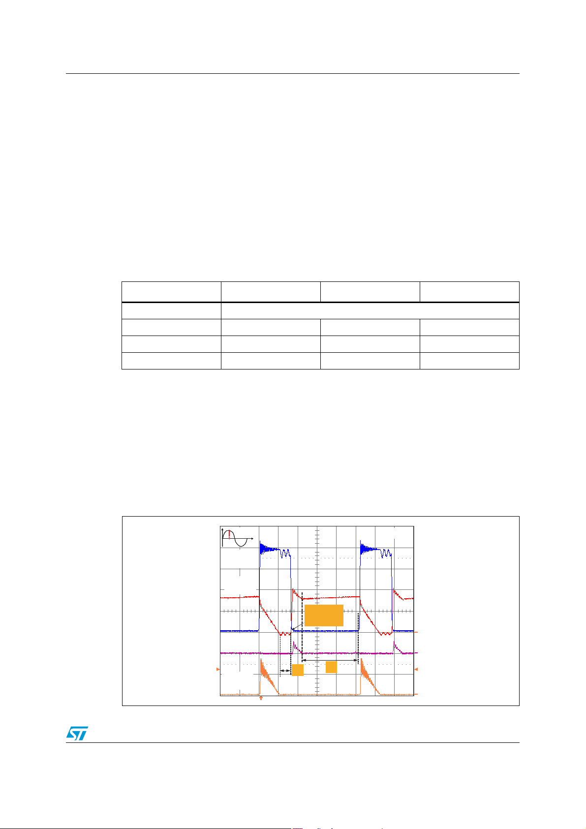
3.2 BC2 typical waveforms
rms 450 W power factor corrector working in hard
mains
52 turns, LB = 600 µH, Tore METGLAS 4520MPEC
Figure 14 shows the typical BC2 waveforms corresponding to a PFC working at 200 kHz.
At each power MOSFET switch-on, soft current switching occurs. This curve highlights that
D
and D2 diodes always work in discontinuous mode; D1 recovers the IRM current from DB
1
whereas D
turns off, the power voltage drain decreases as previously mentioned in the [t
sends the current stored in L through the PFC bulk capacitor. As soon as D2
2
] and [t4-t5]
0-t1
phases and switch-off power losses are saved.
Figure 14. Typical BC
2
waveform at Fs = 200 kHz
Imains(t)
Imains(t)tImains(t)
Tmains
Tmains
t
t
T/4
T/4
V
TR
200V/DIV.
I
L
5A/DIV.
Soft
switching
I
D1
5A/DIV.
t
I
D2
5A/DIV.
D2
1µs/DIV
1 2
3
t
D1
(8t)
4
Doc ID 17975 Rev 1 15/22
BC2 design in 450 W PFC AN3276
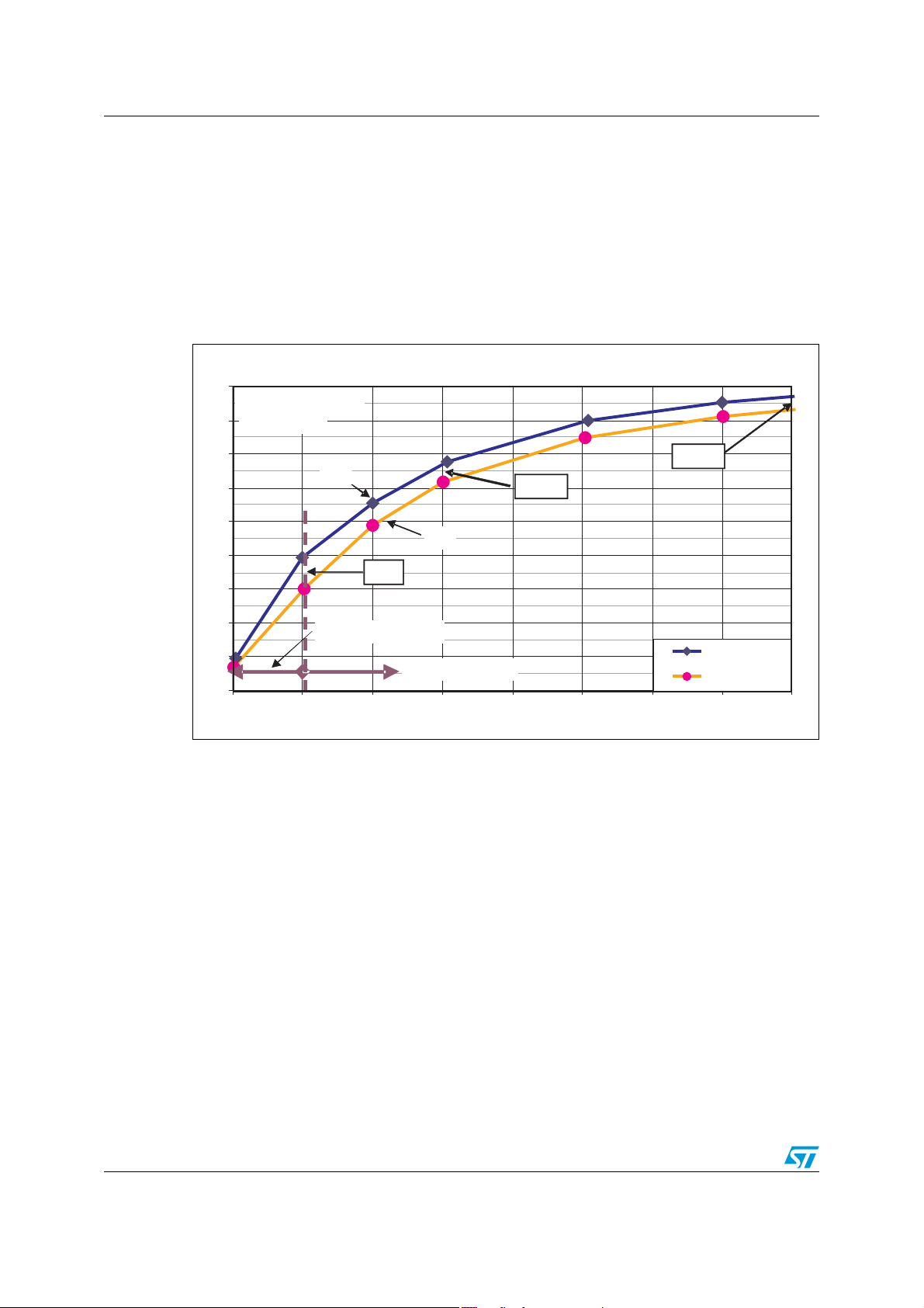
3.3 Efficiency comparison
BC2 and SiC diode efficiency have been compared under two V
Figure 15 (230 V
140kHz. At 230V
) and Figure 16 (90 V
RMS
, the BC2 circuit saves up to 2.25 W at full load and 1 W at 100 W
RMS
) with a switching frequency equal to
RMS
compared to the 8 A SiC diode. Under low load, the reflected voltage from N
the BC
phase time [t
the BC
2
efficiency because the switch-off losses are lower than the SiC as described in the
]. As soon as the PFC works in discontinuous mode (< 100 W) the SiC and
0-t1
2
have the same efficiency as shown in Figure 15.
levels as shown in
mains
S2
still improves
Figure 15. Efficiency comparison at 230 V rms
%
97
96
Fs = 140 kHz
95
V = 230 V
mains RMS
Efficiency = f(P )
OUT
+0.5%
BC²
94
93
+0.7%
SiC
92
+1%
91
90
89
88
50 100 150 200 250 300 350 400 450
Discontinuous mode
Continuous mode
BC² solution
8A SIC
P
OUT
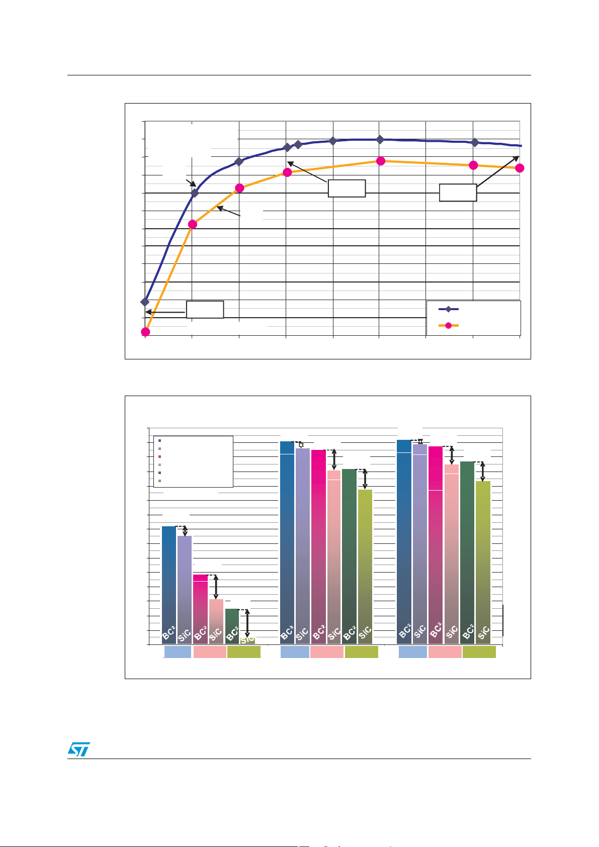
At 90 V rms, the soft switching method benefits plus the power saving in the C
reinforces the benefit of the BC
2
circuit. Up to 5.4 W is saved thanks to the BC2 at 450 W
compared to the SiC diode and under low load, up to 1.7% is saved thanks to the switch-off
power saving.
16/22 Doc ID 17975 Rev 1
discharge
OSS
AN3276 BC2 design in 450 W PFC
Figure 16. Efficiency comparison at 90 V rms
%
95
94
Fs = 140 kHz
93
92
91
V = 90 V
mains RMS
BC²
Efficiency = f(P )
OUT
+1.5%
+1.2%
90
SiC
89
88
87
86
85
84
83
+1.7%
Continuous mode
50 100 150 200 250 300 350 400 450
Figure 17. 450 W PFC efficiency versus three different output powers and three
switching frequencies for V
mains
rms = 90 V
BC² solution
8A SIC
P
OUT
Efficiency=f(POUT,Fs)
%
95
BC² solution 72kHz
94
8A SIC 72kHz
BC² solution 144kHz
93
8A SIC 144kHz
92
BC² solution 200kHz
8A SIC 200kHz
91
Vmains=90VRMS
90
89
+0.7%
88
87
86
85
84
83
82
81
80
FS= FS= FS=
72KHz 72KHz 72KHz140KHz 140KHz 200KHz200KHz 200KHz140KHz
+1.7%
+2%
52 203 400
POUT=50W
Figure 17 highlights the benefit of the BC
Efficiency=f(POUT,Fs)
+0.5%
+1.5%
POUT=200W
2
circuit soft switching method added to its C
discharge power saving especially at low load.
+1.6%
+0.4%
+1.2%
POUT=400W
+1.5%
POUT
OSS
Doc ID 17975 Rev 1 17/22

BC2 design in 450 W PFC AN3276
3.4 Thermal measurement
The soft current switching method allows the power dissipation in the switch transistor to be
reduced. Figure 18 shows that a high thermal temperature difference (18 °C) occurs
between the BC
temperature in the power transistor, the size of the thermal heatsink could be reduced. In
this way, the space saving balances out the space from the small L inductor required by the
2
BC
circuit. Therefore, the BC2 circuit can have the same power density as the SiC diode
solution. Nevertheless, the BC
thermal rising. Figure 18 shows that 0.75 W should be removed from the 5.4 W measured in
the efficiency comparison at 90 V rms. Even in this configuration, the BC
better efficiency than the SiC diode. The BC
efficiency criteria than the SiC diode.
Another consideration is that, for the same thermal heatsink, the Power MOSFET size could
be reduced to further reduce the PFC cost.
Figure 18. Thermal measurement comparison
2
and the SiC diode in the PFC application. For the same working junction
2
efficiency decreases due to the power MOSFET R
2
2
circuit has a better power density and
circuit has a
DS(on)
PFC : V = 90 V
STTH8BC065 diode in the BC² circuit
STTH8BC065DI
Power MOS thermal junction measurement
BC² circuit Tj(avg)= 72 °C
Rdson STP20NM50 Rdson= 0.26 Ω
TR Cond. losses (0.26/2)x4.28² =2.38W
mains RMS
STP20NM50
DB
, Fs = 140 kHz ,
STP20NM50
TR
P = 450 W ,
OUT
DB
Power MOS thermal junction measurement
SiC diode Tj(avg)= 90°C
Rdson STP20NM50 Rdson=0.34Ω
+0.75W
TR Cond. losses (0.34/2)x4.28² = 3.12W
I = 4.28 A , Rg = 47
TRRMS 1
STPSC806D diode in the Boost circuit
STP20NM50
TR
STPSC806D
Ω
STP20NM50
18/22 Doc ID 17975 Rev 1

AN3276 Conclusion
4 Conclusion
The BC2 circuit uses the soft switching method with a unique non-dissipative recovery
circuit. STMicroelectronics has introduced the specific diodes suited for the BC
2
concept to
improve the CCM PFC performance as shown in Ta bl e 4 .
This circuit supports the actual energy efficiency recommendation at 20%, 50% and 100%
of rated power supplies.
Table 4. BC2 benefits in 450 W PFC, 140 kHz
Criteria at 90 V rms SiC diode BC2 circuit Benefits
Efficiency 92.5% 93.7% +1.2%
Power MOSFET
temperature
Power density at
iso-efficiency
EMI
Boost rectification cost > 0.2 € per 100 W >> 0.2 € per 100 W Mass market
90 °C 72 °C -18 °C
State of art Improve, save 5.4 W +1.2% gain
Acceptable with
dI/dt < 1000 A/µs
Acceptable with
dI/dt < 100 A/µs
Soft switching
Doc ID 17975 Rev 1 19/22

References AN3276
5 References
1. Benoît Peron, “Auxiliary switching circuit for a chopping converter”, Patent No: US
6,987,379 B2, June 2006
2. Bertrand Rivet, “New Solution to Optimize Diode Recovery in PFC Boost Converter”,
PCIM 2000.
3. Jim Noon, UC3855A/B High Performance Power Factor Preregulator -Texas
Instrument- application report- SLUA146A
4. Brian T, Irving and M. Jovanovic “Analysis, Design and Performance Evaluation of
Flying-Capacitor Passive Lossless Snubber applied to PFC Boost Converter”, APEC
2002, pp. 503 - 508 vol.1.
20/22 Doc ID 17975 Rev 1

AN3276 Revision history
6 Revision history
Table 5. Document revision history
Date Revision Changes
10-Nov-2010 1 Initial release.
Doc ID 17975 Rev 1 21/22

AN3276
Please Read Carefully:
Information in this document is provided solely in connection with ST products. STMicroelectronics NV and its subsidiaries (“ST”) reserve the
right to make changes, corrections, modifications or improvements, to this document, and the products and services described herein at any
time, without notice.
All ST products are sold pursuant to ST’s terms and conditions of sale.
Purchasers are solely responsible for the choice, selection and use of the ST products and services described herein, and ST assumes no
liability whatsoever relating to the choice, selection or use of the ST products and services described herein.
No license, express or implied, by estoppel or otherwise, to any intellectual property rights is granted under this document. If any part of this
document refers to any third party products or services it shall not be deemed a license grant by ST for the use of such third party products
or services, or any intellectual property contained therein or considered as a warranty covering the use in any manner whatsoever of such
third party products or services or any intellectual property contained therein.
UNLESS OTHERWISE SET FORTH IN ST’S TERMS AND CONDITIONS OF SALE ST DISCLAIMS ANY EXPRESS OR IMPLIED
WARRANTY WITH RESPECT TO THE USE AND/OR SALE OF ST PRODUCTS INCLUDING WITHOUT LIMITATION IMPLIED
WARRANTIES OF MERCHANTABILITY, FITNESS FOR A PARTICULAR PURPOSE (AND THEIR EQUIVALENTS UNDER THE LAWS
OF ANY JURISDICTION), OR INFRINGEMENT OF ANY PATENT, COPYRIGHT OR OTHER INTELLECTUAL PROPERTY RIGHT.
UNLESS EXPRESSLY APPROVED IN WRITING BY AN AUTHORIZED ST REPRESENTATIVE, ST PRODUCTS ARE NOT
RECOMMENDED, AUTHORIZED OR WARRANTED FOR USE IN MILITARY, AIR CRAFT, SPACE, LIFE SAVING, OR LIFE SUSTAINING
APPLICATIONS, NOR IN PRODUCTS OR SYSTEMS WHERE FAILURE OR MALFUNCTION MAY RESULT IN PERSONAL INJURY,
DEATH, OR SEVERE PROPERTY OR ENVIRONMENTAL DAMAGE. ST PRODUCTS WHICH ARE NOT SPECIFIED AS "AUTOMOTIVE
GRADE" MAY ONLY BE USED IN AUTOMOTIVE APPLICATIONS AT USER’S OWN RISK.
Resale of ST products with provisions different from the statements and/or technical features set forth in this document shall immediately void
any warranty granted by ST for the ST product or service described herein and shall not create or extend in any manner whatsoever, any
liability of ST.
ST and the ST logo are trademarks or registered trademarks of ST in various countries.
Information in this document supersedes and replaces all information previously supplied.
The ST logo is a registered trademark of STMicroelectronics. All other names are the property of their respective owners.
© 2010 STMicroelectronics - All rights reserved
STMicroelectronics group of companies
Australia - Belgium - Brazil - Canada - China - Czech Republic - Finland - France - Germany - Hong Kong - India - Israel - Italy - Japan -
Malaysia - Malta - Morocco - Philippines - Singapore - Spain - Sweden - Switzerland - United Kingdom - United States of America
www.st.com
22/22 Doc ID 17975 Rev 1
 Loading...