

Page 1

AN3268
Application note
STM32VLDISCOVERY firmware package
Introduction
The purpose of this application note is to describe the STM32VLDISCOVERY package
structure and provide short descriptions of:
■ STM32VLDISCOVERY firmware demonstration.
■ Examples covering some of the STM32 value line features.
■ Standard firmware library.
The STM32VLDISCOVERY firmware package is available from
http://www.st.com/stm32vldiscovery.
September 2010 Doc ID 17901 Rev 1 1/16
www.st.com
Page 2

Contents AN3268
Contents
1 Package structure . . . . . . . . . . . . . . . . . . . . . . . . . . . . . . . . . . . . . . . . . . . 4
1.1 Libraries . . . . . . . . . . . . . . . . . . . . . . . . . . . . . . . . . . . . . . . . . . . . . . . . . . . 4
1.1.1 CMSIS . . . . . . . . . . . . . . . . . . . . . . . . . . . . . . . . . . . . . . . . . . . . . . . . . . . 5
1.1.2 STM32F10x_StdPeriph_Driver . . . . . . . . . . . . . . . . . . . . . . . . . . . . . . . . 5
1.2 Project . . . . . . . . . . . . . . . . . . . . . . . . . . . . . . . . . . . . . . . . . . . . . . . . . . . . 6
1.3 Utilities . . . . . . . . . . . . . . . . . . . . . . . . . . . . . . . . . . . . . . . . . . . . . . . . . . . . 6
2 STM32VLDISCOVERY firmware examples . . . . . . . . . . . . . . . . . . . . . . . 7
2.1 GPIO toggle example . . . . . . . . . . . . . . . . . . . . . . . . . . . . . . . . . . . . . . . . . 7
2.1.1 Purpose . . . . . . . . . . . . . . . . . . . . . . . . . . . . . . . . . . . . . . . . . . . . . . . . . . 7
2.1.2 Description . . . . . . . . . . . . . . . . . . . . . . . . . . . . . . . . . . . . . . . . . . . . . . . . 7
2.2 RCC (reset and clock control) example . . . . . . . . . . . . . . . . . . . . . . . . . . . 7
2.2.1 Purpose . . . . . . . . . . . . . . . . . . . . . . . . . . . . . . . . . . . . . . . . . . . . . . . . . . 7
2.2.2 Description . . . . . . . . . . . . . . . . . . . . . . . . . . . . . . . . . . . . . . . . . . . . . . . . 8
2.3 EXTI example . . . . . . . . . . . . . . . . . . . . . . . . . . . . . . . . . . . . . . . . . . . . . . . 8
2.3.1 Purpose . . . . . . . . . . . . . . . . . . . . . . . . . . . . . . . . . . . . . . . . . . . . . . . . . . 8
2.3.2 Description . . . . . . . . . . . . . . . . . . . . . . . . . . . . . . . . . . . . . . . . . . . . . . . . 8
2.4 SysTick example . . . . . . . . . . . . . . . . . . . . . . . . . . . . . . . . . . . . . . . . . . . . 9
2.4.1 Purpose . . . . . . . . . . . . . . . . . . . . . . . . . . . . . . . . . . . . . . . . . . . . . . . . . . 9
2.4.2 Description . . . . . . . . . . . . . . . . . . . . . . . . . . . . . . . . . . . . . . . . . . . . . . . . 9
2.5 Low power modes . . . . . . . . . . . . . . . . . . . . . . . . . . . . . . . . . . . . . . . . . . . 9
2.5.1 Standby mode example . . . . . . . . . . . . . . . . . . . . . . . . . . . . . . . . . . . . . . 9
2.5.2 Stop mode example . . . . . . . . . . . . . . . . . . . . . . . . . . . . . . . . . . . . . . . . 10
2.5.3 Sleep mode example . . . . . . . . . . . . . . . . . . . . . . . . . . . . . . . . . . . . . . . 10
2.6 DMA example . . . . . . . . . . . . . . . . . . . . . . . . . . . . . . . . . . . . . . . . . . . . . . 11
2.6.1 Purpose . . . . . . . . . . . . . . . . . . . . . . . . . . . . . . . . . . . . . . . . . . . . . . . . . 11
2.6.2 Description . . . . . . . . . . . . . . . . . . . . . . . . . . . . . . . . . . . . . . . . . . . . . . . 11
2.7 Flash program example . . . . . . . . . . . . . . . . . . . . . . . . . . . . . . . . . . . . . . 11
2.7.1 Purpose . . . . . . . . . . . . . . . . . . . . . . . . . . . . . . . . . . . . . . . . . . . . . . . . . 11
2.7.2 Description . . . . . . . . . . . . . . . . . . . . . . . . . . . . . . . . . . . . . . . . . . . . . . . 11
2.8 IWDG (independant watchdog) example . . . . . . . . . . . . . . . . . . . . . . . . . 12
2.8.1 Purpose . . . . . . . . . . . . . . . . . . . . . . . . . . . . . . . . . . . . . . . . . . . . . . . . . 12
2.8.2 Description . . . . . . . . . . . . . . . . . . . . . . . . . . . . . . . . . . . . . . . . . . . . . . . 12
2/16 Doc ID 17901 Rev 1
Page 3

AN3268 Contents
2.9 WWDG (window watchdog) example . . . . . . . . . . . . . . . . . . . . . . . . . . . . 13
2.9.1 Purpose . . . . . . . . . . . . . . . . . . . . . . . . . . . . . . . . . . . . . . . . . . . . . . . . . 13
2.9.2 Description . . . . . . . . . . . . . . . . . . . . . . . . . . . . . . . . . . . . . . . . . . . . . . . 13
2.10 JTAG remap example . . . . . . . . . . . . . . . . . . . . . . . . . . . . . . . . . . . . . . . . 13
2.10.1 Purpose . . . . . . . . . . . . . . . . . . . . . . . . . . . . . . . . . . . . . . . . . . . . . . . . . 13
2.10.2 Description . . . . . . . . . . . . . . . . . . . . . . . . . . . . . . . . . . . . . . . . . . . . . . . 13
3 STM32VLDISCOVERY demonstration overview . . . . . . . . . . . . . . . . . . 14
4 Revision history . . . . . . . . . . . . . . . . . . . . . . . . . . . . . . . . . . . . . . . . . . . 15
Doc ID 17901 Rev 1 3/16
Page 4
Package structure AN3268
1 Package structure
ST provides a complete development package, the STM32vldiscovery_package, which
allows users to get started easily with the STM32VLDISCOVERY board by simplifying
application code development and execution using the standard peripheral drivers.
This package can be downloaded, together with the user manual, from
http://www.st.com/stm32vldiscovery.
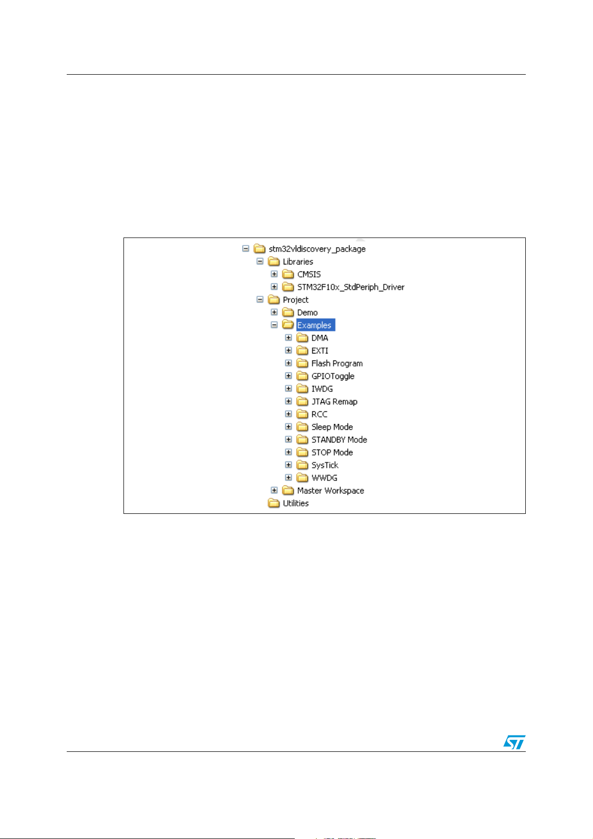
The package is structured as shown in Figure 1.
Figure 1. Stm32vldiscovery_package content
1.1 Libraries
This folder contains all the CMSIS files and the STM32F10x standard peripheral's drivers.
● CMSIS subfolder: Contains the STM32F10xxx CMSIS files: Device Peripheral Access
Layer and Core Peripheral Access Layer.
● STM32F10x_StdPeriph_Driver subfolder: Contains all the subdirectories and files that
make up the core of the library.
4/16 Doc ID 17901 Rev 1
Page 5

AN3268 Package structure
1.1.1 CMSIS
CMSIS (Cortex microcontroller software interface standard) answers the challenges that are
faced when software components are deployed to physical microcontroller devices based on
a Cortex-M0 or Cortex-M3 processor. It is defined in close co-operation with various silicon
and software vendors and provides a common approach to interface with peripherals, realtime operating systems, and middleware components.
ARM provides as part of the CMSIS the following software layers that are available for
various compiler implementations:
● Core Peripheral Access Layer: contains name definitions, address definitions and
helper functions to access core registers and peripherals. It defines also a device
independent interface for RTOS Kernels that includes debug channel definitions. This
software layer is expanded by Silicon partners with:
– Device Peripheral Access Layer: provides definitions for all device peripherals.
– Access functions for peripherals (optional): provides additional helper functions for
peripherals.
CMSIS defines for a Cortex-M microcontroller system:
● A common way to access peripheral registers.
● A common way to define exception vectors.
● Register names of the core peripherals and the names of the core exception vectors.
● An device independent interface for RTOS kernels including a debug channel.
By using CMSIS compliant software components, the user can easier re-use template code.
CMSIS enables the combination of software components from multiple middleware vendors.
1.1.2 STM32F10x_StdPeriph_Driver
This driver corresponds to the STM32F10x Standard Peripherals Library:
http://www.st.com/stonline/products/support/micro/files/stm32f10x_stdperiph_lib.zip.
It is a complete firmware package, consisting of device drivers for all of the standard device
peripherals, for STM32 value line (medium and low), Connectivity line, XL-, high-, mediumand low- density device 32-bit Flash microcontrollers.
The device drivers contain a collection of routines, data structures and macros covering the
features of STM32 peripherals. It includes a description of the device drivers plus a set of
examples for each peripheral. The firmware library allows any device to be used in the user
application without the need for in-depth study of each peripheral’s specification.
Using the Standard Peripherals Library has two advantages: it saves significant time that
would otherwise be spent in coding, while simultaneously reducing application development
and integration costs.
The STM32F10x Standard Peripherals library covers 3 abstraction levels, and includes:
● A complete register address mapping with all bits, bit fields and registers declared in C.
This avoids a cumbersome task and more important, it brings the benefits of a bug free
reference mapping file, speeding up the early project phase.
● A collection of routines and data structures which covers all peripheral functions
(drivers with common API). It can be used directly as a reference framework, since it
also includes macros for supporting core-related intrinsic features and common
constants and data type definitions.
Doc ID 17901 Rev 1 5/16
Page 6

Package structure AN3268
● A set of examples covering all available peripherals with template projects for the most
common development toolchains. These examples are developed to run on an STM32
device with STMicroelectronics STM32 evaluation boards. They should be considered
as example code from which to develop your own application. Some examples have
already been tailored to run on the STM32VLDISCOVERY. They are available from the
STM32VLDISCOVERY web page at http://www.st.com/stm32vldiscovery.
An online help, stm32f10x_stdperiph_lib_um.chm, is available inside the firmware
installation directory to provide you more details about the library structure.
Figure 2. STM32 firmware library online help home page
1.2 Project
This contains three subfolders:
● Master Worskpace: A multi-project workspace allowing you to define a group of
projects in one project workspace window. You can switch from one project to another.
● Demo: Contains a pre-configured project for IAR, MDK-ARM and TrueSTUDIO
toolchains and source/header files corresponding to the demo preprogrammed in the
STM32VLDISCOVERY board.
● Examples: Contains examples. For each example, a pre-configured project for IAR,
MDK-ARM and TrueStudio toolchains and source/header files are provided.
1.3 Utilities
This contains the driver stm32vldiscovery.c which provides an API to interact with the user
push button USER and the LEDs LD3 and LD4 on the STM32DISCOVERY board while
these resources hardware definitions are made in the header file stm32vldiscovery.h.
6/16 Doc ID 17901 Rev 1
Page 7

AN3268 STM32VLDISCOVERY firmware examples
2 STM32VLDISCOVERY firmware examples
Note: 1 No additional hardware is required to make these examples run on the
STM32VLDISCOVERY board.
2 GPIOC pins 8 and 9 are connected respectively to LD4 and LD3 on the
STM32VLDISCOVERY board.
3 GPIOA pin 0 is connected to the USER push button on the STM32VLDISCOVERY board.
2.1 GPIO toggle example
2.1.1 Purpose
This example shows how to use GPIO port bit set/reset registers (BSRR and BRR) for I/O
toggling.
2.1.2 Description
In this example:
● GPIOC clock is enabled.
● GPIOC pins 8 and 9 are configured.
● In a while loop, the ODR8 and ODR9 bits are set in the GPIOC output data register
(ODR) by setting the corresponding bits in the port bit set/reset register (BSRR) and
then the ODR8 and ODR9 bits are reset in the GPIOC output data register (ODR) by
setting the corresponding bits in the port bit reset register (BRR).
● A delay is inserted between setting and resetting the GPIOC ODR8 and ODR9 bits.
When the program is executed, the two LEDs LD3 and LD4 are turned ON then OFF in an
infinite loop. The duration between the ON and OFF states corresponds to the inserted
delay.
2.2 RCC (reset and clock control) example
2.2.1 Purpose
Three different clock sources can be used to drive the system clock (SYSCLK):
● HSI RC internal.
● HSE (high speed external) oscillator.
● PLL: multiplies the HSI RC output or HSE crystal output clock frequency.
This example shows how to use the HSE or PLL as sources to drive the system clock.
Doc ID 17901 Rev 1 7/16
Page 8

STM32VLDISCOVERY firmware examples AN3268
2.2.2 Description
The system frequency is selected by the user in main.h.
In main.h, you choose the source which drives the system clock by uncommenting a line of
code:
● uncomment ‘#define SYSCLK_HSE’ to use HSE as source.
● uncomment ‘#define SYSCLK_FREQ_24MHz’ to use PLL as source.
In order to use the HSE as source to drive the system clock:
1. Enable HSE.
2. Wait until HSE is ready.
3. Configure the AHB, APB1 and APB2 prescalers to define the AHB, APB1 and APB2
frequencies.
4. Select the HSE as system clock source.
5. Wait until HSE is used as system clock source.
In order to use the PLL as source to drive the system clock (in this example, the PLL
multiplies the HSE output clock frequency)
1. Enable HSE.
2. Wait until HSE is ready.
3. Configure the AHB, APB1 and APB2 prescalers to define the AHB, APB1 and APB2
frequencies.
4. Configure the PLL factors.
5. Enable the PLL and waits until the PLL is ready.
6. Select the PLL as system clock source.
7. Wait until PLL is used as system clock source.
2.3 EXTI example
2.3.1 Purpose
This example shows how to configure an external interrupt line.
2.3.2 Description
In this example:
● PA0 pin is configured in input floating.
● PA0 is configured to be used as external interrupt source line 0 (EXTI0).
● The EXTI line 0 is configured to generate an interrupt on each falling edge detected on
PA0 pin. This means that the interrupt is triggered every time the USER push button is
pressed.
● In the NVIC (nested vectored interrupt controller), the EXTI line 0 interrupt priority is
configured and the interrupt is enabled.
● Inside the EXTI0 interrupt routine, the PC9 pin is toggled.
8/16 Doc ID 17901 Rev 1
Page 9

AN3268 STM32VLDISCOVERY firmware examples
2.4 SysTick example
2.4.1 Purpose
This example shows how to configure system tick and use it to generate a 1 ms time base.
2.4.2 Description
In this example:
● The system tick timer is initialized.
● The system tick timer interrupt is enabled in the NVIC.
● System tick timer/counter starts in free running mode to generate periodical interrupts.
● The system tick timer interrupt is triggered every 1 ms.
● A "Delay" function is implemented based on the system tick timer end-of-count event.
The two LEDs LD3 and LD4 are toggled with a timing defined by the Delay function.
2.5 Low power modes
The STM32F100 device features three low-power modes: Sleep mode, Stop mode, and
Standby mode.
Note: STM32F100RBT6B consumption can be measured on the STM32VLDiscovery board by
removing jumper JP1, labeled IDD, and connecting an ammeter.
2.5.1 Standby mode example
Purpose
This example shows how Stop mode is entered and exited using EXTI line interrupts.
Description
In this example:
● The real-time clock (RTC) alarm is used to wake up the system from Standby mode.
● The EXTI line 0 is configured to generate interrupt on falling edge.
● SysTick is programmed to generate an interrupt every 250 ms. In the SysTick interrupt
handler, LD3 is toggled to indicate whether the MCU is in Standby or Run mode.
● When the USER push button is pressed on the STM32VLDISCOVERY board, a falling
edge is detected on the EXTI line 0 and an interrupt is generated.
● In the EXTI line 0 handler routine, the real-time clock is configured to generate an
alarm event in 3 seconds, then the system enters Standby mode using the WFI entry
mode, causing the LED3 to stop toggling.
● An external RESET wakes up the system from Standby. If within 3 seconds an external
RESET is not generated, the real-time clock alarm wakes up the system.
On the STM32VLDISCOVERY board:
● LD3 is toggling: the system is in Run mode.
● LD3 is off and LD4 is off: system is in Standby mode.
● LD4 is on: the system resumed from Standby mode.
Doc ID 17901 Rev 1 9/16
Page 10

STM32VLDISCOVERY firmware examples AN3268
2.5.2 Stop mode example
Purpose
This example shows how Stop mode is entered and exited using EXTI line interrupts.
Description
In this example:
● The EXTI line 0 and the EXTI line 17 (real-time clock alarm) interrupts are used to wake
up the system from Stop mode.
● The EXTI line 0 is configured to generate an interrupt on falling edge.
● The EXTI line17 (real-time clock alarm) is configured to generate an interrupt on rising
edge and the real-time clock time base is set to 1 second using the external low speed
oscillator (LSE).
● The system enters and exits Stop mode as following:
– After 2 seconds from system start-up, the real-time clock is configured to generate
an alarm event in 3 seconds, then the system enters Stop mode using the WFI
entry mode.
– The system wakes up Stop mode, either when detecting a falling edge on EXTI
line 0 (USER push button is pressed) or by real-time clock alarm which wakes up
the system within 3 seconds.
● After exiting from Stop, the system clock is reconfigured to its previous state (as HSE
and PLL are disabled in Stop mode).
On the STM32VLDISCOVERY board,:
● LD3 is on: the system is in Run mode.
● LD3 is off: the system is in Stop mode.
● LD4 is on: EXTI Line 0 is used to exit from Stop mode.
● LD4 is off: EXTI line17 (real-time clock alarm) is used to exit from Stop mode.
2.5.3 Sleep mode example
Purpose
This example shows how Sleep mode is entered and exited using EXTI line interrupt.
Description
In this example:
● The Sleep mode is entered using the WFI entrymode.
● The EXTI line 0 is configured to generate interrupt on falling edge (after the USER push
button is pressed on the STM32VLDISCOVERY board, a falling edge is detected on the
EXTI line 0 and an interrupt is generated).
● When the EXTI line 0 interrupt is served, the system wakes up from Sleep mode.
10/16 Doc ID 17901 Rev 1
Page 11

AN3268 STM32VLDISCOVERY firmware examples
2.6 DMA example
2.6.1 Purpose
This example ishows how to use a DMA channel to transfer a word data buffer from Flash
memory to embedded SRAM memory.
2.6.2 Description
In this example, the DMA1 Channel 6 is configured to transfer the contents of a 32-word
data buffer stored in Flash memory to a buffer in RAM. For this purpose, in the main.c
source file:
● The DMA1 Channel 6 is configured:
– Source and destination base addresses are configured (the source is the buffer in
Flash and the destination is the buffer in RAM).
– Memory-to-memory transfer is enabled.
– Source and destination address incrementing is enabled.
– The number of data words is configured (32).
– The DMA mode is configured (Normal mode).
● The DMA1 channel 6 transfer complete interrupt is enabled.
● The transfer is started by setting the channel enable bit for DMA1 Channel 6.
● The firmware waits until the DMA1 channel 6 end of transfer by waiting until the
CurrDataCounterEnd variable reaches 0 (the CurrDataCounterEnd variable is
read inside the DMA1 channel 6 transfer complete interrupt routine which is serviced
when the number of data being transferred reaches 0).
● Once the CurrDataCounterEnd variable is found equal to 0, a comparison between
the source and destination buffers is done to check if all data have been correctly
transferred or not.
2.7 Flash program example
2.7.1 Purpose
This example provides a description of how to program the STM32 value line internal Flash.
2.7.2 Description
After reset, the Flash program and erase controller is protected. An unlocking sequence
should be written to the FLASH_KEYR register prior to any program or erase operation.
Doc ID 17901 Rev 1 11/16
Page 12

STM32VLDISCOVERY firmware examples AN3268
2.8 IWDG (independant watchdog) example
2.8.1 Purpose
This example shows how to reload the independant watchdog counter at regulate periods
using the system tick and how the independant watchdog reset is generated.
2.8.2 Description
In this example:
● The independant watchdog timeout is set to 280 ms.
● The system tick is configured to generate an interrupt every 250 ms.
● In the system tick interrupt service routine, the independant watchdog counter is
reloaded to prevent an independant watchdog reset, and LD4 is toggled.
● EXTI line 0 is connected to PA0 pin and configured to generate an interrupt on its falling
edge.
● In the NVIC, this EXTI line 0 correspondant interrupt vector is enabled with a priority
equal to 0, and the systick interrupt vector priority is set to 1 i.e. EXTI interrupt is prior
to systick interrupt.
● The EXTI line is used to simulate a firmware failure: when the EXTI line event is
triggered (after pressing the USER push-button on the STM32VLDISCOVERY board),
the corresponding interrupt is served. In the ISR, the LD3 turns off and the EXTI line
pending bit is not cleared. So the CPU executes the EXTI line ISR indefinitely and the
system tick interrupt routine is never entered so the independant watchdog counter is
not reloaded. As a result, when the independant watchdog counter reaches 00X, the
independant watchdog generates a reset.
● When the independant watchdog reset is generated, LD3 is turned on after the system
resumes operation.
12/16 Doc ID 17901 Rev 1
Page 13

AN3268 STM32VLDISCOVERY firmware examples
2.9 WWDG (window watchdog) example
2.9.1 Purpose
This example shows how to update the WWDG counter at regulate periods using the early
wakeup interrupt (EWI).
2.9.2 Description
In this example:
● Internal watchdog timeout is set to 87.42 ms.
● WWDG timeout is set to 87.42ms. The refresh window is set to 65 and EWI is enabled.
● When the WWDG counter reaches 64, the EWI is generated. In the WWDG interrupt
routine, the counter is refreshed to prevent a WWDG reset.
● EXTI Line 0 is connected to PA0 pin, and configured to generate an interrupt on the
falling edge of the signal.
● In the NVIC, the EXTI line interrupt vector is enabled with a priority equal to 0 and the
WWDG interrupt vector is enabled with a priority equal to 1 i.e. EXTI interrupt is prior to
systick interrupt.
● The EXTI line is used to simulate a firmware failure: once the EXTI Line event occurs,
after pressing the USER push-button on the STM32VLDISCOVERY board, the
corresponding interrupt is served.
● In the EXTI interrupt routine, the EXTI line pending bit is not cleared, so the CPU
executes the EXTI line interrupt routine indefinitely and the WWDG interrupt routine is
never executed (the WWDG counter is not updated).
● As a result, when the WWDG counter falls to 63, the WWDG reset occurs.
● If EXTI line event does not occur (USER push button is not pressed), the WWDG
counter is indefinitely refreshed in WWDG interrupt routine, there is no WWDG reset.
2.10 JTAG remap example
2.10.1 Purpose
This example provides a short description of how to remap the JTAG pins and use them as
standard GPIOs.
2.10.2 Description
It is possible to use the JTAG pins (PA.13(JTMS/SWDAT), PA.14(JTCK/SWCLK),
PA.15(JTDI), PB.03(JTDO) and PB.04(JTRST)) pins as standard GPIOs.
● First, JTAG is disabled using GPIO_PinRemapConfig routine from the standard library.
● Then, all JTAG pins are configured as output push/pull and toggled inside a while loop.
● Once the JTAG I/Os are disabled, connection with the host debugger is lost and cannot
be re-established as long as the JTAG I/Os remain disabled.
● The pin PA0 is used to disable (or not) the JTAG I/Os:
– USER button pressed at reset: JTAG I/Os disabled and LED LD3 turned on.
– USER button not pressed at reset: JTAG I/Os unchanged and LED LD4 turned on.
Doc ID 17901 Rev 1 13/16
Page 14

STM32VLDISCOVERY demonstration overview AN3268
3 STM32VLDISCOVERY demonstration overview
In this demonstration, a check on the LSE status is performed:
● In the case of failure, LED 4 is turned on.
● In the case of success, the PC9 pin is toggled. Its toggling frequency changes
according to the PA0 pin level, that is, the LD3 blinking changes according to the USER
push button clicks. Each click on the USER push button is confirmed by the LD4.
14/16 Doc ID 17901 Rev 1
Page 15

AN3268 Revision history
4 Revision history
Table 1. Document revision history
Date Revision Changes
09-Sept-2010 1 Initial release.
Doc ID 17901 Rev 1 15/16
Page 16

AN3268
Please Read Carefully:
Information in this document is provided solely in connection with ST products. STMicroelectronics NV and its subsidiaries (“ST”) reserve the
right to make changes, corrections, modifications or improvements, to this document, and the products and services described herein at any
time, without notice.
All ST products are sold pursuant to ST’s terms and conditions of sale.
Purchasers are solely responsible for the choice, selection and use of the ST products and services described herein, and ST assumes no
liability whatsoever relating to the choice, selection or use of the ST products and services described herein.
No license, express or implied, by estoppel or otherwise, to any intellectual property rights is granted under this document. If any part of this
document refers to any third party products or services it shall not be deemed a license grant by ST for the use of such third party products
or services, or any intellectual property contained therein or considered as a warranty covering the use in any manner whatsoever of such
third party products or services or any intellectual property contained therein.
UNLESS OTHERWISE SET FORTH IN ST’S TERMS AND CONDITIONS OF SALE ST DISCLAIMS ANY EXPRESS OR IMPLIED
WARRANTY WITH RESPECT TO THE USE AND/OR SALE OF ST PRODUCTS INCLUDING WITHOUT LIMITATION IMPLIED
WARRANTIES OF MERCHANTABILITY, FITNESS FOR A PARTICULAR PURPOSE (AND THEIR EQUIVALENTS UNDER THE LAWS
OF ANY JURISDICTION), OR INFRINGEMENT OF ANY PATENT, COPYRIGHT OR OTHER INTELLECTUAL PROPERTY RIGHT.
UNLESS EXPRESSLY APPROVED IN WRITING BY AN AUTHORIZED ST REPRESENTATIVE, ST PRODUCTS ARE NOT
RECOMMENDED, AUTHORIZED OR WARRANTED FOR USE IN MILITARY, AIR CRAFT, SPACE, LIFE SAVING, OR LIFE SUSTAINING
APPLICATIONS, NOR IN PRODUCTS OR SYSTEMS WHERE FAILURE OR MALFUNCTION MAY RESULT IN PERSONAL INJURY,
DEATH, OR SEVERE PROPERTY OR ENVIRONMENTAL DAMAGE. ST PRODUCTS WHICH ARE NOT SPECIFIED AS "AUTOMOTIVE
GRADE" MAY ONLY BE USED IN AUTOMOTIVE APPLICATIONS AT USER’S OWN RISK.
Resale of ST products with provisions different from the statements and/or technical features set forth in this document shall immediately void
any warranty granted by ST for the ST product or service described herein and shall not create or extend in any manner whatsoever, any
liability of ST.
ST and the ST logo are trademarks or registered trademarks of ST in various countries.
Information in this document supersedes and replaces all information previously supplied.
The ST logo is a registered trademark of STMicroelectronics. All other names are the property of their respective owners.
© 2010 STMicroelectronics - All rights reserved
STMicroelectronics group of companies
Australia - Belgium - Brazil - Canada - China - Czech Republic - Finland - France - Germany - Hong Kong - India - Israel - Italy - Japan -
Malaysia - Malta - Morocco - Philippines - Singapore - Spain - Sweden - Switzerland - United Kingdom - United States of America
www.st.com
16/16 Doc ID 17901 Rev 1
 Loading...