

Page 1

AN3267
Application note
Impact of power MOSFET VGS on buck converter performance
Introduction
DC-DC buck converters are widely used in the computer and peripherals industry due to
their high efficiency and simple electrical topology. In synchronous buck converter design
and semiconductor device choice, converter efficiency maximization and switching behavior
immunity to voltage stresses and fast transients are mandatory.
This document presents the simulation and experimental test results on a single-phase
synchronous buck converter, highlighting the power MOSFET gate driving voltage impact on
converter power management and switching behavior. In the latest generation of
microprocessors for desktops and mobile equipment, ever increasing switching frequency
and output current delivered to the CPU have become necessary.
These features push converter and system designers to critical choices for overall
performance optimization. In fact, fast transients, together with high load currents, may
degrade the converter thermal and power management. Therefore, a deep and accurate
fine tuning of the main electrical parameters is mandatory. In this document, based on the
single-phase synchronous buck converter topology, the impact of different power MOSFET
gate-source voltages on converter efficiency and waveforms of main circuit nodes is
thoroughly analyzed through OrCAD
perfect match between these two experiments.
®
simulations and bench test results, highlighting a
August 2011 Doc ID 17890 Rev 1 1/19
www.st.com
Page 2

Contents AN3267
Contents
1 Synchronous buck converter basic principles . . . . . . . . . . . . . . . . . . . . 4
2 Power MOSFET gate driving voltage requirements in real applications
. . . . . . . . . . . . . . . . . . . . . . . . . . . . . . . . . . . . . . . . . . . . . . . . . . . . . . . . . . . 6
3 Synchronous buck converter testing demonstration board . . . . . . . . . 7
3.1 HS/LS switching behavior evaluation and phase node spike measurements
. . . . . . . . . . . . . . . . . . . . . . . . . . . . . . . . . . . . . . . . . . . . . . . . . . . . . . . . . . 8
3.2 Converter efficiency calculation . . . . . . . . . . . . . . . . . . . . . . . . . . . . . . . . 13
4 Conclusions . . . . . . . . . . . . . . . . . . . . . . . . . . . . . . . . . . . . . . . . . . . . . . . 16
5 References . . . . . . . . . . . . . . . . . . . . . . . . . . . . . . . . . . . . . . . . . . . . . . . . 17
6 Revision history . . . . . . . . . . . . . . . . . . . . . . . . . . . . . . . . . . . . . . . . . . . 18
2/19 Doc ID 17890 Rev 1
Page 3

AN3267 List of figures
List of figures
Figure 1. Single-phase synchronous buck converter topology . . . . . . . . . . . . . . . . . . . . . . . . . . . . . . 4
Figure 2. Testing demonstration board schematic . . . . . . . . . . . . . . . . . . . . . . . . . . . . . . . . . . . . . . . . 7
Figure 3. Power MOSFET waveforms @ 5 V . . . . . . . . . . . . . . . . . . . . . . . . . . . . . . . . . . . . . . . . . . . 8
Figure 4. Power MOSFET waveforms @ 12 V . . . . . . . . . . . . . . . . . . . . . . . . . . . . . . . . . . . . . . . . . . 9
Figure 5. Phase node overshoot comparison . . . . . . . . . . . . . . . . . . . . . . . . . . . . . . . . . . . . . . . . . . . 9
Figure 6. Phase node vs. power MOSFET gate driving voltage . . . . . . . . . . . . . . . . . . . . . . . . . . . . 10
Figure 7. Phase node @ 5 V / 12 V . . . . . . . . . . . . . . . . . . . . . . . . . . . . . . . . . . . . . . . . . . . . . . . . . . 10
Figure 8. HS / LS signal comparison . . . . . . . . . . . . . . . . . . . . . . . . . . . . . . . . . . . . . . . . . . . . . . . . . 10
Figure 9. HS turn-on waveform @ 12 V . . . . . . . . . . . . . . . . . . . . . . . . . . . . . . . . . . . . . . . . . . . . . . . 11
Figure 10. HS turn-on waveform @ 5 V . . . . . . . . . . . . . . . . . . . . . . . . . . . . . . . . . . . . . . . . . . . . . . . . 11
Figure 11. Clamped inductive switching circuit . . . . . . . . . . . . . . . . . . . . . . . . . . . . . . . . . . . . . . . . . . 11
Figure 12. Rise time vs. power MOSFET G-S voltage. . . . . . . . . . . . . . . . . . . . . . . . . . . . . . . . . . . . . 12
Figure 13. Impact of V
Figure 14. Efficiency comparison . . . . . . . . . . . . . . . . . . . . . . . . . . . . . . . . . . . . . . . . . . . . . . . . . . . . . 14
Figure 15. Thermal capture @ 16 A. . . . . . . . . . . . . . . . . . . . . . . . . . . . . . . . . . . . . . . . . . . . . . . . . . . 15
on power MOSFET R
GS
. . . . . . . . . . . . . . . . . . . . . . . . . . . . . . . . . . . . 13
DS(on)
Doc ID 17890 Rev 1 3/19
Page 4
Synchronous buck converter basic principles AN3267
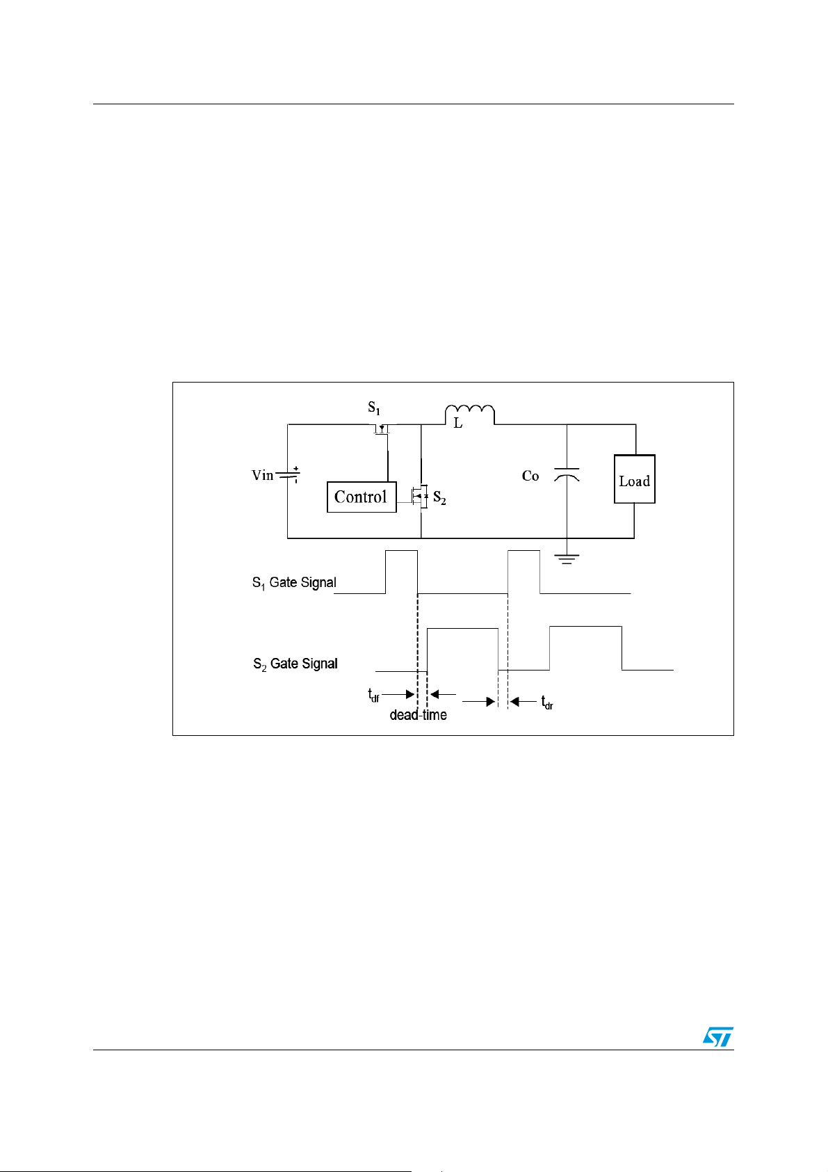
1 Synchronous buck converter basic principles
The synchronous buck converter is the most common electrical topology used for DC-DC
converters which supply a CPU. In Figure 1, the basic schematic is depicted, where:
● S1 is the control FET (or high side FET)
● S2 is the synchronous FET (or low side FET).
In Figure 1 it is also possible to see that the power MOSFET’s gate signals are provided by
the “control unit” in a synchronous way: S1 and S2 cannot be in an on-state simultaneously,
avoiding the creation of a low-resistance path between the input voltage (V
) and GND
IN
(shoot-through or cross-conduction), and generating a spurious power dissipation which
worsens overall efficiency.
Figure 1. Single-phase synchronous buck converter topology
L and Co form the output filter (low-pass filter), which generates a DC voltage from a
square-wave signal on the low side drain (so-called phase node). The synchronous buck
converter is a closed-loop topology as the output voltage is compared firstly with a reference
voltage, producing an error signal; this voltage is then compared to a sawtooth signal, at the
desired switching frequency (f
) (integrated in the control unit) to switch the power
sw
MOSFETs on and off. In this way, the output voltage is stable when line or load changes
occur.
Together with the output voltage regulation, the control unit provides complete logic control
and various protections such as overcurrent, overvoltage, undervoltage, etc.
When S1 is ON, the current in the output coil increases linearly (dI/dt = (V
VL = V
- V
IN
. During dead time (tdf), the energy store in L discharges through the body-
OUT
drain diode of S2 until its gate-source signal becomes high. Therefore, the load current
diverts from the body-drain diode to the channel (V
signals are low and the body-drain diode is forward-biased, allowing the load current flow.
4/19 Doc ID 17890 Rev 1
DS,ON
<< V
F, D IO D E
AM07212v1
IN-VOUT
)/ L a nd
). Finally, both gate
Page 5

AN3267 Synchronous buck converter basic principles
During dead time and before HS turn-on, the LS device must remove the charge stored in
the LS body-drain diode (reverse recovery charge process) before sustaining drain-source
voltage. Therefore, the body-drain characteristics, in terms of reverse recovery current and
charge, heavily impact the power MOSFET’s switching behavior and converter power
losses, especially when the converter switching frequency rises.
In a synchronous buck converter, the low side drain is subjected to fast positive/negative
slopes and high voltage spikes, which can exceed the low side absolute maximum voltage,
degrading power MOSFET reliability up to its failure. For this reason, the right power
MOSFET choice and system configuration, placing of the device on the board and the
optimization of the stray inductances and parasitic, allow important phase node spike
reduction, improving converter performance.
The input-output relationship of a buck converter is given by:
Equation 1
V
OUT
DV
=
IN
D is the converter duty cycle, defined as the ratio between the ON time of the HS and the
switching period.
Doc ID 17890 Rev 1 5/19
Page 6

Power MOSFET gate driving voltage requirements in real applications AN3267
2 Power MOSFET gate driving voltage requirements in
real applications
In common synchronous buck converter topologies, two different solutions are widely used
for the power MOSFET gate signal generation: driver and PWM logic controller integration in
a single package or separately mounting the PWM logic controller and power MOSFET
driver to turn the power switches on and off. The main controller suppliers provide a large
number of products for both solutions.
The gate-source voltages, needed to turn the high side and low side devices on and off, are
generated by the driver section, formed by a common push-pull circuit. Typically, these
voltages are chosen in the range of 5 V to 10 V, depending on application features: switching
frequency, converter efficiency target, maximum load current, power MOSFET number and
electrical characteristics, driver DC power consumption minimization, and system power
limitations. Typically, desktop applications need 10 V as the power MOSFET gate driving
voltage, because currents delivered to the load are high and the output voltage becomes
lower and lower (up to 1 V). In these operating conditions, low side devices are in the onstate for the majority of a switching period, so the conduction losses must be minimized to
improve the system power management: lower on-state losses mean lower R
higher V
(up to 10-12 V).
GS
It is the contrary in the mobile segment, 5 V power MOSFET gate-source voltage choice is
due to 5 V supply rail availability (it also feeds USB and HDD sections). In fact, the input
voltage, which varies from 8 V to 19 V, is not suitable for driving power MOSFETs, while
other voltages in the system are lower than 3.3 V and so cannot switch the devices on and
off. In this way, the power MOSFET gate driving voltage is obtained “free”, without additional
active and passive components.
DS(on)
and
6/19 Doc ID 17890 Rev 1
Page 7
AN3267 Synchronous buck converter testing demonstration board
3 Synchronous buck converter testing demonstration
board
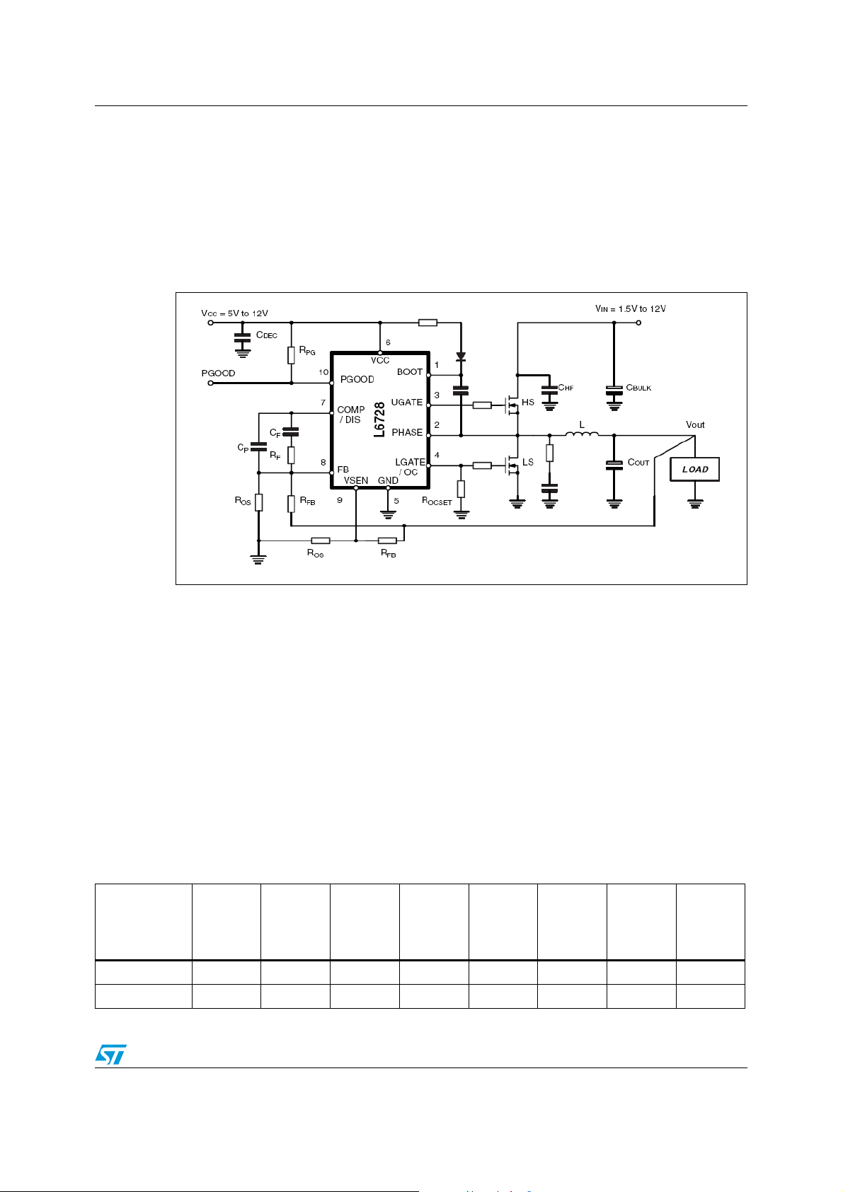
The test vehicle is a synchronous buck converter, which lowers the input voltage (12 V) to
1.25 V as output; the converter switching frequency is 300 kHz (Figure 2), while the
maximum output current is 20 A.
Figure 2. Testing demonstration board schematic
The power MOSFETs are driven by an L6728 single-phase PWM controller with integrated
driver (I
HS,SRC
= 1.5 A, R
HS,SINK
advantage for this analysis is the availability of both the physical board and the full PSpice
model of the converter (including driver and MOSFETs). Based on the same schematic, with
identical passive and semiconductor devices, it is possible to use the converter PSpice
model for testing various operating conditions, validating and explaining the experimental
results. Furthermore, the simulation data are very helpful to evaluate the power MOSFET
currents, because on the real board they cannot be measured by current probes.
As shown in Figure 2, through a different external DC power supply, it is possible to provide
different voltages as the input voltage (V
the impact of the power MOSFET’s gate driving voltage on the converter performance is
thoroughly analyzed, evaluating the power MOSFET switching behavior and thermal
management. The power MOSFETs mounted on the board have the following electrical
characteristics:
Table 1. Power MOSFET electrical characteristics
BV
@
Type
DSS
250 µA
(V)
VSD @
25 mA
(mV)
STD60N3LH5 30 N.A. N.A. 7.3 1450 62 285 1.2
V
@
th
250 µA
(V)
= 1.1 Ω, I
R
DS(on)
10 V
typ.
(mΩ)
AM07213v1
= 1.5 A, R
LS,SRC
) and driver supply voltage (VCC): adjusting VCC,
IN
@
C
iss
LS,SINK
@
15 V
(pF)
= 0.65 Ω). The main
C
rss
15 V
(pF)
@
C
oss
15 V
(pF)
@
R
(Ω)
®
g
STD95N3LLH6 33.8 576 1.55 3.7 2040 271 511 1.2
Doc ID 17890 Rev 1 7/19
Page 8
Synchronous buck converter testing demonstration board AN3267
3.1 HS/LS switching behavior evaluation and phase node spike measurements
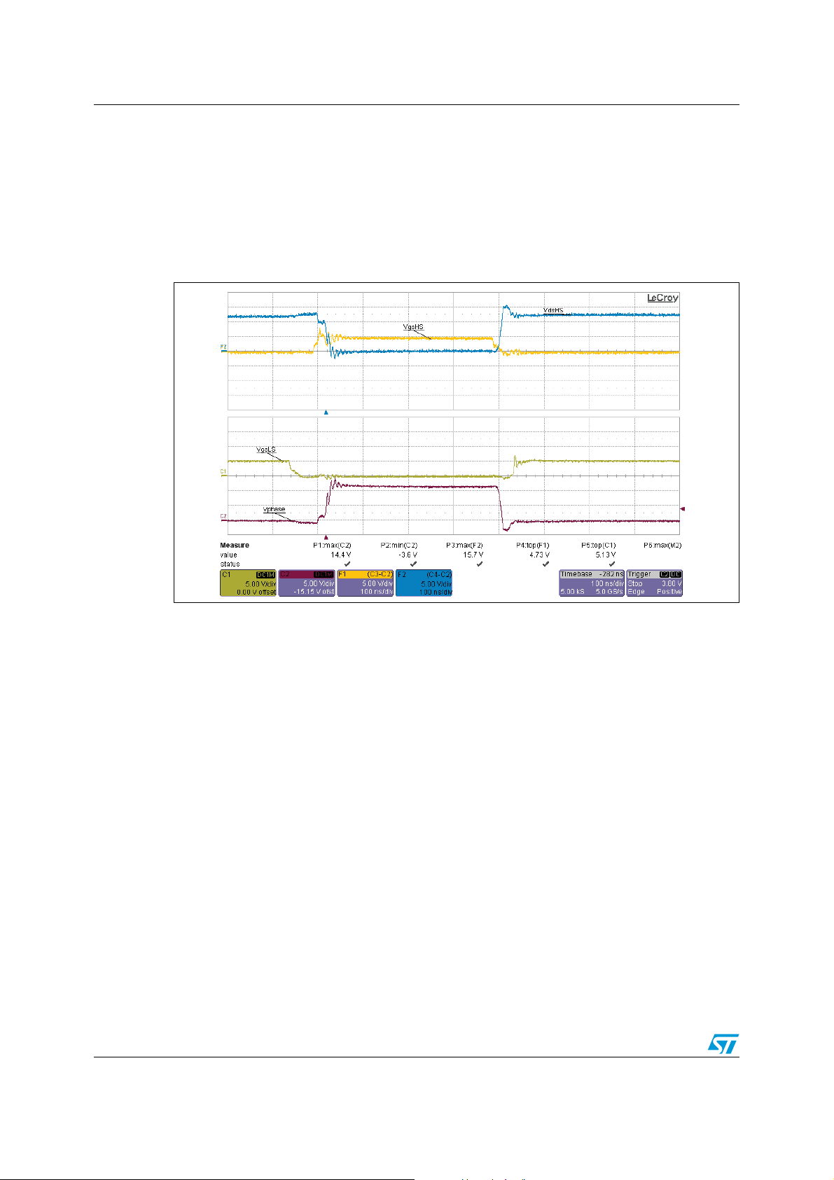
Firstly, the HS/LS switching behavior is analyzed by capturing the relevant MOSFET
waveforms. The maximum output current is fixed at 20 A by an electronic DC load; the
waveforms are captured at maximum load. The MOSFET gate driving voltage is adjusted at
5 V by an external DC power supply.
Figure 3. Power MOSFET waveforms @ 5 V
AM07214v1
The blue and orange traces show HS drain-source and gate-source signals, while the yellow
and purple ones are the LS waveforms. The maximum phase node spike is 14.4 V.
8/19 Doc ID 17890 Rev 1
Page 9

AN3267 Synchronous buck converter testing demonstration board
Figure 4. Power MOSFET waveforms @ 12 V
AM07215v1
Increasing the external driver DC supply, the MOSFET’s gate driving voltage rises to 12 V.
The relevant waveforms are shown in Figure 4.
It is easy to see that the phase node spike overshoot has increased strongly, reaching 25.5
V. Obviously, the converter is working in safe mode because the power MOSFET’s
breakdown voltage is 30 V. Increasing the output current from 0 A to 20 A, with 4 A as step,
both for V
= 5 V and VGS = 12 V, it is possible to link the phase node spike overshoot to
GS
the output current, see Figure 5.
Figure 5. Phase node overshoot comparison
27
24
VGS=12 V
21
17
=5 V
Vphase,max(v)
V
GS
15
12
0
2
468
10
Iout (A)
12
14
16
18
20
22 24
AM07216v1
In the whole current range, driving the power MOSFETs at 5 V, the phase node spike is
strongly reduced, with a maximum value of 16.3 V at 10 A.
By fixing the output current (i.e. 16 A) and varying the power MOSFET’s gate-source
voltage, the chart shown in Figure 6 is obtained.
Doc ID 17890 Rev 1 9/19
Page 10

Synchronous buck converter testing demonstration board AN3267
Figure 6. Phase node vs. power MOSFET gate driving voltage
Phase node ringing @ 16 A
Vgs [V]
AM07217v1
For V
27
24
21
18
Vphase,max (V)
15
12
5678 9101112
Vphase,max @ 16 A
higher than 8 V, the power MOSFET gate driving impact on the phase node spike is
GS
not great, while at lower voltages the overshoot reduction is more evident. In other words,
lower power MOSFET gate voltages are helpful to reduce phase node voltage stress,
improving the power MOSFET reliability and robustness.
Now, the power MOSFET waveforms at two different driving voltages (5 V and 12 V) are
inserted in the same chart to compare them and highlight the main differences. In Figure 7,
the phase node waveforms are compared at the two different operating conditions, while in
Figure 8, HS/LS G-S and phase node signals are given.
Figure 7. Phase node @ 5 V / 12 V Figure 8. HS / LS signal comparison
AM07218v1 AM07219v1
Some relevant differences are easily observed at V
= 5 V. First, looking at the phase node
GS
signal, the “plateau” after the body diode conduction is relatively longer and the maximum
spike is strongly reduced. Comparing the phase node waveforms, it seems that the LS
body-drain diode is in the on-state for a shorter time, therefore the dead time has less
duration (around 10 ns) and the charge stored in the body-drain diode during the reverse
recovery process (Q
) decreases, reducing the voltage stress on the phase node and the
rr
reverse recovery current that adds up to the load current.
The simulation tools can validate these assertions on phase node spike minimization at
lower gate driving voltage. Two different simulations are performed by the full OrCAD model
10/19 Doc ID 17890 Rev 1
Page 11
AN3267 Synchronous buck converter testing demonstration board
of the testing board. The only changing parameter is the driver supply voltage, 5 V and 12 V.
In Figure 9 and 10, the waveforms at HS turn-on for both operating conditions are shown.
Figure 9. HS turn-on waveform @ 12 V Figure 10. HS turn-on waveform @ 5 V
38. 5
20. 0
0
SEL>>
-18.8
I (U1003:Drai n) V( U1003: Drai n) - V(U1003:Source) V(HMG1) - V( PHASE)
38.5
20.0
0
SEL>>
-18. 8
I(U1003:Drain) V( U100 3: Drai n) - V( U1003: Sour ce) V(HMG1) - V( PHAS E)
31
20
0
-13
198.180us 198.200us 198.220us 198. 240us 198.260us 198.280us 198. 300 us 198 . 320u s198. 165us
V( PHASE) - I(U1004:Drain) V( L MG1)
31
20
0
-13
198. 18 0us 19 8. 200 us 198. 220us 198. 2 40us 198. 260us 198. 280us 198. 300us 198. 3 20us198. 1 65us
Ti me
V( PHASE) - I(U1004:Drain) V( L MG1)
AM07220v1
Ti me
AM08141v1
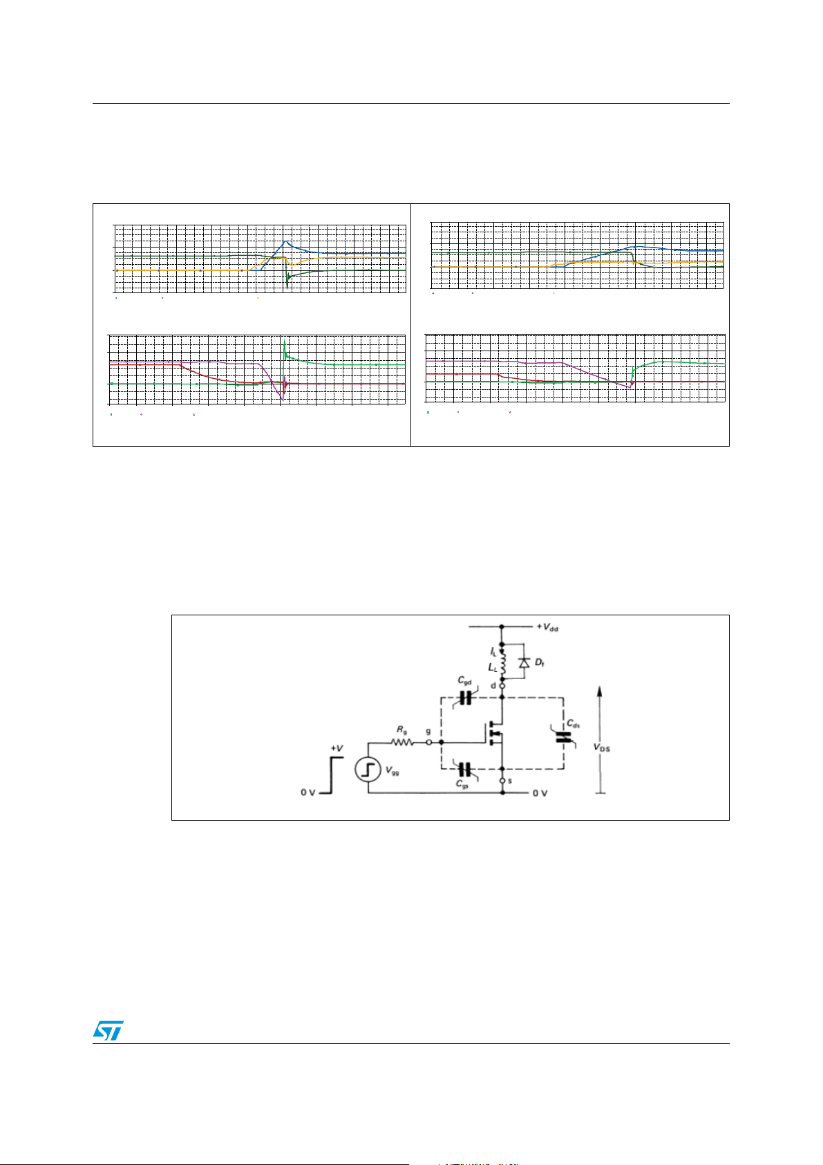
With OrCAD simulations, the principle advantage is the availability of the current waveforms.
It is clear that all the values provided by these simulations are not exact due to real devicePSpice model mismatch.
During the HS turn-on process (Figure 9 and 10, HS V
blue traces, respectively), the inductive load can be modeled as a constant DC current (I
and ID are shown in orange and
GS
,
L
load current) in parallel with the LS body-drain diode. The equivalent circuit is, therefore, a
classic clamped power switching circuit (Figure 9).
Figure 11. Clamped inductive switching circuit
AM07212v1
The drain current rise time, neglecting the parasitic effects caused by the stray inductances,
is given by Equation 2:
Doc ID 17890 Rev 1 11/19
Page 12

Synchronous buck converter testing demonstration board AN3267
¹
©
Equation 2
§
¨
LN#2T
)33'RI
¨
·
66G
4(''FS
¸
¸
)66G
,4(''FS
Varying the gate drive voltage from 5 V to 12 V, using typical power MOSFET electrical
parameters, the normalized power MOSFET rise time is linked to the V
(Figure 12):
GS
Figure 12. Rise time vs. power MOSFET G-S voltage
Normalized rise me vs. V
gs
4.00
3.50
3.00
2.50
2.00
1.50
1.00
0.50
0.00
56789101112
Rise me
Vgs [V]
AM08143v1
Driving the power MOSFET at a lower gate voltage, the device switching speed is
appreciably reduced, while the drain current slope, in HS and LS, becomes less steep, as
clearly shown in Figure 9 and 10. Focusing on the LS device, the current slope (dI
decrease causes reverse recovery time (t
maximum reverse recovery current (I
(Q
) is given, with good approximation, by:
rr
) enlarging and a far more marked reduction of
rr
). The body-drain diode reverse recovery charge
rrm
D,L S
/dt)
Equation 3
≈
0.5 trrI
Q
Q
⋅⋅
rr
values are 20.9 nC (VGS = 5 V) and 34 nC (VGS = 12 V). The stored charge to be
rr
rrm
removed before body diode off-state decreases with the power MOSFET gate drive voltage;
as a consequence, the current stress on the HS device and the phase node spike become
less critical. Referring to Figure 9 and 10, with V
is 14.5 with V
12/19 Doc ID 17890 Rev 1
GS
= 5 V.
= 12 V, V
GS
PHASE,MAX
is 27.1 V whereas, it
Page 13
AN3267 Synchronous buck converter testing demonstration board
3.2 Converter efficiency calculation
The impact of the power MOSFET gate driving voltage on the converter efficiency is
analyzed in this section. As already known, the gate-source voltage controls the power
MOSFET channel, so by increasing the power MOSFET’s V
higher with a lower R
. In other words, driving the power MOSFET gate in the range of
DS(on)
10-12 V optimizes device behavior and efficiency at high currents. In Figure 13, for the
devices mounted on the board, the R
values at different V
DS(on)
, the possible drain current is
GS
are shown.
GS
Figure 13. Impact of V
16
14
12
10
8
6
4
2
0
456789
HS Rdson @ 20 A
At V
= 5 V, the HS and LS on-state resistances are respectively 11.2 mΩ and 4.5 mΩ.
GS
Increasing gate-source voltage up to 12 V, the relative R
improvements with higher V
on power MOSFET R
GS
HS & LS Rdson @ 20 A
LS Rdson @ 20 A
are in the range of [10% - 20%]. Therefore, the conduction
GS
Vgs [V]
DS(on)
10
is 9.9 mΩ and 3.7 mΩ; R
DS(on)
11
(on-state) losses, for the LS device, are given by the following formula:
12
AM08144v1
DS(on
Equation 4
P
COND LS,
The higher the V
1D–()R
⋅⋅=
, the lower the LS conduction losses, maximizing converter efficiency.
GS
DS on()
T() I
For low D values (in this case, D = V
relevant for the whole converter. Higher V
2
DL,
OUT/VIN
= 1.25/12 = 10.4%), this power loss is the most
values also reduce HS conduction losses,
GS
given by:
Equation 5
P
COND HS,
DR
⋅⋅=
DS on()
T() I
2
DHS,
Doc ID 17890 Rev 1 13/19
Page 14

Synchronous buck converter testing demonstration board AN3267
¹
©
Vgs = 5 V
Vgs = 8 V
Vgs = 12 V
Even though this contribution is less important, due to low D values.
Another two power loss contributions linked to the power MOSFET gate-source voltage are
the gate drive power losses (P
) and the HS switching losses. The first are given by:
GATE
Equation 6
P
GATE
N
⋅⋅ ⋅=
FETQgVGGfsw
where:
● N
● Q
● V
● f
is the power MOSFET paralleled number (in HS or LS position)
FET
is the total gate charge
g
is the power MOSFET gate driving voltage
GG
is the switching frequency.
sw
The HS switching losses are:
Equation 7
2
0
§
¨
11
'$'3(337
¨
5004/4
66
0,!4##$26
2
6
0,!4
·
$704/4
¸
¸
F)6
37/54).
where:
● Q
● R
● V
and QGD are the gate-source after the threshold and gate-drain charges
GS2
TOT,P-UP
PLAT
and R
TOT,P-DW
the plateau voltage.
the total HS gate resistance at turn-on and turn-off
Driving the power MOSFETs at 5 V, the gate charge needed to switch the devices on and off
is lower, causing a reduction in P
. Obviously, at low switching frequency this benefit is
GATE
not significant, but becomes important in high frequency converters.
However, the lower the V
is (and therefore HS V
CCDRV
, the higher the P
GS)
SW,HS
is.
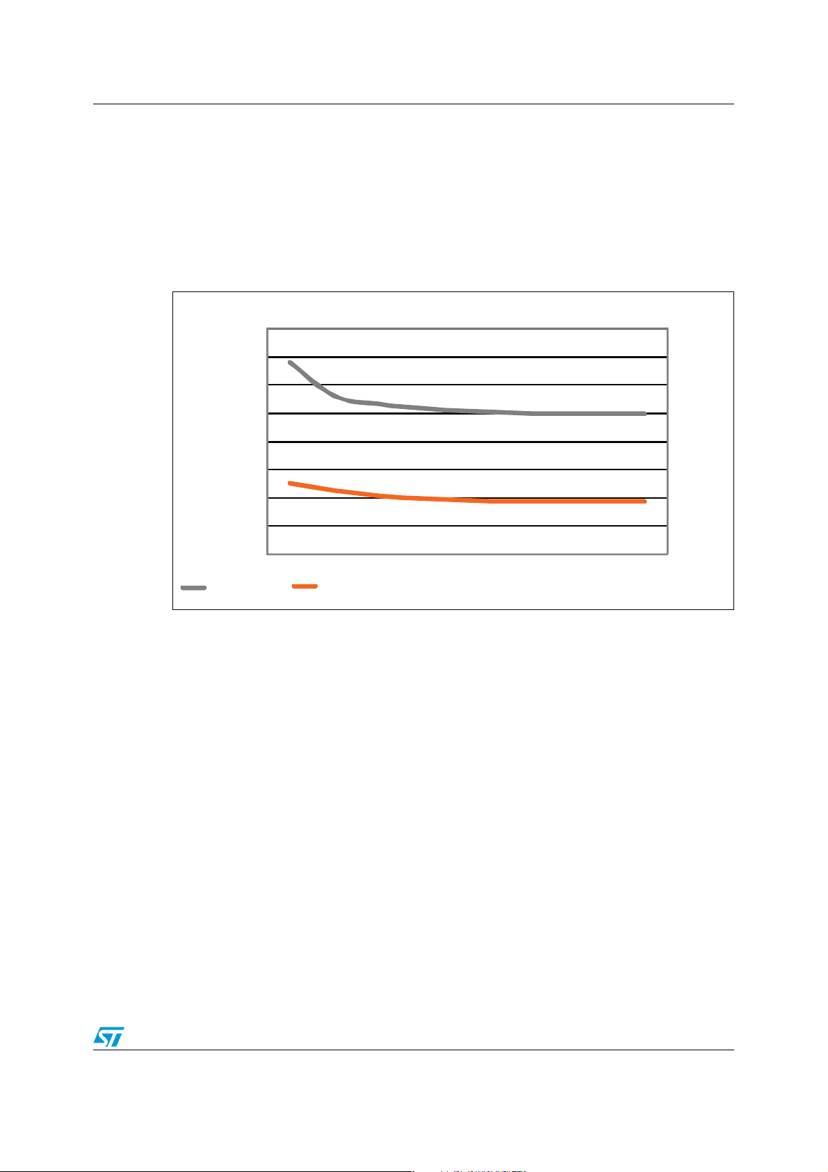
Figure 14. Efficiency comparison
Effici ency comparis on @ Vou t = 1.25 V
88.00
86.00
84.00
82.00
80.00
78.00
76.00
14/19 Doc ID 17890 Rev 1
74.00
2 4 6 8 10 12 14 16 18 20
Iout [A]
AM08145v1
Page 15
AN3267 Synchronous buck converter testing demonstration board
Now, the converter efficiency at three different power MOSFET gate-source voltages
(5 V, 8 V, and 12 V) is calculated, stepping up the load current from 0 to 20 A without airflow.
The curves are shown in Figure 14.
Regarding Figure 14, at low currents the curves are very similar, due to the balance of the
above mentioned loss contributions. Therefore, the V
impact is not evident at light load. At
GS
full load, the gap between 12 V and 5 V curves is conspicuous (2.8% at 20 A), whereas 8 V
and 12 V are very similar both at low and high currents. In fact, according to Figure 11,
R
curve enters “flat zone” for VGS higher than 8 V; consequently, there are no strong
DS(on)
variations in the conduction losses or major power losses at full load.
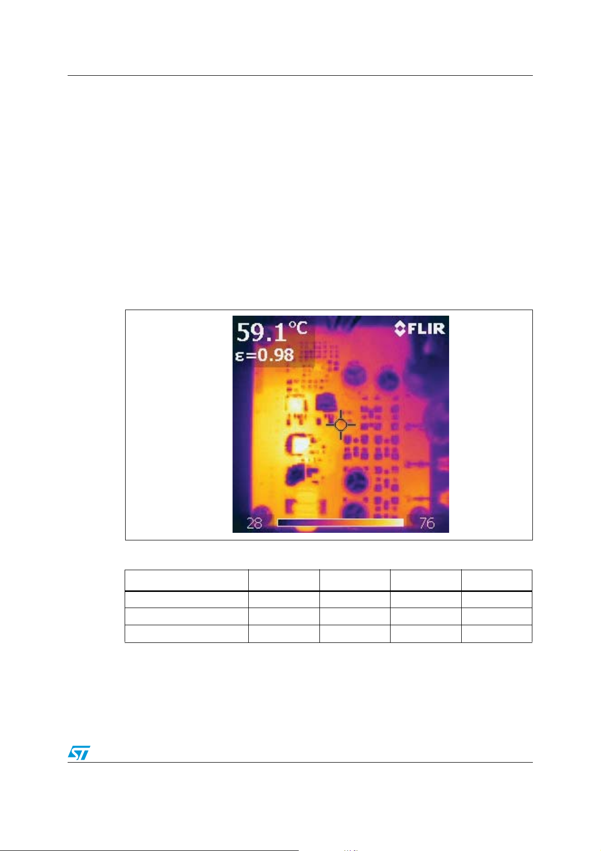
Finally, device temperature at 80% (16 A) of maximum load is measured, after the converter
reaches the thermal equilibrium (around 15-20 min), without airflow. In Figure 15, a thermal
photo captured by a thermo-camera is depicted. In Table 2, the temperature values for the
power MOSFET’s driver and output coil are shown. At V
= 5 V, the power MOSFET’s,
GS
driver and output coil have the hottest temperatures, due to higher losses, while the other
two drive conditions show similar values.
Figure 15. Thermal capture @ 16 A
DRV
HS
LS
Table 2. Temperature measurements @ 16 A
THS (°C) T
V
= 5 V 87.9 69.1 85.2 60.8
GS
= 8 V 77.3 67.1 79 61.4
V
GS
V
= 12 V 75.5 66.3 77.9 61.9
GS
coil
AM08146v1
(°C) TLS (°C) T
DRV
(°C)
Doc ID 17890 Rev 1 15/19
Page 16

Conclusions AN3267
4 Conclusions
Through bench tests and OrCAD simulations, the impact of the power MOSFET gate drive
voltage on device and converter performance has been thoroughly analyzed. In particular,
the MOSFET immunity to high voltage stress on the phase node is higher at low V
(i.e. 5 V). Slowing down the power MOSFET switching speed, the body diode reverse
recovery process is less critical in these operating conditions. On the contrary, the higher
the V
the bigger the reverse recovery charge, causing higher spike on the phase node.
GS
However, when lower voltages are applied to the power MOSFET gate, some power loss
contributions (gate drive, conduction, HS switching losses, etc.) increase, worsening the
overall efficiency. Therefore, the power MOSFET and converter power and thermal
management is optimized at high V
(typically, higher than 8 V), because of the power
GS
MOSFET conduction losses minimization at heavy load conditions.
GS
values
The right V
choice, according to overall system requirements, allows a good trade-off
GS
between phase node spike reduction and efficiency improvement to be reached.
The OrCAD simulations provide a useful tool for understanding and validating the
experimental results. Please consider that the devices’ PSpice models are quite accurate
but not precise, so a mismatch with the experimental results is understandable.
16/19 Doc ID 17890 Rev 1
Page 17

AN3267 References
5 References
1. AN-6005 - Synchronous buck converter losses calculations with Excel model,
J. Klein, Fairchild Semiconductor, 2006
2. L6728 datasheet, STMicroelectronics
3. Power Electronics Handbook
, Muhammad H. Rashid, 2001
Doc ID 17890 Rev 1 17/19
Page 18

Revision history AN3267
6 Revision history
Table 3. Document revision history
Date Revision Changes
25-Aug-2011 1 Initial release.
18/19 Doc ID 17890 Rev 1
Page 19

AN3267
Please Read Carefully:
Information in this document is provided solely in connection with ST products. STMicroelectronics NV and its subsidiaries (“ST”) reserve the
right to make changes, corrections, modifications or improvements, to this document, and the products and services described herein at any
time, without notice.
All ST products are sold pursuant to ST’s terms and conditions of sale.
Purchasers are solely responsible for the choice, selection and use of the ST products and services described herein, and ST assumes no
liability whatsoever relating to the choice, selection or use of the ST products and services described herein.
No license, express or implied, by estoppel or otherwise, to any intellectual property rights is granted under this document. If any part of this
document refers to any third party products or services it shall not be deemed a license grant by ST for the use of such third party products
or services, or any intellectual property contained therein or considered as a warranty covering the use in any manner whatsoever of such
third party products or services or any intellectual property contained therein.
UNLESS OTHERWISE SET FORTH IN ST’S TERMS AND CONDITIONS OF SALE ST DISCLAIMS ANY EXPRESS OR IMPLIED
WARRANTY WITH RESPECT TO THE USE AND/OR SALE OF ST PRODUCTS INCLUDING WITHOUT LIMITATION IMPLIED
WARRANTIES OF MERCHANTABILITY, FITNESS FOR A PARTICULAR PURPOSE (AND THEIR EQUIVALENTS UNDER THE LAWS
OF ANY JURISDICTION), OR INFRINGEMENT OF ANY PATENT, COPYRIGHT OR OTHER INTELLECTUAL PROPERTY RIGHT.
UNLESS EXPRESSLY APPROVED IN WRITING BY TWO AUTHORIZED ST REPRESENTATIVES, ST PRODUCTS ARE NOT
RECOMMENDED, AUTHORIZED OR WARRANTED FOR USE IN MILITARY, AIR CRAFT, SPACE, LIFE SAVING, OR LIFE SUSTAINING
APPLICATIONS, NOR IN PRODUCTS OR SYSTEMS WHERE FAILURE OR MALFUNCTION MAY RESULT IN PERSONAL INJURY,
DEATH, OR SEVERE PROPERTY OR ENVIRONMENTAL DAMAGE. ST PRODUCTS WHICH ARE NOT SPECIFIED AS "AUTOMOTIVE
GRADE" MAY ONLY BE USED IN AUTOMOTIVE APPLICATIONS AT USER’S OWN RISK.
Resale of ST products with provisions different from the statements and/or technical features set forth in this document shall immediately void
any warranty granted by ST for the ST product or service described herein and shall not create or extend in any manner whatsoever, any
liability of ST.
ST and the ST logo are trademarks or registered trademarks of ST in various countries.
Information in this document supersedes and replaces all information previously supplied.
The ST logo is a registered trademark of STMicroelectronics. All other names are the property of their respective owners.
© 2011 STMicroelectronics - All rights reserved
STMicroelectronics group of companies
Australia - Belgium - Brazil - Canada - China - Czech Republic - Finland - France - Germany - Hong Kong - India - Israel - Italy - Japan -
Malaysia - Malta - Morocco - Philippines - Singapore - Spain - Sweden - Switzerland - United Kingdom - United States of America
www.st.com
Doc ID 17890 Rev 1 19/19
 Loading...