

Page 1

AN3261
Application note
Dual push-button Smart Reset™ devices
with user-adjustable setup delays
Introduction
The Smart Reset™ family of devices consists of several products with a combination of
features selected to best suit most typical applications. Their basic common feature is dualbutton reset with setup delay that requires both input reset buttons to be continuously
pressed for a defined period of time. This improves system stability compared to simple
manual reset button devices and eliminates the need for a traditional reset access hole (e.g.
two standard keys on the mobile phone keyboard can be used as Smart Reset™ inputs).
Numerous additional features and device options are factory-programmed or can be
implemented upon request.
Common STM65xx Smart Reset™ family features include:
■ Dual-button Smart Reset™ inputs
■ V
■ Industrial operating temperature range –40 °C to +85 °C
■ Space-saving TDFN8 package (2 mm x 2 mm x 0.75 mm)
■ RoHS compliance
range 1.0 to 5.5 V (active-low output valid)
CC
Differentiating features of the devices are:
■ With or without Power-on Reset (POR)
■ With or without V
■ Independent battery monitoring feature with battery-low warning (STM6505 only)
■ Input logic voltage levels: standard CMOS or fixed threshold
■ Smart Reset™ output characteristics
– Defined reset pulse duration or push-button controlled (undefined) reset pulse
duration
– Reset pulse duration: factory-programmed or capacitor-adjustable
– Smart Reset™ delay: tri-state / dual-state / capacitor-adjustable
– Open-drain or push-pull reset output
– Single or dual reset output
monitoring
CC
September 2010 Doc ID 17837 Rev 1 1/17
www.st.com
Page 2

Contents AN3261
Contents
1 Features . . . . . . . . . . . . . . . . . . . . . . . . . . . . . . . . . . . . . . . . . . . . . . . . . . . 4
2 Typical application diagrams . . . . . . . . . . . . . . . . . . . . . . . . . . . . . . . . . . 5
2.1 Single-button reset . . . . . . . . . . . . . . . . . . . . . . . . . . . . . . . . . . . . . . . . . . . 5
2.2 Dual-button reset . . . . . . . . . . . . . . . . . . . . . . . . . . . . . . . . . . . . . . . . . . . . 7
2.3 Multiple-button reset . . . . . . . . . . . . . . . . . . . . . . . . . . . . . . . . . . . . . . . . . . 8
2.4 Input pull-up considerations (CMOS/fixed levels) . . . . . . . . . . . . . . . . . . . . 9
2.5 Output pull-up considerations . . . . . . . . . . . . . . . . . . . . . . . . . . . . . . . . . . . 9
2.6 Reliability note . . . . . . . . . . . . . . . . . . . . . . . . . . . . . . . . . . . . . . . . . . . . . 10
3 Demonstration boards, promotion tools . . . . . . . . . . . . . . . . . . . . . . . . 11
3.1 STM6503 demonstration board . . . . . . . . . . . . . . . . . . . . . . . . . . . . . . . . 11
3.2 STM65xx interposer boards . . . . . . . . . . . . . . . . . . . . . . . . . . . . . . . . . . . 12
3.3 Smartphone demonstration example . . . . . . . . . . . . . . . . . . . . . . . . . . . . 13
4 Conclusion . . . . . . . . . . . . . . . . . . . . . . . . . . . . . . . . . . . . . . . . . . . . . . . . 15
5 Revision history . . . . . . . . . . . . . . . . . . . . . . . . . . . . . . . . . . . . . . . . . . . 16
2/17 Doc ID 17837 Rev 1
Page 3

AN3261 List of figures
List of figures
Figure 1. Single-button Smart Reset™ typical application diagram, with “early-warning”
feature, STM6503 . . . . . . . . . . . . . . . . . . . . . . . . . . . . . . . . . . . . . . . . . . . . . . . . . . . . . . . . . 5
Figure 2. Timing diagram - single push-button Smart Reset™ . . . . . . . . . . . . . . . . . . . . . . . . . . . . . . 6
Figure 3. Dual push-button Smart Reset™ typical application diagram, STM6503 . . . . . . . . . . . . . . . 7
Figure 4. Timing diagram - dual push-button Smart Reset™. . . . . . . . . . . . . . . . . . . . . . . . . . . . . . . . 7
Figure 5. Three push-button delayed Smart Reset™ typical application diagram, STM6503 . . . . . . . 8
Figure 6. Timing diagram - three push-button Smart Reset™ . . . . . . . . . . . . . . . . . . . . . . . . . . . . . . . 9
Figure 7. Smart Reset™ demonstration board, STM6503. . . . . . . . . . . . . . . . . . . . . . . . . . . . . . . . . 11
Figure 8. The STM65xx interposer boards; a dedicated board is available for each STM65xx
Smart Reset™ device . . . . . . . . . . . . . . . . . . . . . . . . . . . . . . . . . . . . . . . . . . . . . . . . . . . . . 12
Figure 9. Smartphone demonstration example shows STM6503 implemented in an actual
application. . . . . . . . . . . . . . . . . . . . . . . . . . . . . . . . . . . . . . . . . . . . . . . . . . . . . . . . . . . . . . 13
Figure 10. Smart Reset™ demonstration in an actual smartphone application. . . . . . . . . . . . . . . . . . 14
Doc ID 17837 Rev 1 3/17
Page 4

Features AN3261
1 Features
● The Smart Reset™ functionality is a feature that introduces a reset output response
delay. Both of the Smart Reset™ input buttons must be pressed for a defined t
period, only after which an output reset pulse is generated. This results in a robust
hardware reset. The reset function can then be assigned to the existing keys of a
device, which eliminates the traditional reset hole in the back cover of the device, while
maintaining system stability. All the STM65xx family devices have this feature with the
exception of the STM6504.
● The edge trigger functionality is a reset input with an immediate reset response and a
special debounce feature. Found only on the STM6504 (a device with single-button
edge trigger immediate reset and a single-button delayed Smart Reset™ input,
independent but with a common reset output).
● V
● Battery-low detection is an additional independent voltage monitoring function with a
monitoring/undervoltage reset. When the monitored VCC voltage drops below
CC
the factory-programmed undervoltage reset threshold V
immediately go active and remain so until V
the defined t
REC
period.
rises above V
CC
, the reset output(s)
RST
and hysteresis, plus
RST
dedicated battery-low detection output pin. It works as a pure comparator with
V
=1.25 V. STM6505 only.
REF
● Fixed input logic levels are suitable for configurations where the device driving the
input buttons (keyboard) is connected to a lower voltage than the supply voltage of the
STM65xx device. This is in contrast to the devices with the standard CMOS input logic
levels that are relative to V
and are suitable only for applications in which the device
CC
driving the inputs of the Smart Reset™ device is powered by the same voltage supply.
SRC
4/17 Doc ID 17837 Rev 1
Page 5
AN3261 Typical application diagrams
2 Typical application diagrams
The STM65xx family of Smart Reset™ products provides a broad variety of options for
various types of applications.
2.1 Single-button reset
The STM65xx devices allow for different reset input configurations. In simple applications,
only one input reset button with delayed reset may be sufficient. In this case, for product
options without internal input pull-up resistors, SR0
together or the unused SR
input permanently grounded. In the case of a product version
with internal input pull-up resistors, just connect the inputs together. Permanent grounding
of the unused SR
pull-up resistor from V
input would, in this case, cause a continuous current to flow through the
to VSS.
CC
Figure 1. Single-button Smart Reset™ typical application diagram, with “early-
warning” feature, STM6503
V
CC
and SR1 can be either connected
V
CC
RST
TSR
RESET
STM6503
SR1
Early
V
1. Early warning feature: the input reset push-button can be also used as an early warning to the processor
(through the interrupt input) that a reset may come after the t
SR0
SS
warning
SRC
INT/
NMI
reset setup delay.
V
CC
MCU
V
SS
PUSH-BUTTON
SWITCH
Doc ID 17837 Rev 1 5/17
Page 6
Typical application diagrams AN3261
Figure 2. Timing diagram - single push-button Smart Reset™
t
SRC
SR0
SR1
t
REC
RST
6/17 Doc ID 17837 Rev 1
Page 7

AN3261 Typical application diagrams
2.2 Dual-button reset
The most frequent application requires a configuration with two reset buttons which further
improves immunity to undesired resets by adding a second input reset button with delayed
reset. In this case, the reset pulse occurs only when both the buttons have been pressed
and held for the defined t
Figure 3. Dual push-button Smart Reset™ typical application diagram, STM6503
V
CC
SRC
delay.
V
CC
RST
TSR
RESET
STM6503
SR1
INT/
NMI
SS
SR0
PUSH-BUTTON
SWITCH
PUSH-BUTTON
SWITCH
V
Figure 4. Timing diagram - dual push-button Smart Reset™
t
SRC
V
CC
MCU
V
SS
SR0
SR1
RST
t
REC
Doc ID 17837 Rev 1 7/17
Page 8
Typical application diagrams AN3261
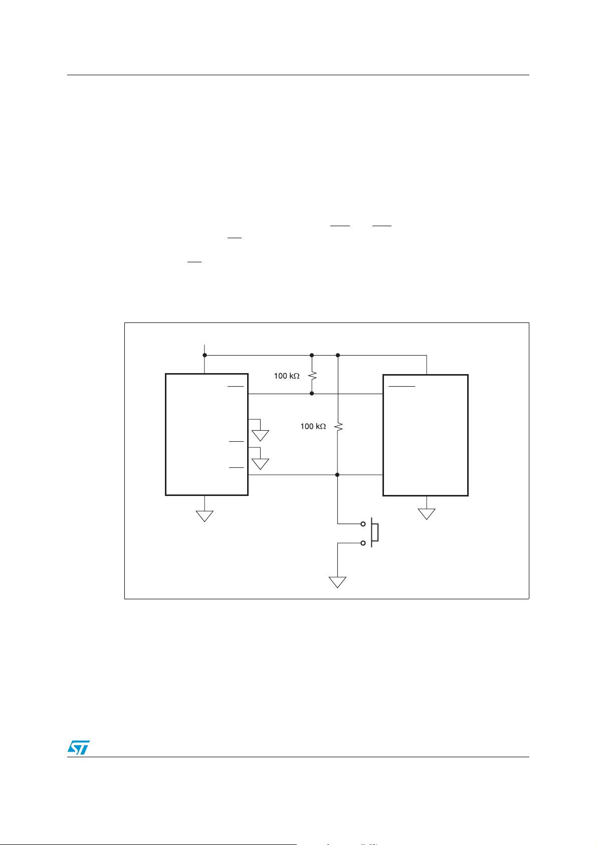
2.3 Multiple-button reset
Adding even more input buttons is possible by adding a simple OR gate. All of the buttons
must then be pressed simultaneously for at least t
pulse on the STM65xx output. For a configuration with three input reset buttons, connect
one button to one SR
output to the second SR
input as usual and the remaining two buttons to an OR gate and tie its
input.
Figure 5. Three push-button delayed Smart Reset™ typical application diagram,
STM6503
input delay seconds to get a reset
SRC
V
CC
100 kΩ 100 kΩ
100 kΩ
OR gate
SR0
SR1
STM65xx
8/17 Doc ID 17837 Rev 1
Page 9

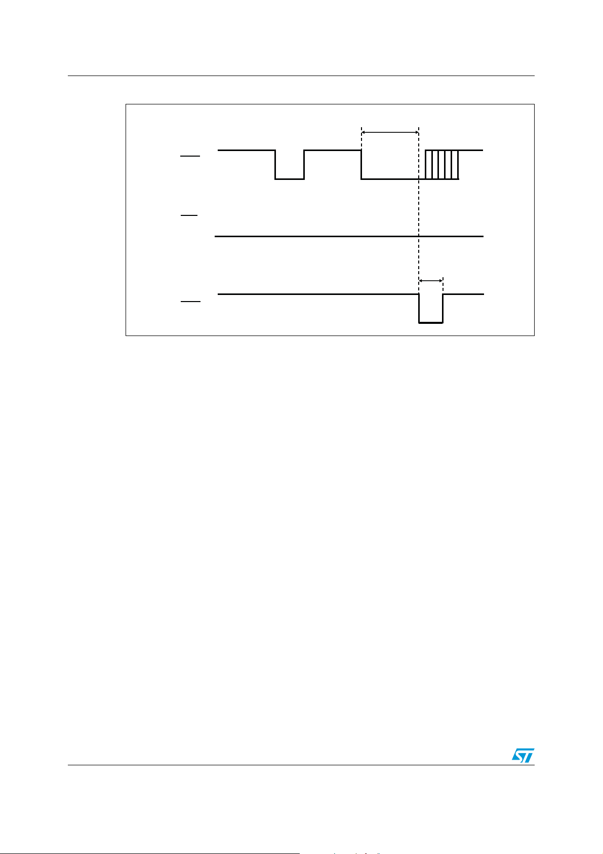
AN3261 Typical application diagrams
Figure 6. Timing diagram - three push-button Smart Reset™
t
SRC
Push-
button 1
Push-
button 2
Push-
button 3
t
REC
RST
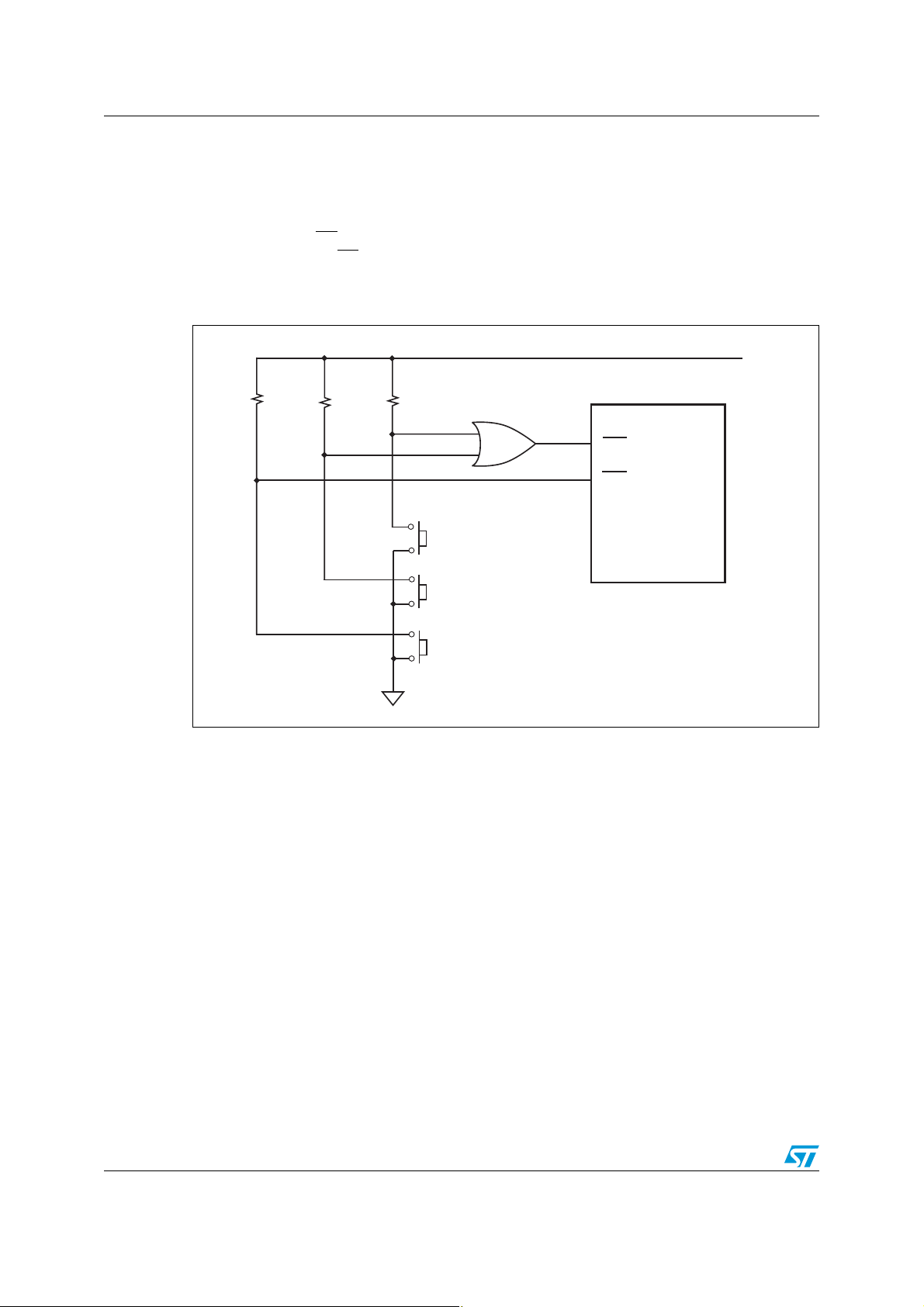
2.4 Input pull-up considerations (CMOS/fixed levels)
Inputs without internal pull-up resistors can be pulled to a different voltage level than the
supply voltage of the STM65xx devices, however:
● the input pull-up voltage level should not exceed 5.5 V
● the input logic levels specifications must be respected:
–V
–V
min = 0.7VCC, VILmax = 0.3VCC in case of standard CMOS input cells (it is
IH
recommended to always keep V
min = 0.85 V, VILmax = 0.3 V in case of the fixed-logic levels devices
IH
on the ground level and VIH on the VCC level)
IL
(STM6520, STM6522).
2.5 Output pull-up considerations
Open-drain RST outputs without internal pull-up resistors can also be pulled up to any
voltage independent of V
be respected). The STM65xx devices can thus serve also as a simple level shifter.
(higher or lower than VCC) (but absolute maximum ratings must
CC
Doc ID 17837 Rev 1 9/17
Page 10

Typical application diagrams AN3261
2.6 Reliability note
Devices with timings adjusted by external components vs. environmental
considerations
For device options with timings (t
SRC
, t
) adjusted by an external capacitor, there are
REC
several additional factors to be considered that may affect the accuracy of the timings. The
given specifications apply to the STM65xx device alone, i.e. with an ideal timing capacitor.
External tolerances, temperature dependencies and leakages are excluded.
The Smart Reset™ devices are designed to meet strict requirements for the lowest possible
current consumption and to maintain the common timing constant 10 s/µF, therefore the
constant current used to charge the external timing capacitor is very low, in the magnitude of
100 nA. Any external leakage (e.g. poor quality timing capacitors or excessive humidity,
especially if dew-point is exceeded and moisture condensation occurs on the PCB tracks)
may cause a significant leakage current which is deducted from the constant charging
current that the device provides, reducing the effective external timing capacitor charging
current which results in extending the t
tracks between the SRC (TREC
) pin and its respective timing capacitor should be as
ADJ
SRC
(t
) timings. To minimize this effect, the PCB
REC
short as possible, properly covered with solder mask and isolated from other tracks
(especially V
) by as great a distance as possible. Also, low-leakage timing capacitors
SS
(ceramic or film capacitor) should be used.
10/17 Doc ID 17837 Rev 1
Page 11

AN3261 Demonstration boards, promotion tools
3 Demonstration boards, promotion tools
A complete set of demonstration/promotion tools is available for various purposes, from
easy, high-level application functional demonstration, down to tools for detailed testing.
These tools are based on the STM6503 as the primary representative of the Smart Reset™
family, as the basic Smart Reset™ functionality is common.
3.1 STM6503 demonstration board
Purpose
The demonstration board serves as a functional demonstration of the Smart Reset™
devices and the easily accessible test points provide for basic measurements and testing.
Figure 7. Smart Reset™ demonstration board, STM6503
● Simultaneous push of the SR0 and SR1 buttons is indicated by an LED
● LED and audible indication of the reset pulse after t
● Test points available for easy tracking of the Smart Reset™ signals
● Jumper-selectable Smart Reset™ delay (2/6/10 seconds minimum)
Doc ID 17837 Rev 1 11/17
reset delay
SRC
Page 12
Demonstration boards, promotion tools AN3261
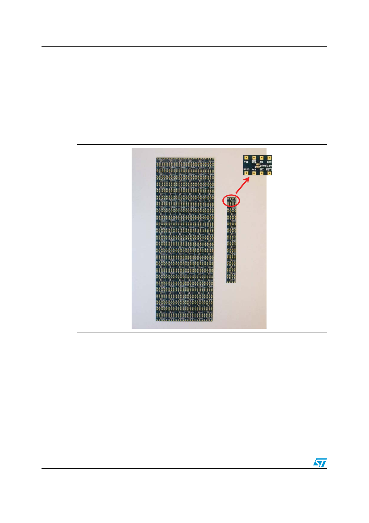
3.2 STM65xx interposer boards
Purpose
The dedicated interposer PC boards were created for each STM65xx Smart Reset™ device
for a quick and flexible application/testing setup preparation. The boards include labels on
each pin for easy identification. The pitch of the interposer pins easily fits into a breadboard
and allows a very flexible application setup testing, or soldering wires for external
connections (to a tester for example).
Figure 8. The STM65xx interposer boards; a dedicated board is available for each
STM65xx Smart Reset™ device
12/17 Doc ID 17837 Rev 1
Page 13
AN3261 Demonstration boards, promotion tools
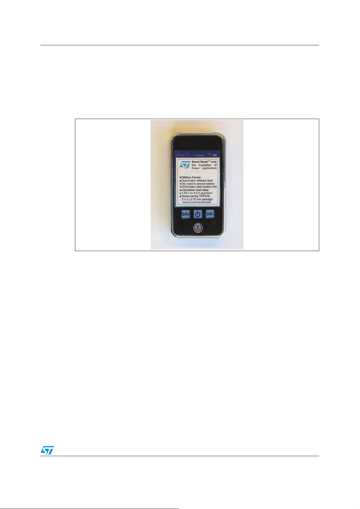
3.3 Smartphone demonstration example
Purpose
The STM65xx smartphone demonstration shows the Smart Reset™ concept and
functionality in a real application (dual push-button delayed reset):
Figure 9. Smartphone demonstration example shows STM6503 implemented in an
actual application
Doc ID 17837 Rev 1 13/17
Page 14

Demonstration boards, promotion tools AN3261
Smart Reset™ concept demonstration
● Push ON/OFF button → goes into a normal ON state (amber display backlight on)
● Push stuck button → goes into stuck mode that simulates frozen smartphone (red
display backlight on) during which it cannot even be turned off
● Push SR0 and SR1 buttons simultaneously for 2 (6 or 10) seconds minimum (jumper-
selectable) → returns to the normal state from which it can be turned off by pressing
the ON/OFF button
Figure 10. Smart Reset™ demonstration in an actual smartphone application
14/17 Doc ID 17837 Rev 1
Page 15

AN3261 Conclusion
4 Conclusion
The family of Smart Reset™ devices provides a variety of smartphone or PDA hardware
reset solutions, some examples of which are shown in this application note, others are in the
datasheet of the specific device. The most up-to-date information on the Smart Reset™
portfolio can be found at www.st.com/smartreset.
Doc ID 17837 Rev 1 15/17
Page 16

Revision history AN3261
5 Revision history
Table 1. Document revision history
Date Revision Changes
22-Sep-2010 1 Initial release.
16/17 Doc ID 17837 Rev 1
Page 17

AN3261
Please Read Carefully:
Information in this document is provided solely in connection with ST products. STMicroelectronics NV and its subsidiaries (“ST”) reserve the
right to make changes, corrections, modifications or improvements, to this document, and the products and services described herein at any
time, without notice.
All ST products are sold pursuant to ST’s terms and conditions of sale.
Purchasers are solely responsible for the choice, selection and use of the ST products and services described herein, and ST assumes no
liability whatsoever relating to the choice, selection or use of the ST products and services described herein.
No license, express or implied, by estoppel or otherwise, to any intellectual property rights is granted under this document. If any part of this
document refers to any third party products or services it shall not be deemed a license grant by ST for the use of such third party products
or services, or any intellectual property contained therein or considered as a warranty covering the use in any manner whatsoever of such
third party products or services or any intellectual property contained therein.
UNLESS OTHERWISE SET FORTH IN ST’S TERMS AND CONDITIONS OF SALE ST DISCLAIMS ANY EXPRESS OR IMPLIED
WARRANTY WITH RESPECT TO THE USE AND/OR SALE OF ST PRODUCTS INCLUDING WITHOUT LIMITATION IMPLIED
WARRANTIES OF MERCHANTABILITY, FITNESS FOR A PARTICULAR PURPOSE (AND THEIR EQUIVALENTS UNDER THE LAWS
OF ANY JURISDICTION), OR INFRINGEMENT OF ANY PATENT, COPYRIGHT OR OTHER INTELLECTUAL PROPERTY RIGHT.
UNLESS EXPRESSLY APPROVED IN WRITING BY AN AUTHORIZED ST REPRESENTATIVE, ST PRODUCTS ARE NOT
RECOMMENDED, AUTHORIZED OR WARRANTED FOR USE IN MILITARY, AIR CRAFT, SPACE, LIFE SAVING, OR LIFE SUSTAINING
APPLICATIONS, NOR IN PRODUCTS OR SYSTEMS WHERE FAILURE OR MALFUNCTION MAY RESULT IN PERSONAL INJURY,
DEATH, OR SEVERE PROPERTY OR ENVIRONMENTAL DAMAGE. ST PRODUCTS WHICH ARE NOT SPECIFIED AS "AUTOMOTIVE
GRADE" MAY ONLY BE USED IN AUTOMOTIVE APPLICATIONS AT USER’S OWN RISK.
Resale of ST products with provisions different from the statements and/or technical features set forth in this document shall immediately void
any warranty granted by ST for the ST product or service described herein and shall not create or extend in any manner whatsoever, any
liability of ST.
ST and the ST logo are trademarks or registered trademarks of ST in various countries.
Information in this document supersedes and replaces all information previously supplied.
The ST logo is a registered trademark of STMicroelectronics. All other names are the property of their respective owners.
© 2010 STMicroelectronics - All rights reserved
STMicroelectronics group of companies
Australia - Belgium - Brazil - Canada - China - Czech Republic - Finland - France - Germany - Hong Kong - India - Israel - Italy - Japan -
Malaysia - Malta - Morocco - Philippines - Singapore - Spain - Sweden - Switzerland - United Kingdom - United States of America
www.st.com
Doc ID 17837 Rev 1 17/17
 Loading...