

Page 1
Multi-bank reference design description and settings
1 Introduction
The M24LR64-R multi-bank reference design has been created to help users increase the
memory density of their Dual Interface EEPROM, and has been designed in a way that will
minimize the antenna size and the I²C interface footprint on the PCB.
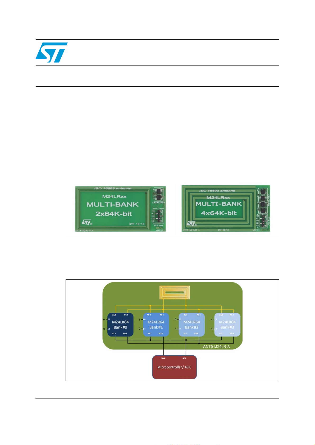
STMicroelectronics has prepared two reference designs:
● ANT4-M24LR-A is a 2-bank reference design with a 128-Kbit EEPROM user memory
● ANT5-M24LR-A is a 4-bank reference design with a 256-Kbit EEPROM user memory
Figure 1. ANT4-M24LR-A design Figure 2. ANT5-M24LR-A design
AN3250
Application note
M24LR64-R
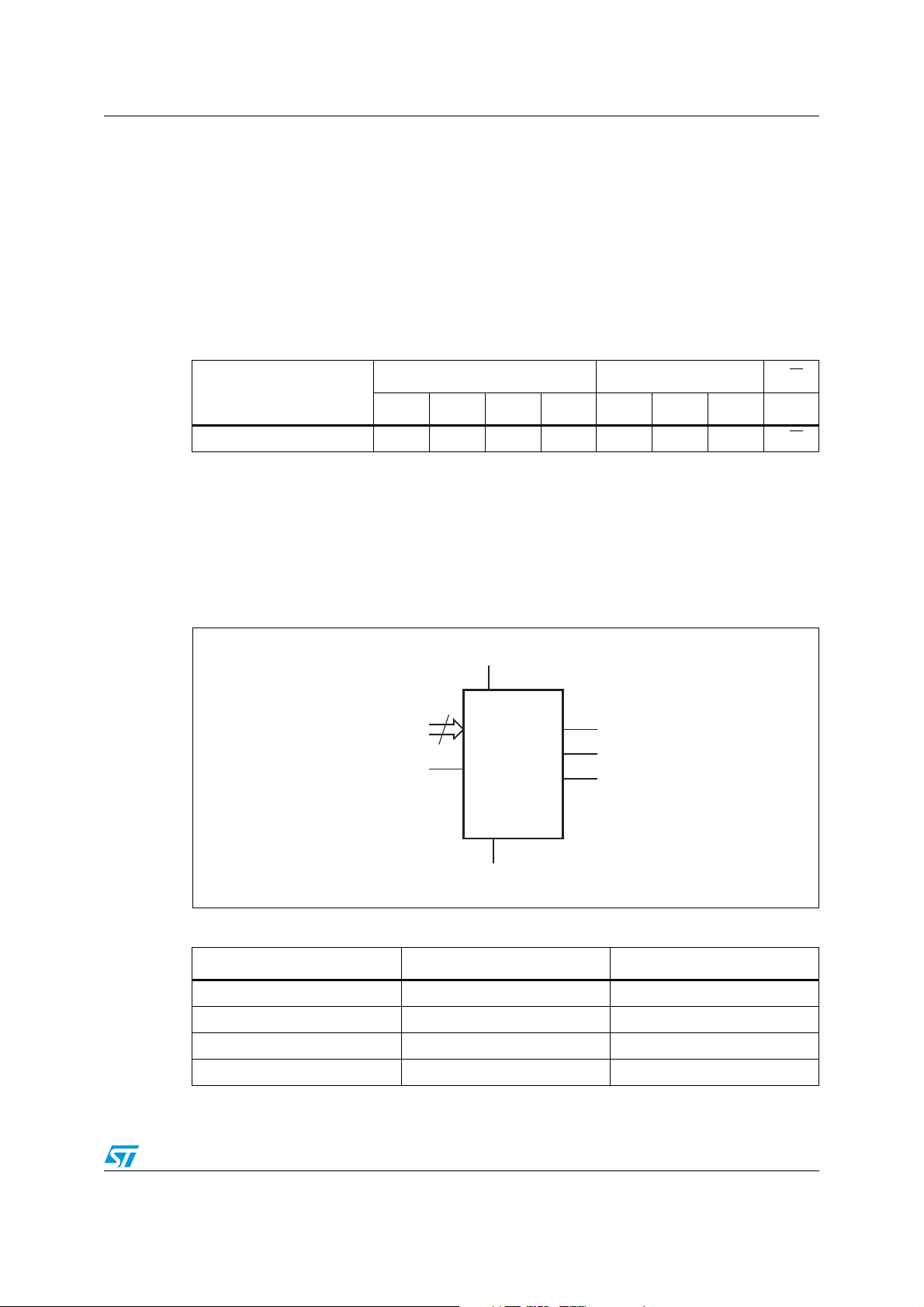
The basic principle is to connect several M24LR64-R devices in parallel on the same I²C bus
(in compliance with I²C specifications) and for them to share one single antenna.
This application note describes how the M24LR64-R Multi-Bank reference design works
from the schematics and design perspective, and explains how to configure and use it.
Figure 3. Design overview
July 2010 Doc ID 17761 Rev 1 1/16
www.st.com
Page 2

Contents AN3250
Contents
1 Introduction . . . . . . . . . . . . . . . . . . . . . . . . . . . . . . . . . . . . . . . . . . . . . . . . 1
2 Designing an M24LR64-R multi-bank application . . . . . . . . . . . . . . . . . 3
2.1 Accessing several EEPROMs on the same I2C bus . . . . . . . . . . . . . . . . . 3
2.2 Connecting several M24LR64-R devices on the same inductive antenna . 5
3 Setting up a Multi-Bank application . . . . . . . . . . . . . . . . . . . . . . . . . . . . 8
3.1 Basic principle . . . . . . . . . . . . . . . . . . . . . . . . . . . . . . . . . . . . . . . . . . . . . . 8
3.1.1 Microcontroller's perspective . . . . . . . . . . . . . . . . . . . . . . . . . . . . . . . . . . 9
3.1.2 RF reader's perspective . . . . . . . . . . . . . . . . . . . . . . . . . . . . . . . . . . . . . 10
3.1.3 Overall perspective . . . . . . . . . . . . . . . . . . . . . . . . . . . . . . . . . . . . . . . . 11
3.2 Setting up the Multi-Bank design . . . . . . . . . . . . . . . . . . . . . . . . . . . . . . . 12
3.2.1 Microcontroller only is available during setup . . . . . . . . . . . . . . . . . . . . 12
3.2.2 RFID reader only is available during setup . . . . . . . . . . . . . . . . . . . . . . 13
3.2.3 Both Microcontroller and RFID reader are available during setup . . . . . 14
4 Conclusion . . . . . . . . . . . . . . . . . . . . . . . . . . . . . . . . . . . . . . . . . . . . . . . . 15
5 Revision history . . . . . . . . . . . . . . . . . . . . . . . . . . . . . . . . . . . . . . . . . . . 15
2/16 Doc ID 17761 Rev 1
Page 3
AN3250 Designing an M24LR64-R multi-bank application
AI15106b
2
E0-E1 SDA
V
CC
M24LR64-R
SCL
V
SS
AC0
AC1
2 Designing an M24LR64-R multi-bank application
2.1 Accessing several EEPROMs on the same I2C bus
The I2C specification allows the use of several devices on the same I2C bus, and this
reference design follows this specification. Please refer to the I
2
C specification and to the
M24LR64-R datasheet for more details.
Each device is accessed according to its value defined by the Device Select code.
Table 1. Device Select code description
Device type identifier
(1)
Chip Enable address
(2)
RW
b7 b6 b5 b4 b3 b2 b1 b0
(3)
Device Select code 1010E2
1. The most significant bit (b7) is sent first.
2. E0 and E1 are compared against the respective external pins on the memory device.
3. E2 is not connected to any external pin. It is however used to address the M24LR64-R system area as
described in the datasheet.
E1 E0 RW
The M24LR64-R offers two Chip Enable pins, E0 and E1. These signals are used to set the
values that are to be looked for on bits b2 and b1 of the 7-bit Device Select code.
Figure 4. Logic diagram
Table 2. Signal descriptions
Signal name Function Direction
E0, E1 Chip Enable Input
SDA Serial Data I/O
SCL Serial Clock Input
AC0, AC1 Antenna coils I/O
Doc ID 17761 Rev 1 3/16
Page 4
Designing an M24LR64-R multi-bank application AN3250
Ai12807a
V
CC
M24LR64
V
SS
E1
E0
0
V
CC
M24LR64
V
SS
E1
E0
1
V
CC
M24LR64
V
SS
E1
E0
2
V
CC
M24LR64
V
SS
E1
E0
3
I2C Bus
Table 2. Signal descriptions (continued)
Signal name Function Direction
V
CC
V
SS
Supply voltage
Ground
E0 and E1 inputs must be tied to VCC (‘1’) or VSS (‘0’) to establish the Device Select code.
When not connected (left floating), these inputs are read as low (‘0’). Using bits E0 and E1
of the Device Select code, up to four M24LR64-R devices can be accessed on the same I
2
bus. This enables emulation of up to 256 Kbits of EEPROM.
In the configuration example shown in Figure 5, in order to access 256 Kbits of EEPROM,
four 64-Kbit M24LR64-R devices are connected to the same I
signals of each device are assigned in a way to create an unique I
2
C bus and the E0 and E1
2
C address for each
specific device.
Figure 5. Configuration example
C
M24LR64-R #0 (Bank 0)
Device addressed as (0,0): pin E0 connected to VSS and pin E1 connected to VSS.
Device type identifier Chip Enable address RW
b7 b6 b5 b4 b3 b2 b1 b0
Device Select code 1010E200RW
M24LR64-R #1 (Bank 1)
Device addressed as (0,1): pin E0 connected to VCC and pin E1 connected to VSS.
Device type identifier Chip Enable address RW
b7 b6 b5 b4 b3 b2 b1 b0
Device Select code 1010E201RW
4/16 Doc ID 17761 Rev 1
Page 5

AN3250 Designing an M24LR64-R multi-bank application
f
TUNING
1
2Π L
INDUCTORCTUNINGIC
••
----------------------------------------------------------------------------------- -=
M24LR64-R #2 (Bank 2)
Device addressed as (1,0): pin E0 connected to VSS and pin E1 connected to VCC.
Device type identifier Chip Enable address RW
b7 b6 b5 b4 b3 b2 b1 b0
Device Select code 1010E210RW
M24LR64-R #3 (Bank 3)
Device addressed as (1,1): pin E0 connected to VCC and pin E1 connected to VCC.
Device type identifier Chip Enable address RW
b7 b6 b5 b4 b3 b2 b1 b0
Device Select code 1010E211RW
To emulate a 256-Kbit device using four M24LR64-R devices, the 256 Kbits are dispatched
as follows:
● M24LR64 #0 will store the 1st block of 64-Kbit EEPROM memory area.
● M24LR64 #1 will store the 2nd block of 64-Kbit EEPROM memory area.
● M24LR64 #2 will store the 3rd block of 64-Kbit EEPROM memory area.
● M24LR64 #3 will store the 4th block of 64-Kbit EEPROM memory area.
2.2 Connecting several M24LR64-R devices on the same inductive antenna
The RF interface of M24LR64 devices is based on a passive RFID technology operating at
13.56 MHz in compliance with ISO/IEC 15693 standards. The basic principles of this RF
technology and antenna design considerations are described in the following two application
notes:
● AN2972: Designing an antenna for the M24LR64-R dual interface I²C/RFID device
● AN3178: Using a surface mount inductor as an M24LRxx antenna
The basic principle of the M24LR64-R's antenna is very simple; the external antenna
inductance (L
INDUCTOR
internal tuning capacitance (C
MHz. This is because ISO/IEC 15693 RFID readers operate in the 13.56 MHz high
frequency band.
In this reference design, we connect a number n of M24LR64-R devices in parallel on the
same antenna. The resulting equivalent tuning capacitance (C
the tuning capacitance of a single M24LR64-R.
) that must be integrated on the PCB should match the M24LRxx's
TUNING_IC
C
TUNING_MULTI-BANK
) in order to create a circuit resonating at 13.56
TUNING_MULTI-BANK
= n x C
TUNING_IC
) is n times
Doc ID 17761 Rev 1 5/16
Page 6

Designing an M24LR64-R multi-bank application AN3250
As the antenna tuning frequency (f
TUNING
) must remain at 13.56 MHz, designers must
decrease the antenna inductance by the same factor as the increase of the tuning
capacitance of a multi-bank circuit:
L
MULTI_BANK
= L
INDUCTOR
/ n
In the following example, four M24LR64-R devices are connected in parallel on the same
antenna. The inductance value of this antenna must be four times smaller than the one used
for a single M24LR64-R.
As a reference, Figure 6 represents a single antenna single M24LR64-R device as per
STMicroelectronics ANT1-M24LR-A reference design.
Figure 6. Block diagram for ANT1-M24LR-A reference design
The ANT5-M24LR-A reference design (Figure 7) consists of four M24LR64-R devices in
parallel, resulting in 256 Kbits of equivalent user memory. The equivalent tuning capacitance
value is 4 times that of a single M24LR64-R device. So the antenna, whether it is designed
on a PCB or uses an SMD inductor, must be 4 times smaller than the one used for one
single M24LR64-R device.
6/16 Doc ID 17761 Rev 1
Page 7

AN3250 Designing an M24LR64-R multi-bank application
Figure 7. Block diagram for ANT5-M24LR-A reference design
IMPORTANT: As per application notes AN2972 and AN3178, ST recommends antenna
designers to prototype different types of antennas with different inductance values in order
to select the antenna that will give the best results in their application.
Doc ID 17761 Rev 1 7/16
Page 8

Setting up a Multi-Bank application AN3250
3 Setting up a Multi-Bank application
Once designed, the Multi-Bank application must be configured and programmed so that it
can be used correctly by the microcontroller and the RFID reader. Because several banks
are used in parallel, each bank must be individually numbered and this number must be
common to both the RFID reader and the microcontroller.
This reference design proposes to identify the banks and their numbers using a pointer area
placed at the end of the last bank of the reference design.
There are different ways to allocate the banks depending on whether a microcontroller only,
an RFID reader only or both a microcontroller and an RFID reader are available in the
application during Multi-Bank programming.
For further details on how the M24LR64-R arbitration unit operates, refer to application note
AN3057 “How to manage M24LR64-R data transfers from the I²C bus or an RF channel”.
While the 3 following setup methods work, the one with both a microcontroller and RFID
reader is recommend as it speeds up the identification process when the application is
running.
3.1 Basic principle
Each memory bank of the Multi-Bank reference design consists of an M24LR64-R memory
plan which includes among others:
● A 64-bit Unique IDentifier area (UID)
– Read-only in RF mode
– Read-only in I
● An 8-bit Data Storage IDentifier area (DSFID)
– Read-write in RF mode
– Read-only in I
● A 64-Kbit EEPROM user memory area
– Read-write in RF mode
– Read-write in I
Note: This application note illustrates the setup of the ANT5-M24LR-A, which is the 4-bank
reference design. The same principle applies for any Multi-Bank design.
2
C mode
2
C mode
2
C mode
8/16 Doc ID 17761 Rev 1
Page 9

AN3250 Setting up a Multi-Bank application
Ai18131
UID 0 UID 1 UID 2 UID 3
DSFID DSFID DSFID DSFID
Bank 0 Bank 1 Bank 2 Bank 3
E0 = 0
E1 = 0
E0 = 1
E1 = 0
E0 = 0
E1 = 1
E0 = 1
E1 = 1
Microcontroller or ASIC
3.1.1 Microcontroller's perspective
From the microcontroller's perspective, each bank is addressed using E0 and E1 pins, as
shown in Figure 8.
Figure 8. Addressing the 4 banks with a microcontroller (I²C only)
Doc ID 17761 Rev 1 9/16
Page 10

Setting up a Multi-Bank application AN3250
Ai18130
UID 0 UID 1 UID 2 UID 3
DSFID DSFID DSFID DSFID
Bank 0 Bank 1 Bank 2 Bank 3
3.1.2 RF reader's perspective
From the RFID reader perspective, each bank is identified by its UID, which is accessible
during the basic inventory round. UIDs are used for addressing each device as shown in
Figure 9.
Figure 9. Addressing the 4 banks in RF mode (with UID)
10/16 Doc ID 17761 Rev 1
Page 11

AN3250 Setting up a Multi-Bank application
Ai18132
UID UID UID UID
DSFID DSFID DSFID DSFID
Bank 0 Bank 1 Bank 2 Bank 3
UID0 (E0 = 0, E1 = 0)
UID1 (E0 = 1, E1 = 0)
UID2 (E0 = 0, E1 = 1)
UID3 (E0 = 1, E1 = 1)
E0E1/UID
Mapping
area
3.1.3 Overall perspective
If both the Microcontroller and the RFID reader need to share the same bank numbering
scheme, both E0 E1 values (for addressing each bank by the Microcontroller) and UID
values (for addressing each bank by the RFID reader) must be mapped.
This is performed by storing the UID of the corresponding E0E1 signals at the end of the last
memory bank as shown in Figure 10.
Figure 10.
Doc ID 17761 Rev 1 11/16
Page 12

Setting up a Multi-Bank application AN3250
Ai18134
UID UID UID UID
DSFID DSFID DSFID DSFID
Bank Bank Bank Bank
E0 = 0, E1 = 0
( = Bank 0)
E0 = 1, E1 = 0
( = Bank 1)
E0 = 0, E1 = 1
( = Bank 2)
E0 = 1, E1 = 1
( = Bank 3)
Microcontroller or ASIC
UID0 (E0 = 0, E1 = 0)
UID1 (E0 = 1, E1 = 0)
UID2 (E0 = 0, E1 = 1)
UID3 (E0 = 1, E1 = 1)
E0E1/UID
Mapping
area
3.2 Setting up the Multi-Bank design
When setting up a multi-bank design, there are different ways to allocate (identify) the banks
depending on whether a microcontroller only, an RFID reader only or both a microcontroller
and an RFID reader are available during Multi-Bank programming.
3.2.1 Microcontroller only is available during setup
When only the microcontroller (I²C only) is available to program the Multi-Bank setting
information, it addresses each M24LR64-R device separately and stores the corresponding
UID in its volatile memory.
Figure 11.
Once the UIDs of the 4 devices are read, the Microcontroller programs the 4 UIDs at the end
of Bank #3, which is addressed with E0=E1=1.
● Program UID of Bank (E0=0, E1=0) at address 0x07F8 and 0x07F9
● Program UID of Bank (E0=1, E1=0) at address 0x07FA and 0x07FB
● Program UID of Bank (E0=0, E1=1) at address 0x07FC and 0x07FD
12/16 Doc ID 17761 Rev 1
● Program UID of Bank (E0=1, E1=1) at address 0x07FE and 0x07FF
Page 13

AN3250 Setting up a Multi-Bank application
At this time, the only way for the RFID reader to correctly identify each bank is to read the
E0E1 ↔ UID mapping area. This enables the RFID reader to identify the bank number.
It is recommended to lock the sector to prevent from potential further unwanted information
loss.
The drawback of this method is the RFID reader needs to read the memory banks until it
gets to the mapping area, which may slow the process down.
3.2.2 RFID reader only is available during setup
In this configuration, only the RFID reader is available to allocate (identify) the banks. Since
there is no microcontroller, the use of signals E0 E1 to map the UID numbers is not possible,
as only the I
The following operation is to be performed with an ISO 15693 RFID reader supporting the
M24LR64-R device, and by placing only one Multi-Bank card (ANT4-M24LR-A or ANT5M24LR-A) at a time in the reader's field:
● Perform an RF Inventory round.
● Read the four UIDs (one for each bank).
● Randomly attribute an UID value to each bank.
● Program the DSFID value of each bank as follows:
– Bank 0 (UID of Bank 0): DSFID = B0h
– Bank 1 (UID of Bank 1): DSFID = B1h
– Bank 2 (UID of Bank 2): DSFID = B2h
– Bank 3 (UID of Bank 3): DSFID = B3h
● Program the mapping area at the end of Bank 3, as the following:
– Write the Bank 0 UID value at address 0x07F8 and 0x07F9
– Write the Bank 1 UID value at address 0x07FA and 0x07FB
– Write the Bank 2 UID value at address 0x07FC and 0x07FD
– Write the Bank 3 UID value at address 0x07FE and 0x07FF
2
C master knows the corresponding E0 E1 values.
At this stage, the banks are allocated from the RF perspective. From the microcontroller's
perspective, users can access any of the 4 banks using signals E0 E1.
Designers can choose to define a scrambling table (E0E1 ↔ UID) for the Microcontroller to
know which bank corresponds to each E0 and E1 signal configuration:
● Read chip @E0E1 = 00b, read DSFID value and map (Bank x ↔ E0E1 = 00b)
● Read chip @E0E1 = 01b, read DSFID value and map (Bank y ↔ E0E1 = 01b)
● Read chip @E0E1 = 10b, read DSFID value and map (Bank z ↔ E0E1 = 10b)
● Read chip @E0E1 = 11b, read DSFID value and map (Bank w ↔ E0E1 = 11b)
Doc ID 17761 Rev 1 13/16
Page 14

Setting up a Multi-Bank application AN3250
Ai18135
UID D UID C UID B UID A
DSFID = B0h DSFID = B1h DSFID = B2h DSFID = B3h
Bank D
=
Bank 0
Bank C
=
Bank 1
Bank B
=
Bank 2
Bank A
=
Bank 3
E0 = 0, E1 = 0
( = Bank 0)
E0 = 1, E1 = 0
( = Bank 1)
E0 = 0, E1 = 1
( = Bank 2)
E0 = 1, E1 = 1
( = Bank 3)
Microcontroller or ASIC
UIDD
UIDC
UIDB
UIDA
E0E1/UID
Mapping
area
3.2.3 Both Microcontroller and RFID reader are available during setup
The setup process starts exactly as in Section 3.2.1: Microcontroller only is available during
setup.
Once the bank UIDs are programmed in the mapping area, an RF operation can be
performed in order to further speed up RF communications by programming the bank UID
number stored in the DSFID area. As the DSFID content of each M24LR64-R device (bank)
is available during the inventory round, an RFID reader immediately knows with which
device it will communicate.
Figure 12.
The following operation is to be performed with an ISO 15693 RFID reader supporting the
M24LR64-R device, and by placing only one Multi-Bank card (ANT4-M24LR-A or ANT5M24LR-A) at a time in the RF reader's field:
● Perform an RF Inventory round.
● Read the last block of each bank until reaching the mapping area.
● Read the UID value for each bank:
UID 0 = BANK 0
14/16 Doc ID 17761 Rev 1
UID 1 = BANK 1
UID 2 = BANK 2
UID 3 = BANK 3
Page 15

AN3250 Conclusion
● For each device, write the relevant DSFID value and lock the DSFID:
WRITE DSFID B0h (UID0) in addressed mode and lock
WRITE DSFID B1h (UID1) in addressed mode and lock
WRITE DSFID B2h (UID2) in addressed mode and lock
WRITE DSFID B3h (UID3) in addressed mode and lock
An example of configuration is available with the M24LR64-R development kit (DEVKITM24LR-A).
4 Conclusion
The M24LR64-R multi-bank reference is now ready to use. Other implementations for bank
assignment might be more relevant to the user's application.
Users can take advantage of the fact that each bank comes with 3 different passwords each,
which gives extra flexibility for data management.
More details are available in application note AN3002 Description of the M24LR64-R Dual
Interface EEPROM's password protection mechanism.
5 Revision history
Table 3. Document revision history
Date Revision Changes
23-Jul-2010 1 Initial release.
Doc ID 17761 Rev 1 15/16
Page 16

AN3250
Please Read Carefully:
Information in this document is provided solely in connection with ST products. STMicroelectronics NV and its subsidiaries (“ST”) reserve the
right to make changes, corrections, modifications or improvements, to this document, and the products and services described herein at any
time, without notice.
All ST products are sold pursuant to ST’s terms and conditions of sale.
Purchasers are solely responsible for the choice, selection and use of the ST products and services described herein, and ST assumes no
liability whatsoever relating to the choice, selection or use of the ST products and services described herein.
No license, express or implied, by estoppel or otherwise, to any intellectual property rights is granted under this document. If any part of this
document refers to any third party products or services it shall not be deemed a license grant by ST for the use of such third party products
or services, or any intellectual property contained therein or considered as a warranty covering the use in any manner whatsoever of such
third party products or services or any intellectual property contained therein.
UNLESS OTHERWISE SET FORTH IN ST’S TERMS AND CONDITIONS OF SALE ST DISCLAIMS ANY EXPRESS OR IMPLIED
WARRANTY WITH RESPECT TO THE USE AND/OR SALE OF ST PRODUCTS INCLUDING WITHOUT LIMITATION IMPLIED
WARRANTIES OF MERCHANTABILITY, FITNESS FOR A PARTICULAR PURPOSE (AND THEIR EQUIVALENTS UNDER THE LAWS
OF ANY JURISDICTION), OR INFRINGEMENT OF ANY PATENT, COPYRIGHT OR OTHER INTELLECTUAL PROPERTY RIGHT.
UNLESS EXPRESSLY APPROVED IN WRITING BY AN AUTHORIZED ST REPRESENTATIVE, ST PRODUCTS ARE NOT
RECOMMENDED, AUTHORIZED OR WARRANTED FOR USE IN MILITARY, AIR CRAFT, SPACE, LIFE SAVING, OR LIFE SUSTAINING
APPLICATIONS, NOR IN PRODUCTS OR SYSTEMS WHERE FAILURE OR MALFUNCTION MAY RESULT IN PERSONAL INJURY,
DEATH, OR SEVERE PROPERTY OR ENVIRONMENTAL DAMAGE. ST PRODUCTS WHICH ARE NOT SPECIFIED AS "AUTOMOTIVE
GRADE" MAY ONLY BE USED IN AUTOMOTIVE APPLICATIONS AT USER’S OWN RISK.
Resale of ST products with provisions different from the statements and/or technical features set forth in this document shall immediately void
any warranty granted by ST for the ST product or service described herein and shall not create or extend in any manner whatsoever, any
liability of ST.
ST and the ST logo are trademarks or registered trademarks of ST in various countries.
Information in this document supersedes and replaces all information previously supplied.
The ST logo is a registered trademark of STMicroelectronics. All other names are the property of their respective owners.
© 2010 STMicroelectronics - All rights reserved
STMicroelectronics group of companies
Australia - Belgium - Brazil - Canada - China - Czech Republic - Finland - France - Germany - Hong Kong - India - Israel - Italy - Japan -
Malaysia - Malta - Morocco - Philippines - Singapore - Spain - Sweden - Switzerland - United Kingdom - United States of America
www.st.com
16/16 Doc ID 17761 Rev 1
 Loading...