

Page 1

AN3248
Application note
Using STM32L1 analog comparators in application cases
Introduction
This document describes six application cases of the two analog comparators embedded in
the ultra low power STM32L1 product line. The application cases are:
● Analog voltage monitoring
● Analog watchdog during Stop mode
● Pulse width measurement
● Pulse width modulation (PWM) signal control
● Capacitance measurement
● Brightness control using a light dependent resistor (LDR)
The six application cases demonstrate the usefulness of analog comparators and show how
they are integrated with other peripherals, for example, the digital-to-analog-converter (DAC)
and timers.
To ensure a quick start, four application cases presented in this document are implemented
in C language and are available in Project\STM32L1xx_StdPeriph_Examples\COMP within
the STM32L1xx_StdPeriph_Lib package.
Please note that this document is not intended to replace the routing interface (RI) and
comparator sections in the product reference manual RM0038 (for STM32L1xx Ultra Low
Power devices).
The peripheral power consumption should be consulted in the device datasheets.
February 2012 Doc ID 17758 Rev 3 1/17
Page 2

Contents AN3248
Contents
1 Analog voltage monitoring . . . . . . . . . . . . . . . . . . . . . . . . . . . . . . . . . . . . 4
2 Analog watchdog during Stop mode . . . . . . . . . . . . . . . . . . . . . . . . . . . . 7
3 Pulse width measurement . . . . . . . . . . . . . . . . . . . . . . . . . . . . . . . . . . . . 9
4 PWM signal control . . . . . . . . . . . . . . . . . . . . . . . . . . . . . . . . . . . . . . . . . 11
5 Capacitance measurement . . . . . . . . . . . . . . . . . . . . . . . . . . . . . . . . . . . 12
6 Brightness control using a light dependent resistor
(LDR) . . . . . . . . . . . . . . . . . . . . . . . . . . . . . . . . . . . . . . . . . . . . . . . . . . . . . 14
7 Revision history . . . . . . . . . . . . . . . . . . . . . . . . . . . . . . . . . . . . . . . . . . . 16
2/17 Doc ID 17758 Rev 3
Page 3

AN3248 List of figures
List of figures
Figure 1. Sensor output connection to COMP2 . . . . . . . . . . . . . . . . . . . . . . . . . . . . . . . . . . . . . . . . . . 4
Figure 2. Sensor output connection to COMP1 . . . . . . . . . . . . . . . . . . . . . . . . . . . . . . . . . . . . . . . . . . 5
Figure 3. Power consumption in an analog voltage monitoring application . . . . . . . . . . . . . . . . . . . . . 5
Figure 4. COMP2 configuration . . . . . . . . . . . . . . . . . . . . . . . . . . . . . . . . . . . . . . . . . . . . . . . . . . . . . . 6
Figure 5. Analog comparators combined in window mode . . . . . . . . . . . . . . . . . . . . . . . . . . . . . . . . . 7
Figure 6. Analog watchdog during Stop mode. . . . . . . . . . . . . . . . . . . . . . . . . . . . . . . . . . . . . . . . . . . 8
Figure 7. COMP2 with output redirection feature. . . . . . . . . . . . . . . . . . . . . . . . . . . . . . . . . . . . . . . . . 9
Figure 8. Pulse width measurement: COMP2 output redirection to timer . . . . . . . . . . . . . . . . . . . . . 10
Figure 9. PWM signal control: COMP2 output redirection to timer . . . . . . . . . . . . . . . . . . . . . . . . . . 11
Figure 10. RC network connection for capacitance measurement . . . . . . . . . . . . . . . . . . . . . . . . . . . 12
Figure 11. Capacitance measurement using COMP2 . . . . . . . . . . . . . . . . . . . . . . . . . . . . . . . . . . . . . 13
Figure 12. Connecting an LDR resistor to an STM32L1 device . . . . . . . . . . . . . . . . . . . . . . . . . . . . . 14
Figure 13. Comparator output behavior versus light intensity . . . . . . . . . . . . . . . . . . . . . . . . . . . . . . . 15
Doc ID 17758 Rev 3 3/17
Page 4
Analog voltage monitoring AN3248
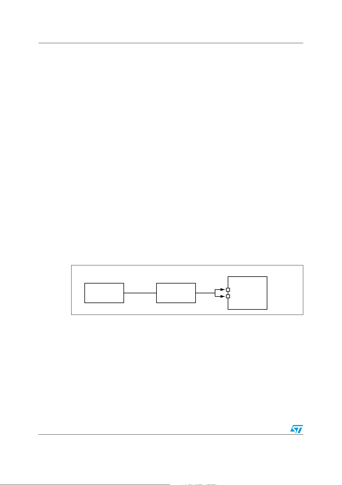
Ai17491
Sensor
Analog
voltage
Amplifier
(2)
Filter
(2)
ADC_CHx
(1)
COMP2_INP
(1)
STM32L1 device
1 Analog voltage monitoring
Ultra low power STM32L1 devices embed a 12-bit analog-to-digital converter (ADC) which
is very fast with a sampling rate of 1 Msample/s. However, with a 1.45 mA typical
consumption, it can jeopardize battery life time if left powered-on continuously. It is therefore
recommended to use analog comparators in application cases when analog input voltage
(sensor output) needs to be measured as soon as a pre-defined threshold is exceeded.
In STM32L1 devices, analog comparators are useful for monitoring the analog input voltage
and powering on the ADC when it is required. While monitoring the analog voltage, the
device can enter Stop mode at the same time that both comparators are still powered on.
Consequently, better consumption is achieved and power is saved.
Note: Analog comparators are powered by the internal reference voltage, V
powered on in Stop mode, and can be disabled by configuration. Once V
the comparators can no longer be used.
In an analog voltage monitoring application, where the sensor output voltage is lower than
the threshold, the MCU remains in Stop mode thereby saving power. As soon as the sensor
output exceeds the threshold, the MCU is woken up, the ADC is powered on, and the analog
input voltage is measured. When the sensor output is under the threshold, the MCU reenters Stop mode.
Average power consumption is dramatically reduced when compared with an application
that continuously measures the analog voltage whatever the input value.
Figure 1 shows how to connect a sensor output (temperature sensor, pressure sensor,
pyroelectric infrared detector, photodiode sensor) to an STM32L1 device in an analog
voltage monitoring application using comparator 2 (COMP2). COMP2 monitors the analog
voltage in Stop mode while the ADC measures it in Run mode.
Figure 1. Sensor output connection to COMP2
REFINT
REFINT
, which is still
is disabled,
1. Legend for Figure 1
ADC_CHx: AC channel x
COMP2_INP: comparator 2 non-inverting input
2. Only if required.
4/17 Doc ID 17758 Rev 3
Page 5
AN3248 Analog voltage monitoring
Ai18734
Sensor
Analog
voltage
Amplifier
(2)
Filter
(2)
COMP1_INP/
ADC_CHx
(1)
STM32L1 device
S R S R S
R S
Input analog voltage
Analog threshold
Time
MCU state
Time
Time
MCU current consumption
Few mA
Few μA
ai17492
Figure 2 shows how to connect a sensor output to an STM32L1 device using comparator 1
(COMP1). COMP1 shares the same inputs as the ADC which reduces the number of
required pins. Nevertheless, the threshold is fixed to V
REFINT
.
Figure 2. Sensor output connection to COMP1
1. Legend for Figure 2
COMP1_INP/ADC CHx: comparator 1 non-inverting input shared with ADC channel x
2. Only if required.
Figure 3 shows the gain in power consumption in an analog monitoring application.
Figure 3. Power consumption in an analog voltage monitoring application
1. Legend for Figure 3
S: Stop mode
R: Run mode
The input analog voltage can be connected either to PB4 or PB5. The analog threshold can
be provided internally through V
PB3. DAC channel 1 and channel 2 (DAC_OUT1 and DAC_OUT2 respectively) cannot be
used in such application cases since the DAC channels are powered off in Stop mode.
and its submultiples or via an external pin through
REFINT
Doc ID 17758 Rev 3 5/17
Page 6
Analog voltage monitoring AN3248
-
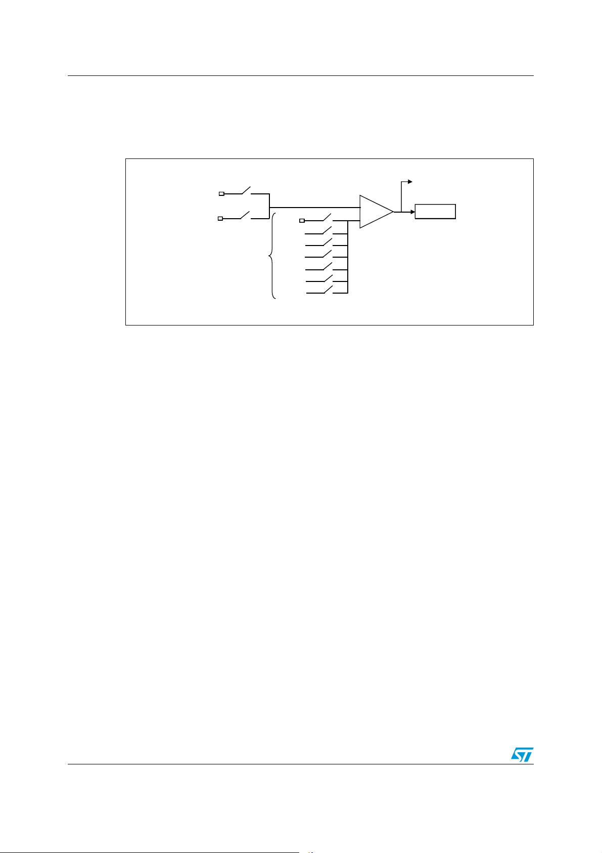
+
ai17493
GR6
GR6
PB4
PB5
Input voltage
COMP2
Wakeup
EXTI line 22
CMP2OUT
Analog threshold:
multiple sources
PB3
1/4 V
REFINT
1/2 V
REFINT
3/4 V
REFINT
V
REFINT
DAC_OUT2
DAC_OUT1
COMP2 wakes up the device from Stop mode through external interrupt line 22 (EXTI line
22).
Figure 4 shows the available configurations for inverting and non inverting inputs.
Figure 4. COMP2 configuration
1. Legend for Figure 4
DAC_OUT1: DAC channel 1 output
DAC_OUT2: DAC channel 2 output
V
: Internal reference voltage
REFINT
CMP2OUT: Comparator 2 output (internal output)
When the device enters Stop mode, only COMP2 and the internal reference voltage,
V
, remain powered on.
REFINT
Note: 1 Refer to the device datasheet for power consumption values.
2 In High-density devices, pins PB6 and PB7 can be used also as COMP2 non-inverting
inputs.
3 If the analog threshold corresponds to the internal reference voltage, V
REFINT
(1.22 V),
COMP1 can be used instead of COMP2 since it consumes much less power. In this case,
the input analog voltage can be connected to any channel among the 24 ADC channels.
6/17 Doc ID 17758 Rev 3
Page 7

AN3248 Analog watchdog during Stop mode
WNDE
PB5
Threshold2:
multiple sources
-
+
-
+
COMP1
COMP2
PB4
GR6
GR6
CMP1OUT
EXTI line 21
CMP2OUT
Wakeup
EXTI line 22
PB3
DAC_OUT1
DAC_OUT2
V
REFINT
3/4 V
REFINT
1/2 V
REFINT
1/4 V
REFINT
Input voltage
Wakeup
Threshold1:
V
REFINT
(1.22 V)
-1
-2
ai17494
2 Analog watchdog during Stop mode
The ADC in the STM32L1 family can be used as an analog watchdog with programmable
high and low thresholds. Nevertheless, the MCU must be kept in Run mode to be able to
watch analog voltage on input since the ADC is powered off in Stop mode. For ultra low
power STM32L1 devices, two analog comparators, COMP1 and COMP2, can be combined
in window mode and used as an analog watchdog that remains powered on while the MCU
is stopped. Consequently, lower consumption is achieved and power is saved.
Figure 5 displays the configuration of two such analog comparators in window mode.
Threshold1 is set to the internal reference voltage, V
among V
REFINT
, 3/4 V
REFINT
, 1/2 V
REFINT
, 3/4 V
REFINT
external pin PB3. The analog input voltage can be applied on group 6 of the analog switches
(PB4 or PB5).
Figure 5. Analog comparators combined in window mode
, and threshold2 is configurable
REFINT
, DAC_OUT1, DAC_OUT2, or the
Note: In High-density devices, pins PB6 and PB7 can be used also as COMP2 non-inverting
inputs.
DAC_OUT1 and DAC_OUT2 cannot be used in Stop mode since the DAC peripheral is
powered off.
Doc ID 17758 Rev 3 7/17
Page 8
Analog watchdog during Stop mode AN3248
In an analog watchdog application, COMP1 is configured through external interrupt line 21
(EXTI line 21) to exit the MCU from Stop mode when the analog input voltage exceeds
V
. COMP2 is set, through EXTI line 22, to exit the MCU from Stop mode when the
REFINT
analog voltage goes below the lower threshold. Throughout the time the analog voltage is
within the defined thresholds, the MCU is in Stop mode and power consumption is reduced.
When the analog voltage exceeds the defined thresholds, average power consumption can
be reduced by switching to Run mode.
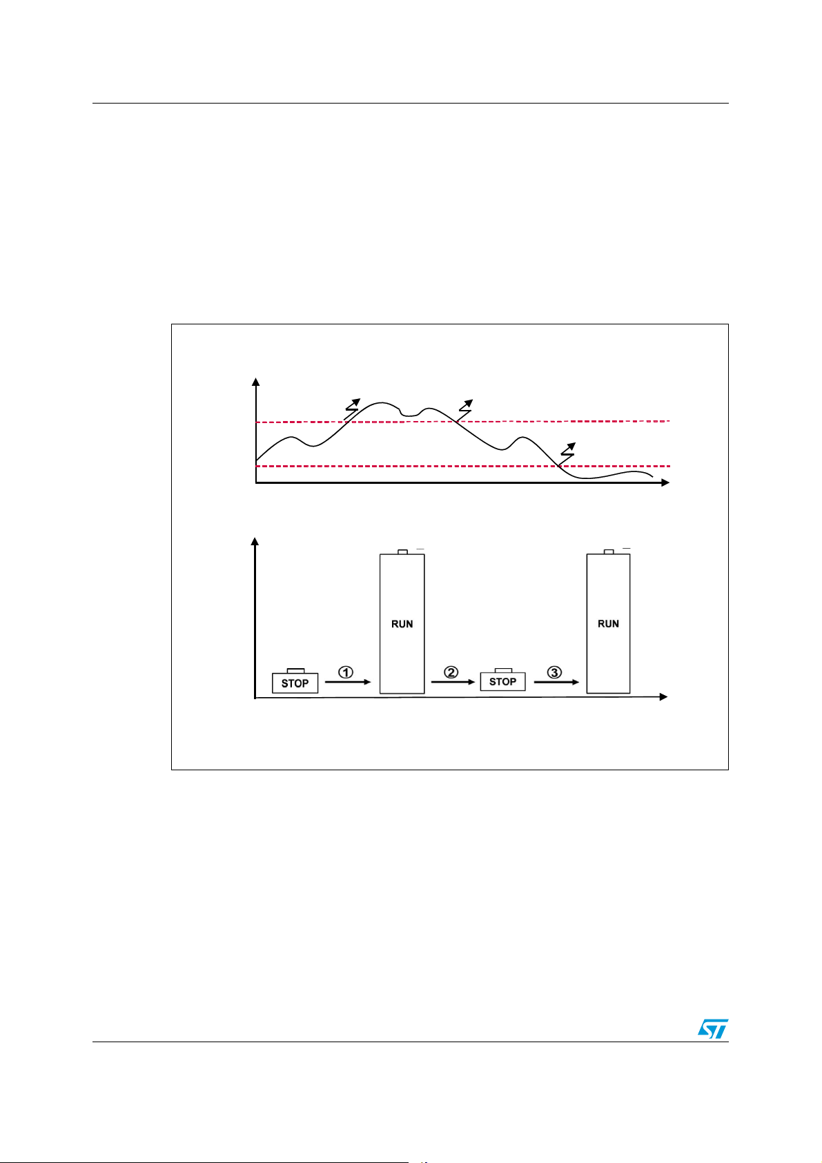
Figure 6 gives an overview of an analog watchdog application with threshold1 higher than
threshold2.
Figure 6. Analog watchdog during Stop mode
Sensor output
voltage
Threshold1:
V
REFINT
MCU exits
Stop mode
MCU enters
Stop mode
MCU exits
Stop mode
Threshold2
0 V
MCU state
1. While the MCU is in Stop mode, the input voltage exceeds threshold1 and the MCU exits Stop mode.
2. While the MCU is in Run mode, the input voltage goes below threshold1 and the MCU enters Stop mode.
3. While the MCU is in Stop mode, the input voltage goes below threshold2 and the MCU exits Stop mode.
Note: 1 In Stop mode, only COMP1, COMP2 and V
to the specific device datasheet for power consumption values.
2 No hysteresis is implemented on either comparator inputs.
continue to consume power. Please refer
REFINT
Time
Time
ai17495
8/17 Doc ID 17758 Rev 3
Page 9

AN3248 Pulse width measurement
PB5
-
+
COMP2
PB4
GR6
GR6
CMP2OUT
Wakeup
EXTI line 22
PB3
DAC_OUT1
DAC_OUT2
V
REFINT
3/4 V
REFINT
1/2 V
REFINT
1/4 V
REFINT
Input voltage
TIM2 IC4
TIM2 OCRECLR
TIM3 IC4
TIM3 OCREFCLR
TIM4 IC4
TIM4 OCRECLR
TIM10 IC1
OUTSEL[2:0]
ai18706
Threshold2:
multiple sources
-1
-2
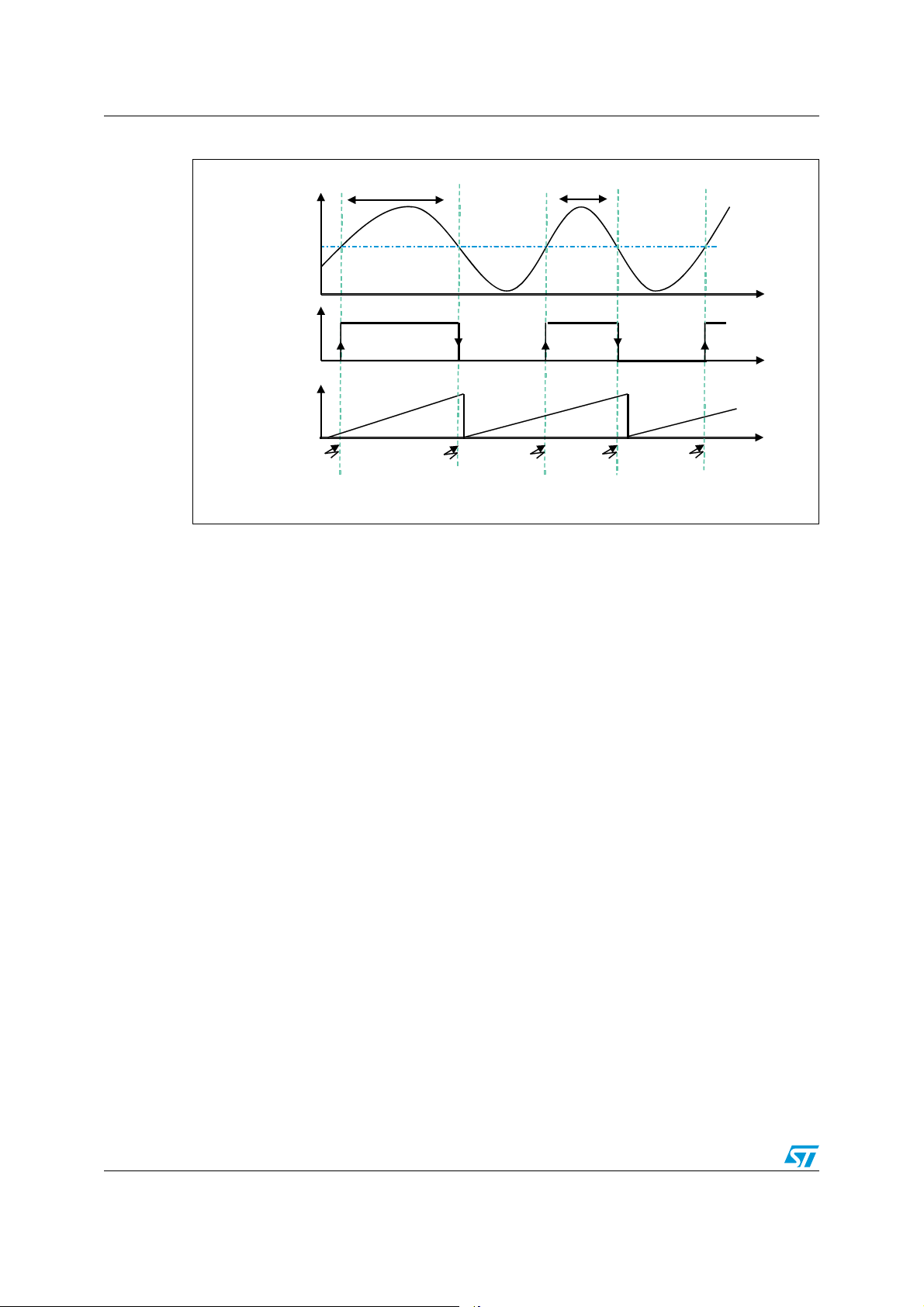
3 Pulse width measurement
In STM32L1 devices, the COMP2 output can be redirected to the input capture of the
embedded timers: TIM2, TIM3, TIM4, and TIM10. Redirecting the COMP2 output allows a
signal width or frequency with specific low and high levels (for example, a shifted signal) to
be measured. Figure 7 displays all the possible output redirections of the COMP2 output.
The input signal, whose signal width should be measured, is connected to any I/O of analog
switches group 6 (PB4 or PB5). The reference signal can be powered by:
● an internal reference (V
● the built-in DAC (channel 1 or channel 2)
● an external pin through PB3
The COMP2 output redirection is achieved through the OUTSEL[2:0] bits.
The timer input capture channel is configured to save the timer counter at both rising and
falling edges. When the input signal goes above the reference voltage, COMP2 output is at
a high level generating a rising edge on the timer input capture. When the input signal goes
under the reference voltage, COMP2 output is at low level generating a falling edge. The
elapsed time between the two consecutive events (falling then rising edge or rising then
falling edge) represents the pulse width. Hence, the pulse width measurement is performed
by simple subtraction of the counter values. Figure 8 gives an overview of the pulse width
measurement as measured by COMP2.
REFINT
, 3/4 V
REFINT
, 1/2 V
REFINT
, or 1/4 V
REFINT
)
Figure 7. COMP2 with output redirection feature
1. Legend for Figure 7
Note: In High-density devices, pins PB6 and PB7 can be used also as COMP2 non-inverting
DAC_OUT1: DAC channel 1 output
DAC_OUT2: DAC channel 2 output
V
: Internal reference voltage
REFINT
CMP2OUT: Comparator 2 output (internal output)
TIMx ICy: Timer x input capture channel y
TIMx OCREFCLR: Timer x output compare reference clear
inputs.
Doc ID 17758 Rev 3 9/17
Page 10
Pulse width measurement AN3248
Reference voltage
duration
(1)
1st capture
Low level
COMP2 output
high level
Input signal
Time
Time
Time
0
Timer counter
65535
duration
(1)
2nd capture
1st capture
2nd capture
1st capture
ai18707
Figure 8. Pulse width measurement: COMP2 output redirection to timer
1. The duration that should be measured
2. In the pulse width measurement application, COMP1 cannot be used since its output CMP1OUT (internal
output) is not connected to the embedded timers.
Note: 1 Signal frequency can be achieved by configuring the timer input capture channel to save the
counter value on only a rising or falling edge.
2 DAC outputs (DAC_OUT1 or DAC_OUT2) can be used as inverting inputs to allow the
reference voltage level (threshold) to be internally provided and programmable by software
from 0 V to V
DD
..
10/17 Doc ID 17758 Rev 3
Page 11

AN3248 PWM signal control
Time
PWM signal
Time
PWM signal at safe state (low level)
Time
COMP2 output is at high level
Low level
High level
COMP2 output
Current sensor output
Reference voltage
ai18708
4 PWM signal control
In STM32L1 devices, the COMP2 output can be redirected to the output compare reference
clear signal (OCREFCLR) of the embedded timers: TIM2, TIM3, and TIM4 (refer to Figure 7:
COMP2 with output redirection feature). The possibility of redirecting the COMP2 output can
be used to provide a fast response time that is independent from the system frequency
when an analog event occurs. This application case controls a PWM signal for motor control
when the current sensor output is connected to the COMP2 non-inverting input. In this
situation, the reference voltage is connected to the COMP2 inverting input. When the
current sensor output exceeds the selected threshold, the COMP2 output goes high and the
PWM signals switch to safe state.
Figure 9. PWM signal control: COMP2 output redirection to timer
Note: When the current sensor voltage reaches the reference voltage, the COMP2 output goes
1. In the pulse width measurement application, COMP1 cannot be used since its output CMP1OUT (internal
output) is not connected to the embedded timers.
high. Consequently, the PWM and output compare reference signals go low (to safe state).
Doc ID 17758 Rev 3 11/17
Page 12
Capacitance measurement AN3248
Input voltage VDD1tT⁄–()exp–()=
5 Capacitance measurement
The ability to connect the COMP2 output to the input capture channels of the timers allows
the capacitance value to be measured. The principle is based on measuring the charge time
of a resistor-capacitor (RC) network as follows:
● the charge time is measured
● the charge resistor (R) is already known
● the unknown capacitance (C) can be computed
Figure 10 shows the hardware connection of the RC network to an STM32L1 device.
Figure 10. RC network connection for capacitance measurement
STM32L1 device
TIMx OC
R
Input voltage
Threshold
C
COMP2
+
-
TIMx IC
ai18709
The capacitance measurement procedure consists of charging and discharging the
capacitor through the resistor. The charge/discharge function follows an exponential curve.
The charge function is given by Example 1.
Example 1
where:
● V
● t is the time
● T is the RC constant
is the positive supply voltage
DD
Charging and discharging the RC network is ensured by the timer output compare channel
(TIMx OC) configured in PWM mode. The timer channel is connected to the resistor.
The input voltage is connected to the COMP2 non-inverting input while the threshold is
connected to the COMP2 inverting input. When the input voltage crosses the threshold, the
COMP2 output switches to high level and a capture event occurs saving the counter value.
Figure 11 shows the capacitance measurement.
12/17 Doc ID 17758 Rev 3
Page 13
AN3248 Capacitance measurement
Threshold
TIMx OCy
Time
Input voltage
Time
Time
Capture event
0
Time
COMP2
output
65535
Timer counter
Capture event Capture event
ai18710
Threshold VDD 1 -tc T⁄()exp–()=
C t R 1-threshold VDD()⁄()ln×()⁄–=
CtK⁄–=
KR 1-thresholdVDD()⁄()ln×=
Figure 11. Capacitance measurement using COMP2
At the moment where the input voltage crosses the threshold and the COMP2 output
switches to high level, the charge function is given by Equation 1.
Equation 1
where “tc” is the time when the input voltage crosses the threshold
Using Equation 1 the capacitance value can be computed by Equation 2.
Equation 2
Usually R, the threshold, and V
are constant, so, measuring the capacitance is reduced
DD
to solving for Equation 3.
Equation 3
where K is solved using Equation 4
Equation 4
Doc ID 17758 Rev 3 13/17
Page 14

Brightness control using a light dependent resistor (LDR) AN3248
V
DD
COMP2
Resistor (R)
V
IN
Other possibilities
V
REFINT
PB3
¾ V
REFINT
½ V
REFINT
¼ V
REFINT
PB4/PB5
(1)
+
-
EXTI line 22
ai18728
CMP2OUT
Light dependent
resistor (LDR)
STM32L1 device
V
IN
LDR
LDR R+()
--------------------------- -
V
DD
×=
6 Brightness control using a light dependent resistor
(LDR)
In some battery operated applications, the microcontroller needs to be powered if the
environment is lit; otherwise, it must be kept powered-off. For such applications, a light
dependent resistor (LDR), whose resistance depends on light intensity, is useful to control
the microcontroller state. Using an LDR sensor, the microcontroller can switch to/from Lowpower mode depending on the voltage provided by the LDR resistor. Figure 12 shows how
to connect an LDR resistor to an STM32L1 device. COMP2 non-inverting input can be
connected to an LDR resistor through a voltage divider (V
externally to PB3 or set internally to V
REFINT
, 3/4 V
REFINT
COMP2 output (CMP2OUT) can be internally connected to EXTI line 22 which, when
configured to detect both rising and falling edges on CMP2OUT, can be used as an interrupt
source to switch to/from Low power mode.
Figure 12. Connecting an LDR resistor to an STM32L1 device
). The threshold can be set
IN
, 1/2 V
REFINT
, or 1/4 V
REFINT
. The
1. PB4 or PB5 can be used as COMP2 non-inverting input. Thus, VIN can be connected to PB4 or PB5.
The voltage VIN can be computed using Equation 5.
Equation 5
As the LDR resistance decreases with increasing light intensity, the voltage V
as more light shines on the LDR.
14/17 Doc ID 17758 Rev 3
decreases
IN
Page 15

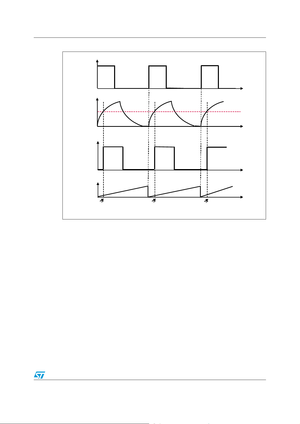
AN3248 Brightness control using a light dependent resistor (LDR)
Threshold
Time
Time
Low level
High level
Dark LightLight
VIN > threshold VIN < threshold
V
IN
Microcontroller enters
Low power mode
Microcontroller exits
Low power mode
CMP2OUT
EXTI22
ai18729
The top part of Figure 13 shows the evolution of VIN as a function of light variation. The
selected threshold (COMP2 inverting input) defines the limit of dark/light. The bottom part of
Figure 13 shows that COMP2 output (CMP2OUT) level depends on V
and consequently
IN
on light intensity. Using EXTI line 22 (which is internally connected to CMP2OUT), the
microcontroller can detect the CMP2OUT level switch (from a high level to a low level or vice
versa).
Figure 13. Comparator output behavior versus light intensity
The LDR resistor can be used in other microcontroller-based applications rather than
darkness control (for example: DC relay control and AutoFocus).
For other uses of analog comparators using LDR resistors, refer to the STM32L152-EVAL
(for STM32L1xx Ultra Low Power Medium-density devices) or to STM32L152D-EVAL (for
STM32L1xx Ultra Low Power High-density devices) demonstration firmware. In this
demonstration, the LCD glass contrast is adjusted according to the luminosity detected
using the LDR resistor.
Doc ID 17758 Rev 3 15/17
Page 16

Revision history AN3248
7 Revision history
Table 1. Document revision history
Date Revision Changes
10-Jan-2011 1 Initial release.
12-Jan-2012 2
07-Feb-2012 3
Document updated to include Ultra Low Power High-density device
features.
Updated notes under Figure 4: COMP2 configuration, Figure 5:
Analog comparators combined in window mode and Figure 7:
COMP2 with output redirection feature.
16/17 Doc ID 17758 Rev 3
Page 17

AN3248
Please Read Carefully:
Information in this document is provided solely in connection with ST products. STMicroelectronics NV and its subsidiaries (“ST”) reserve the
right to make changes, corrections, modifications or improvements, to this document, and the products and services described herein at any
time, without notice.
All ST products are sold pursuant to ST’s terms and conditions of sale.
Purchasers are solely responsible for the choice, selection and use of the ST products and services described herein, and ST assumes no
liability whatsoever relating to the choice, selection or use of the ST products and services described herein.
No license, express or implied, by estoppel or otherwise, to any intellectual property rights is granted under this document. If any part of this
document refers to any third party products or services it shall not be deemed a license grant by ST for the use of such third party products
or services, or any intellectual property contained therein or considered as a warranty covering the use in any manner whatsoever of such
third party products or services or any intellectual property contained therein.
UNLESS OTHERWISE SET FORTH IN ST’S TERMS AND CONDITIONS OF SALE ST DISCLAIMS ANY EXPRESS OR IMPLIED
WARRANTY WITH RESPECT TO THE USE AND/OR SALE OF ST PRODUCTS INCLUDING WITHOUT LIMITATION IMPLIED
WARRANTIES OF MERCHANTABILITY, FITNESS FOR A PARTICULAR PURPOSE (AND THEIR EQUIVALENTS UNDER THE LAWS
OF ANY JURISDICTION), OR INFRINGEMENT OF ANY PATENT, COPYRIGHT OR OTHER INTELLECTUAL PROPERTY RIGHT.
UNLESS EXPRESSLY APPROVED IN WRITING BY TWO AUTHORIZED ST REPRESENTATIVES, ST PRODUCTS ARE NOT
RECOMMENDED, AUTHORIZED OR WARRANTED FOR USE IN MILITARY, AIR CRAFT, SPACE, LIFE SAVING, OR LIFE SUSTAINING
APPLICATIONS, NOR IN PRODUCTS OR SYSTEMS WHERE FAILURE OR MALFUNCTION MAY RESULT IN PERSONAL INJURY,
DEATH, OR SEVERE PROPERTY OR ENVIRONMENTAL DAMAGE. ST PRODUCTS WHICH ARE NOT SPECIFIED AS "AUTOMOTIVE
GRADE" MAY ONLY BE USED IN AUTOMOTIVE APPLICATIONS AT USER’S OWN RISK.
Resale of ST products with provisions different from the statements and/or technical features set forth in this document shall immediately void
any warranty granted by ST for the ST product or service described herein and shall not create or extend in any manner whatsoever, any
liability of ST.
ST and the ST logo are trademarks or registered trademarks of ST in various countries.
Information in this document supersedes and replaces all information previously supplied.
The ST logo is a registered trademark of STMicroelectronics. All other names are the property of their respective owners.
© 2012 STMicroelectronics - All rights reserved
STMicroelectronics group of companies
Australia - Belgium - Brazil - Canada - China - Czech Republic - Finland - France - Germany - Hong Kong - India - Israel - Italy - Japan -
Malaysia - Malta - Morocco - Philippines - Singapore - Spain - Sweden - Switzerland - United Kingdom - United States of America
www.st.com
Doc ID 17758 Rev 3 17/17
 Loading...